
 Open Access Article
 This Open Access Article is licensed under a Creative Commons Attribution-Non Commercial 3.0 Unported Licence
Ordered growth of metal oxides in patterned multi-angle microstructures†
Zhenkai Jiabc,
Min Sun a,
Tiantian Chena,
Xinyi Shena,
Xiuzhen Xua,
Yan Zhongd,
Dadong Wangd,
Jiwei Maa,
Bo Chen*a,
Zhiguo Yibc and
Xiaobin Xu*a
a,
Tiantian Chena,
Xinyi Shena,
Xiuzhen Xua,
Yan Zhongd,
Dadong Wangd,
Jiwei Maa,
Bo Chen*a,
Zhiguo Yibc and
Xiaobin Xu*a
aKey Laboratory of Advanced Civil Engineering Materials of Ministry of Education, Shanghai. Key Lab. of D&A for Metal-Functional Materials, School of Materials Science & Engineering, Institute for Advanced Study, Tongji University, Shanghai 201804, China. E-mail: xiaobinxu@tongji.edu.cn; bo.chen@tongji.edu.cn
bState Key Laboratory of High-Performance Ceramics and Superfine Microstructure, Shanghai Institute of Ceramics, Chinese Academy of Sciences, Shanghai 200050, China
cUniversity of Chinese Academy of Sciences, Beijing 100049, China
dShanghai Highway Investment Construction and Development Co., Ltd., Shanghai 200336, China
First published on 1st June 2023
Abstract
Herein, we report a facile method combining top-down patterning transfer and bottom-up nanorod growth for preparing large-area and ordered TiO2 nanorod arrays. Pre-crystallization seeding was patterned with nanostructured morphologies via interfacial tension-driven precursor solution scattering on various types and period templates. This is a widely applicable strategy for capillary force-driven interfacial patterns, which also shows great operability in complex substrate morphologies with multiple-angle mixing. Moreover, the customized patterned lithographic templates containing English words, Arabic numerals, and Chinese characters are used to verify the applicability and controllability of this hybrid method. In general, our work provides a versatile strategy for the low-cost and facile preparation of hydrothermally growable metal oxide (e.g., ZnO and MnO2) nanostructures with potential applications in the fields of microelectronic devices, photoelectric devices, energy storage, and photocatalysis.
1. Introduction
Micro & nano technology (MNT) refers to the design, processing, system integration and application technology of components with micron, sub-micron, and nanometer scales in its constituent systems, which also involve multidisciplinary and multi-disciplinary intersections.1 It is generally accepted that micron-scale processing refers to the fabrication of tiny structures of 0.1–100 μm in size, while 0.1–1 μm is commonly referred to as the submicron range. Nanoscale processing refers to the process of producing tiny structures of 1–100 nm in size. In the past decades, MNT has been rapidly developed to the nano-level for fine regulation of material properties. In detail, the facile and unconstrained patterning processes are necessary when it comes to device applications, such as microelectronic devices2,3 and semiconductor components.4 Among them, additive or subtractive manufacturing-based fabrication techniques such as mechanical micromachining,5 laser direct writing,6 photolithography,7 epitaxial growth,8 and transfer printing9 play an important role in device integration. In particular, photolithography is a simple and low-cost method for large-scale preparation and plays a key role in the field of MNT processing.Titanium dioxide (TiO2) is a typical n-type semiconductor material with a band gap of 3.0–3.2 eV.10 It is an abundant, non-toxic and chemically stable material with excellent optoelectronic properties and outstanding semiconductor properties. A variety of TiO2 nanostructures, including nanoparticles,11 nanorods,12,13 nanowires,14 nanotubes,15 and nanosheets,16 play a great role in photocatalysis,17 solar cells,18 ion batteries,19 supercapacitors,20 photochemical sensors,21,22 biomedical applications,23 and other applications. The traditional methods for fabricating TiO2 nanostructures include electrochemical deposition,24 chemical vapor deposition,25 template method,26 hydrothermal treatment,27 and sol–gel method.28 The hydrothermal method is a simple, economical, and high-yield bottom-up method for growing single-crystal TiO2 nanorods. The TiO2 nanorod grown by hydrothermal epitaxial are characterized by high crystallinity, controllable size and uniform morphology, but the TiO2 nanorod fabricated by this method have certain limitations, i.e., the grain size distribution, major crystalline phase orientation and surface growth sites are rather random. This makes it impossible for traditional hydrothermal methods to fabricate ordered patterned TiO2 nanostructures for more complex applications, such as nano-components,29 microelectronic devices and integrated fabrication.30,31
As a traditional top-down patterning method for different materials, lithography is widely used in the semiconductor industry. When directly applied to rigid materials, such approaches usually have the disadvantage of high cost, as they either require expensive equipment or have low flux.32 Therefore, they are not suitable for the scalable patterning applications of metal oxide crystals. One strategy to address this challenge is to develop a hybrid method,33–35 i.e., a combination of a top-down pattern transfer method and a bottom-up nanomaterial growth method,36–39 that is capable of forming arbitrary patterns. J. Volk's group40 successfully prepared vertically aligned hexagonal ZnO nanorod arrays by using polystyrene nanospheres as a mask for lithography. Rusen Yang's group41 developed a vertical ZnO nanowire array grown on a flexible polyethylene terephthalate substrate based on a hydrothermal method, which was applied to strain sensors with high stability and fast response time.
In this work, we report a hybrid approach combining top-down and bottom-up processes to prepare patterned arrays of large-area and ordered TiO2 nanostructures by directionally dispersing the spin-coated precursor on the template surface, and hydrothermal growth treatment of the shaped nucleated crystalline seed layer. The seed layer molding can be applied in a variety of micro/nano structure templates, such as linear, mesh, and inverted pyramid, as well as a wide range of angle types, including acute, right angle, and obtuse angle. In addition, the effects of the growth temperature, duration and reaction concentration on the structural morphology of the TiO2 nanorods are investigated, and the controlled growth of the TiO2 nanorod in terms of the crystal morphology, structural sparsity and cluster orientation are achieved at pre-designed positions. This work makes three-dimensional patterned nanomaterial arrays more convenient and accessible, i.e., homogeneous and ordered metal oxide (e.g., ZnO and MnO2) nanostructure arrays with potential applications in the fields of optoelectronics,42,43 energy storage,44 catalysis,45–47 and biomedicine.48–51
2. Experimental section/method
2.1. Materials
The self-designed hard mask was customized from Xi'an Boyan Micro-Nano International Technology Co., Ltd. (China); the silicon oxide wafers (P100) of ∼700 μm were purchased from Suzhou Crystal Silicon Electronics & Technology Co., Ltd. (China); the positive photoresist HTI-751, negative photoresist SUN-9i and ZX-238 developer were acquired from Suzhou Research Materials Microtech Co., Ltd. (China); the specialty gases of the preparation process were from Shanghai Xiangkun Special Gas Co., Ltd.; anhydrous potassium hydroxide (KOH) was purchased from Shanghai Aladdin Biochemical Technology, Co., Ltd. (China); all of the chemicals without special declaration were obtained from Sinopharm Group Corp. (China).2.2. Fabrication devices
The P15 O2-gas plasma dry cleaner and 280 reactive ion etching (RIE) machine were purchased from Hefei Poly Vacuum Science and Technology, Ltd. (China); The 12A spin-processor was from Zhangqiu Guanpai Electronic Equipment Factory (China); the SX2 electric box resistance furnace was obtained from Shaoxing Shangyu Daoxu Kexi Instrument Factory (China); the DHG-9 benchtop electric constant temperature blast oven was customized from Shanghai Yiheng Technology Instrument Co., Ltd. (China); the hydrothermal reactor was from Xi'an Yibeier Instrument Equipment Co., Ltd. (China). The WH220 heated magnetic agitator was from Wiggens Technology (Beijing) Co., Ltd.2.3. The fabrication of SiO2 templates with nanostructure arrays
Before the fabrication of the nanostructure templates, the cut-out SiO2/Si (P100) (SiO2 at ∼100 nm thickness, Si at ∼600 nm thickness) wafer processed in a Teflon flower basket with the piranha solution or organic solvents was ultrasonically treated for 60 min. After blow-drying with the gas gun, the wafer was processed in an O2 plasma device (cavity pressure: 10–20 Pa, work power: 100–150 W, and work time: 120–180 s). The photoresist was coated through a spin-processor to form a uniform film on the surface of the silicon oxide substrate (spin-coat conditions: 2000 rpm for 40 s). Then, using the ultraviolet lithography machine to expose, the pattern was transformed from the hard mask to photoresist. After development, the periodic nano-pattern arrays of the SiO2 substrate were presented, and a post-bake process was used to increase the etching resistance of the photoresist. The periodic nano-pattern of the photoresist film was transferred to the SiO2 layer through the dry etching treatment (gas composition: CHF3![[thin space (1/6-em)]](https://www.rsc.org/images/entities/char_2009.gif) :CF4 = 1:1 in volume, cavity pressure: 15 Pa, work power: 300 W, etching time: 10 min). The residual photoresist was taken down from the substrate via the removal immersion. With the protection of the surface SiO2, the pre-design morphology of the Si wafer was formed under KOH-anisotropic etching. The deionized water was employed for removing the residual alkali of the surface substrate, and the remaining SiO2 layer was dissolved in diluted HF solution (5–10% aq.) for immersion for 10 min. A ∼100 nm thick SiO2 film was uniformly thermally grown on the silicon nano-pattern substrate via a period of calcination in a muffle furnace.
:CF4 = 1:1 in volume, cavity pressure: 15 Pa, work power: 300 W, etching time: 10 min). The residual photoresist was taken down from the substrate via the removal immersion. With the protection of the surface SiO2, the pre-design morphology of the Si wafer was formed under KOH-anisotropic etching. The deionized water was employed for removing the residual alkali of the surface substrate, and the remaining SiO2 layer was dissolved in diluted HF solution (5–10% aq.) for immersion for 10 min. A ∼100 nm thick SiO2 film was uniformly thermally grown on the silicon nano-pattern substrate via a period of calcination in a muffle furnace.
2.4. TiO2 seeding precursors
A certain amount of TiO2 seed precursor was prepared. A total volume of 1.0 mL concentrated HCl (AR, ∼30% aq., Sigma Aldrich) was mixed with 25.0 mL of isopropanol (AR 99%, Sigma Aldrich) for rotating at 1000 rpm for 30 min in room temperature. Varied amounts of tetra-n-butyl titanate (C16H36O4Ti, 99%, Sigma Aldrich) were added slowly to the mixture under rotation. The solution was then stored in the reagent refrigerator for later use.2.5. TiO2 growth precursors
The TiO2 nanorod precursor solution was fabricated using similar methods. A volume of 120 mL hydrochloric acid (30% aq.) and 120 mL isopropanol were mixed and rotated at 1000 rpm for 30 min. An amount of tetra-n-butyl titanate was added slowly to the mixture using a pipette gun (4 M: add 4 mL tetra-n-butyl titanate). The solution was stored in the reagent refrigerator for later use.2.6. Capillary force assisted nucleation of TiO2 on the nanostructure arrays
In order to realize the capillary force-assisted TiO2 seeding precursors controlled nucleation, a homogeneous spin-coating strategy was adopted to disperse the dilute mixture solution. The silicon oxide substrate with nanostructure array was treated by plasma cleaner (gas: high-purity O2, cavity pressure: 15–20 Pa, work power: 100 W, and treatment time: 180 s) to increase the surface hydrophilicity. A volume of 200 μL of the seeds precursor solution was dropped onto the SiO2 template, and then a spin-coating process (3500 rpm for 40 s) was performed to remove excess solvent. The SiO2 templates were heated on a plate heater at 150 °C under normal atmosphere for 5 min. In the process of heating and concentration, the seed precursor solution gradually formed the solid–liquid mixed phase of precrystallization. The mixture with mobility wets the micro–nano structure template, and is uniformly distributed at the corresponding angles by means of capillary forces. For crystallizing the TiO2 seeds nucleation in the pre-selected area and enhancing the interfacial bonding force, the SiO2 template with nanostructure arrays covered with TiO2 seeds was calcined in a muffle furnace at 600 °C for 120 min.2.7. Pattern growth of the TiO2 nanorod arrays
Firstly, the SiO2 nanostructure arrays template coated with TiO2 seed should be prepared by spin-coat process and calcination treatment according to experimental requirements. Then, ∼20 mL as-prepared TiO2 growth precursor solution was transferred into a 50 mL Teflon high-temperature reactor, in which the reaction template base had been pre-placed. The high-temperature reactors were placed in the pre-heated electric oven at 140–200 °C for a certain amount of time. After the reaction was cooled to room temperature, the products were separated carefully from the Teflon container. The substrate was washed with deionized water and absolute ethanol three times, then heated at 450 °C for 1 h to remove the surface organic attachment. When the muffle furnace was cooled, the pattern-grown TiO2 nanorod arrays were prepared for subsequent characterization.2.8. Materials characterizations
Scanning electron microscopy (SEM) images of the microscale morphology were obtained on a Zeiss Sigma 300 VP operated at 0–20 kV. At room temperature, the X-ray diffraction (XRD) data were collected through a Bruker D8 Advance powder diffractometer (operating at 40 kV, 40 mA, a Cu-Kα source) fitted with a beryllium window.3. Results and discussions
3.1. Preparation of TiO2 nanorod arrays on patterned substrates
The patterned TiO2 nanorod arrays were fabricated by the combined top-down and bottom-up approaches, the major tenets of which are shown in Scheme 1. The pre-designed templates were obtained by traditional top-down processes, e.g., ultra-violet (UV) lithography, RIE process, and wet etching techniques. The patterned TiO2 nanorod arrays were then fabricated on the prepared templates by the bottom-up process, including solution crystallization precipitation and in situ thermal growth.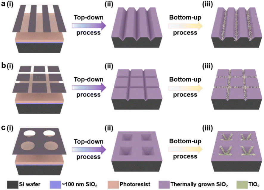 | ||
| Scheme 1 The fabrication scheme of the TiO2 nanorod arrays via top-down (photolithography) and bottom-up (hydrothermal growth) methods in various templates. The linear template is prepared via photolithography by transferring the pattern from a hard mask to silicon substrate; the region-selective linear TiO2 nanorod arrays are generated by thermal growth of coated seeds. (a) The linear template. (b) The mesh template. (c) The pyramidal template. | ||
The lithography hardmask was designed based on the preliminary results that had been explored, and the processing and preparation were entrusted to the qualified related enterprises. A cleaning surface facilitates the formation of uniform and stable photoresist films during the lithography process. Thus, the cleaning process is a necessary precondition for the promising UV-lithography process in SiO2–Si wafers. During this process, the combination of piranha solution, organic cleaning solvents, ultrasonic washing, and oxygen-plasma cleaning is used. In Fig. 1, a layer of photoresist is spin-coated onto a clean SiO2–Si wafer, and the photoresist is dried on a heated plate at 90 °C for 60 s. UV exposure is then performed with a photolithograph to produce a photoresist film containing the transfer pattern. The unprotected SiO2 was eliminated via the dry etching process. Thus, the periodic pattern is further transferred to the SiO2 layer. Regular arrays of nanostructures are produced on the Si substrate by anisotropic wet-etching under the protection of the SiO2 hard-mask. After removing the surface alkaline and residual SiO2, the substrates are calcined in a muffle furnace for oxidizing in an external-to-internal manner. Finally, a SiO2 template capable of growing a nanorod is formed. As shown in Fig. 1a(v)–c(v), the linear template, the pyramidal template and the mesh template are fabricated using similar approaches. These included angles generated by the substrate microstructure are quite different, such as ∼70° for V-shaped nanowires, ∼110° for inverted nanopyramids, and ∼90° for network structures. This angle is designed based on the intrinsic crystalline phase and nanostructure morphology of the silicon wafers, which is influenced by macroscopic wet-etching conditions, etchant type, reaction temperature, etching solution concentration, and others. Although there were inevitable errors between the actual preparation process and the ideal templates, a series of templates with different styles of angle were still prepared with sufficient experience, including acute angle, right angle, and obtuse angle.
 | ||
| Fig. 1 The detailed schematic for developing the different substrate templates using the traditional top-down approaches. (a) The linear template. (b) The mesh template. (c) The pyramidal template. (i) Photolithography is used to transfer the pattern from the hard mask to the photoresist on the silicon substrate through ultraviolet light. (ii) After developing, the patterned photoresist is formed on the silicon wafer. (iii) Under the protection of the patterned photoresist, the dry-etching machine is used to corrode the exposed SiO2 film. (iv) After a period of reaction in a hot alkaline solution, anisotropic etching occurs on the exposed surface of the silicon wafer to produce the target morphology. (v) The substrate is cleaned and calcined in a muffle furnace, and then the SiO2–Si template is formed. | ||
3.2. The growth regulation of TiO2 nanorod arrays
As illustrated in Fig. 2a, the bottom-up nanorod growth strategy consists of two components: crystal seed forming and nanorod in situ growth. Both are critical for the microscopic morphology of the SiO2–Si template. For this multi-influence factors problem, the orthogonal decomposition and univariate control method is used. Firstly, the linear template was selected for an intensive study of crystal seed formation because of its relatively simple morphology. After the pre-spin coating, a finite precursor solution is formed in the surface microstructure of the linear template. The volume of the solution decreases gradually during the process of heating and concentration, and the precipitated crystals are evenly distributed in the bottom of the V-shaped groove under the action of capillary force, and a patterned crystalline seed layer is formed in Fig. 2a(ii). The SEM images of the crystalline morphology, corresponding to different precursor solution concentrations, are presented in Fig. 2b. With the increase of TiO2 precursor content in the mixture, the effective volume of nucleated seeds in the patterned nanoarray increased. It can be found from the SEM images that the volume occupied by the seeds in the V-groove increases, the bottom surface of the inverted trapezoidal slot increases, and the depth decreases. Even though these three kinds of seed layers are reacted under the same thermal growth conditions, significant differences in nanorod morphology are shown. In practical application, it is observed that the seed layer formed by 0.001 M concentration precursor is smaller in size with a smaller contact area with the substrate after nucleation and a weaker bonding strength. Especially under high temperature and pressure conditions, the seed layer separation is easily separated from the substrate. The nanorod might fall off or grow chaotically in some regions, destroying the whole homogeneity and regioselective of the TiO2 nanorod. The seed layer formed by the 0.01 M concentration precursor has a larger contact area with the substrate and stronger bonding strength after nucleation. However, the seed precipitation formed during high-temperature calcination is not the major crystalline phase of the hydrothermally grown nanorod, and the excessive seed layer will reduce the crystallinity of the nanorod in the template. A related phenomenon has been reported in fundamental studies.52,53 As shown in the linear template of Fig. S1(i),† the initial nanorod growth location is the edge of the crystallized seed layer. More obvious contrast results are observed in the inverted pyramidal template in Fig. S1(ii).† Therefore, the ∼0.003 M concentration solution precipitates crystals with less differential impact to form the seed layer during the drying process, which makes it a great choice to continue the morphological investigation. | ||
| Fig. 2 (a) The detailed scheme is shown employing the conventional bottom-up approach for TiO2 nanorod growth in substrate templates. (i) The pre-fabricated TiO2 seed solution is spin-coated on the SiO2–Si template. (ii) The dispersed solution precipitates crystals in the drying process, and forms a seed layer. (iii) The linear TiO2 nanorod arrays were hydrothermally growing on the crystalline seed. (b) SEM images of the morphological changes of the TiO2 crystalline seeds after drying treatment at different precursor concentrations. Scale bars: 5 μm. | ||
The TiO2 hydrothermal process occurring in the precursor solution can be described by the hydrolysis reaction of tetrabutyl titanate and the condensation reaction of the titanium intermediates.54 The TiO2 nanostructure morphology of conventional hydrothermal treatment involves a variety of factors, including growth period, heating temperature, and reaction concentration.55,56 We have investigated the effects of these conditions on the morphological evolution of TiO2 growth processes through a single control variable approach to obtain TiO2 nanorod arrays with controllable morphology, easy preparation, and high reproducibility. In Fig. 3a, the typical SEM images of the TiO2 nanorod array are obtained on the linear template at different reaction times from 0.5 h to 3 h. The average size of the nanorod obtained at different times is measured and summarized in Fig. 4a. With increasing reaction time, the lengths and diameters of the nanorod increase from unmeasurably small sizes to ∼0.743 μm and ∼0.162 μm, respectively. The results show that the beginning stage of the hydrothermal reaction is dominated by TiO2 nanocrystal formation, and the size of the nanorods increases over a long period of time. The dependence of the morphological evolution of the TiO2 nanorod on the reaction temperature is shown in Fig. 3b and 4b. As the reaction temperature increases, the length and diameter of the nanorod increase from ∼0.381 μm and ∼0.048 μm to ∼0.985 μm and ∼0.244 μm, respectively. A small number of micro-sized TiO2 nanorods are formed under a low growth temperature of 140 °C, indicating that a reaction temperature higher than 140 °C is required to obtain large-scale TiO2 nanorods with limited reaction time. At the same time, if the reaction temperature is too high, the substrate surface morphology will be ignored with limited reaction time (2 h), i.e., the TiO2 nanorod will spread over the whole substrate and even fill the surface gap of the substrate microstructure to form a plane TiO2 film (Fig. 3b). According to the SEM data in Fig. 3c and the statistical result in Fig. 4c, it is obvious that the rapid growth mutation of the TiO2 nanorods slows down after the mass concentration of the growth precursors exceeds 8 M, and the size is maintained at ∼2 μm length and ∼0.5 μm diameter. We have characterized the typical crystal structures prepared by XRD analysis. The XRD results in Fig. 4d demonstrate that the as-prepared TiO2 is the rutile phase,57 i.e., the characteristic peaks in the XRD spectra can be attributed to the TiO2 (110), (101), (111), (211) and (220) crystal planes. In summary, TiO2 nanorod arrays with ideal size, reasonable density, and directional distribution can be easily obtained by simply adjusting the hydrothermal temperature, growth time, and reaction precursor concentration.
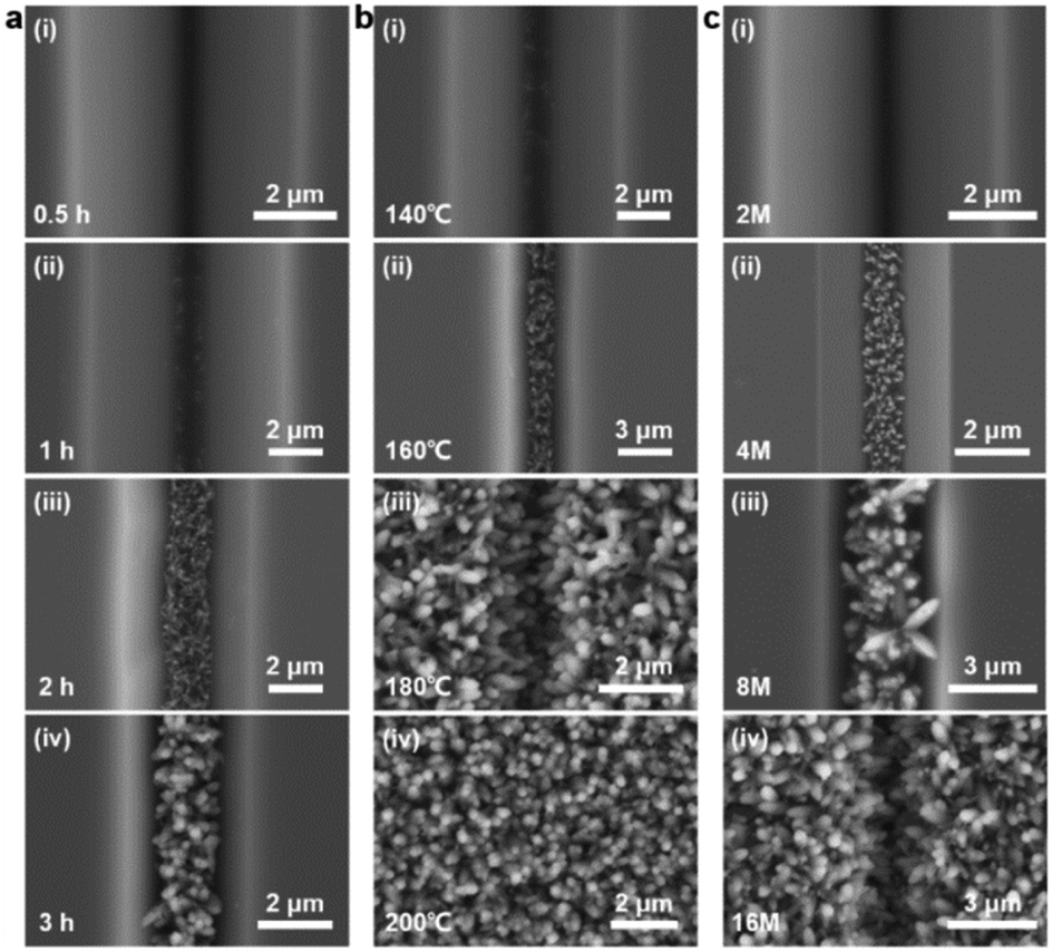 | ||
| Fig. 3 (a) SEM images of the TiO2 nanorod arrays grown at different reaction times: (i) 0.5 h, (ii) 1 h, (iii) 2 h, and (iv) 3 h (temperature: 170 °C, concentration: 4 M). (b) SEM images of the temperature-dependent growth of TiO2 nanorod arrays. (i) 140 °C, (ii) 160 °C, (iii) 180 °C, and (iv) 200 °C (time: 2 h, concentration: 4 M). (c) SEM images of the TiO2 nanorod arrays according to different reactant concentrations. (i) 2 M, (ii) 4 M, (iii) 8 M, and (iv) 16 M (time: 2 h, temperature: 170 °C). | ||
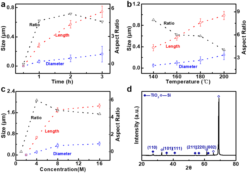 | ||
| Fig. 4 (a–c) Statistical schematic of the average diameters, lengths and aspect ratio of the TiO2 nanorod under different reaction conditions: (a) time, (b) temperature, (c) concentration. (d) The XRD data of the TiO2 nanorod arrays on the linear template substrate (template is ∼5 μm groove and 10 μm arrays period. Scale bar marked in the figure). | ||
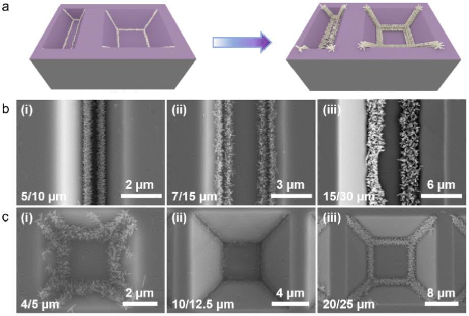
Based on the experimental results of the morphology control of the TiO2 nanorods in pre-prepared templates, we have applied them in different sizes of linear templates, and found that they showed excellent applicability and stability. Fig. 5a shows the SEM images of the TiO2 nanorods employed in the linear templates ranging from a few micrometers to dozens of micrometers. When the microstructure is formed at a sharp angle, the capillary force can play a full role in template with different sizes, resulting in directional and continuous nucleation of the precursor to create a crystal seed layer. The seed site for the subsequent thermal growth can be employed to form a tunably controlled, continuous and homogeneous array of TiO2 nanorods. If the linear template is treated as a one-dimensional (1D) template, we expand the template dimension to form a planar two-dimensional (2D) mesh template and a three-dimensional (3D) inverted pyramid template, and attempt to introduce the nanorod growth mechanism into them. As shown in Fig. 5b and c, similar results are also exhibited with other types of templates. The seed layer is patterned with the same method; that is, after spinning the coating solution and heating crystallization, the precursor of the solid–liquid mixture phase is evenly distributed along the microstructure angle under the action of capillary force. The SEM images show that in both 2D and 3D templates, the precursor solution crystallizes and nucleates at pre-designed locations, and the TiO2 nanorod in turn grows directionally along the seed layer distribution to form a patterned nanorod array cluster. Similarly, in substrates with different periods, the 2D and 3D templates also exhibit solution capillary force drive effects, i.e., spin-coated precrystallization can still be applied in nanostructures with right angles or obtuse angles, which significantly enhances the potential application of the method.
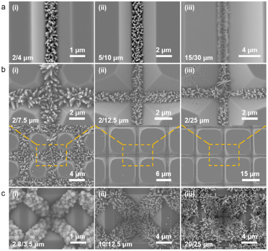 | ||
| Fig. 5 (a) SEM images of the TiO2 nanorod arrays in linear templates with different periods: (i) ∼2 μm V-shaped groove, 4 μm template cycle. (ii) ∼5 μm V-shaped groove, 10 μm template cycle. (iii) ∼15 μm V-shaped groove, 30 μm template cycle. (b) SEM images of the TiO2 nanorod arrays in mesh templates with different periods: (i) ∼2 μm mesh lines, 7.5 μm template cycle. (ii) ∼2 μm mesh lines, 12.5 μm template cycle. (iii) ∼2 μm mesh lines, 25 μm template cycle (detail enlargement at the top). (c) SEM images of the TiO2 nanorod arrays in pyramidal templates with different periods: (i) ∼2.8 μm inverted pyramid, 3.5 μm template cycle. (ii) ∼10 μm inverted pyramid, 12.5 μm template cycle. (iii) ∼20 μm inverted pyramid, 25 μm template cycle (scale bar marked in the figure). | ||
Our work has demonstrated that spin-coated precursor solutions can build self-aggregating seed layers in nanostructure substrates with different angles by capillary forces. However, the nanostructure of the multi-angle composite has not been explored, and it is not clear whether there is competition or rejection in it. Therefore, we designed two kinds of composite templates: linear and inverted pyramid. A schematic diagram of the precursor solution self-aggregation, crystalline nucleation, and in situ growth of the TiO2 nanorod in the composite template is shown in Fig. 6a. The preparation process of the composite template is shown in Fig. S2.† It is obvious that the linear composite template is formed without sufficient etching during the wet process to develop an inverted trapezoidal structure with two obtuse angles on both sides of the bottom surface. The toroidal composite template is the original inverted pyramidal model, which has not undergone sufficient etching to form a platform structure, so two different obtuse angles exist. The SEM images of Fig. 6b demonstrate the growth of the TiO2 nanorod on the linear composite template under different cycles. When the template forms an inverted trapezoidal structure, two similar obtuse angles are present on both sides of the bottom surface. The spin-coated precursor solution spontaneously aggregates on the angle under capillary forces during the drying process, forming a pre-crystallized nanoseed layer. The subsequent TiO2 nanorod also grows along the pre-crystallized seed layer to fabricate regular shaped and directionally growing nanorod clusters. The SEM images in Fig. 6c demonstrate the growth of the nanorod on the circular composite template at different sizes. The nanorod crystal cluster preparation process is similar to that in the linear composite template, despite some differences in the microscopic morphology. Overall, the difference of the angle position in the linear composite template has no effect on the seed crystallization and nanorod growth; the difference of the angle and position in the ring composite template also has almost no effect on the patterned nanorod growth. The method still shows good compatibility in composite templates.
 | ||
| Fig. 6 (a) Schematic diagram of the precursor nucleation and TiO2 growth in a composite template. (b) SEM images of the TiO2 nanorod arrays in linear composite templates with different microstructure periods: (i) ∼5 μm V-shaped groove with 10 μm template, (ii) ∼7 μm V-shaped groove with 15 μm template, (iii) ∼15 μm V-shaped groove with 30 μm template. (c) SEM images of the TiO2 nanorod arrays in toroidal composite templates at different microstructural periods (scale bar marked in the figure). | ||
For further demonstration of the wide applicability and versatility of this hybrid fabrication strategy, we designed and customized patterned lithographic templates containing English words (Fig. 7a), Arabic numerals [Fig. 7b(i)], Chinese characters [Fig. 7b(ii)], and others. After a similar manufacturing process to prepare the available SiO2–Si template, we successfully achieved arbitrary patterning of TiO2 nanorod arrays with different characteristics, such as the “NANO”, “20”, and “Shanghai” characters. This method of capillary force promoting the arbitrary patterning of nanostructures is positive for surface processing of composite materials to device integration of a nano-processed device. We will integrate this approach in our upcoming research for applications in photocatalytic devices, photodetectors, organic–inorganic hybrid cells, super-capacitors, and other devices.
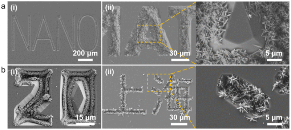 | ||
| Fig. 7 (a and b) SEM images of the TiO2 nanorod arrays with different features (scale bar marked in the figure). | ||
4. Conclusions
In summary, we report a hybrid method of micro/nano manufacturing in which a single crystal TiO2 nanorod array is grown in a multi-type mode substrate to meet the needs of arbitrary patterning. The combination of top-down photolithography and bottom-up hydrothermal treatment provided a simple and facile approach to complex patternization, which is of positive significance for the integration of microelectronic devices. The arbitrary patterns of substrate template are obtained through the lithographic pattern transfer process and wet-etching technology of silicon materials. Under the assistance of capillary force of microstructure angle, a certain amount of TiO2 seed precursor onto the template surface is gathered in the preset position to form a continuous patterning nucleation during subsequent calcination process. Then, TiO2 nanorod arrays are grown based on TiO2 crystallization seeds with various patterns in a controllable manner through conventional hydrothermal treatment. The microscopic morphology and density of the TiO2 nanorods could be adjusted by controlling the concentration of the seed precursor, hydrothermal reaction time and temperature, and the concentration of growth precursors. In conclusion, this work provides a promising approach to the low-cost and easy preparation of patterned TiO2 nanorod arrays with potential applications in optoelectronic devices, energy conversion, photocatalysis, and biomedicine in the future.Author contributions
Z. Ji and M. Sun contributed equally to this work. The experiments were designed by Z. Ji, B. Chen and X. Xu. Data were collected by Z. Ji and M. Sun, and analyzed by all authors. All of the authors contributed to the manuscript writing.Conflicts of interest
There are no conflicts to declare.Acknowledgements
This work is financially supported by the National Natural Science Foundation of China (Grant No. 51901159) and the Fundamental Research Funds for the Central Universities.Notes and references
- S. Dimov, E. Brousseau, R. Minev and S. Bigot, Proc. Inst. Mech. Eng., Part C, 2011, 226, 3–15 CrossRef.
- C. Chua, A. Loo and M. Pumera, Chemistry, 2016, 22, 14336–14341 CrossRef CAS PubMed.
- H. Wang, Y. Liu, M. Li, H. Huang, M. Zhong and H. Shen, Appl. Phys. A, 2009, 97, 25–29 CrossRef CAS.
- C. Chen, Y. Wei, G. Sun and B. Shao, Chem.–Asian J., 2012, 7, 1018–1025 CrossRef CAS PubMed.
- Y. Yuan, L. Han, D. Huang, J. Su, Z. Tian, Z. Tian and D. Zhan, Electrochim. Acta, 2015, 183, 3–7 CrossRef CAS.
- S. Gittard and R. Narayan, Expert Rev. Med. Devices, 2010, 7, 343–356 CrossRef PubMed.
- J. Fourkas, J. Phys. Chem. Lett., 2010, 1, 1221–1227 CrossRef CAS.
- H. Yu, M. Liao, W. Zhao, G. Liu, X. J. Zhou, Z. Wei, X. Xu, K. Liu, Z. Hu, K. Deng, S. Zhou, J. A. Shi, L. Gu, C. Shen, T. Zhang, L. Du, L. Xie, J. Zhu, W. Chen, R. Yang, D. Shi and G. Zhang, ACS Nano, 2017, 11, 12001–12007 CrossRef CAS PubMed.
- A. Carlson, A. M. Bowen, Y. Huang, R. G. Nuzzo and J. A. Rogers, Adv. Mater., 2012, 24, 5284–5318 CrossRef CAS PubMed.
- B. Wang, S. Shen and S. S. Mao, J. Materiomics, 2017, 3, 96–111 CrossRef.
- X. Chen, L. Liu, Z. Liu, M. A. Marcus, W. C. Wang, N. A. Oyler, M. E. Grass, B. Mao, P. A. Glans, P. Y. Yu, J. Guo and S. S. Mao, Sci. Rep., 2013, 3, 1510 CrossRef PubMed.
- X. Wang, Z. Li, J. Shi and Y. Yu, Chem. Rev., 2014, 114, 9346–9384 CrossRef CAS PubMed.
- Y. Zhu, L. Yang, J. Sheng, Y. Chen, H. Gu, J. Wei and Z. Zhou, Adv. Energy Mater., 2017, 7, 1701222 CrossRef.
- B. Liu, H. M. Chen, C. Liu, S. C. Andrews, C. Hahn and P. Yang, J. Am. Chem. Soc., 2013, 135, 9995–9998 CrossRef CAS PubMed.
- M. Wang, L. Sun, Z. Lin, J. Cai, K. Xie and C. Lin, Energy Environ. Sci., 2013, 6, 1211 RSC.
- C. Liu, L. Wang, Y. Tang, S. Luo, Y. Liu, S. Zhang, Y. Zeng and Y. Xu, Appl. Catal., B, 2015, 164, 1–9 CrossRef CAS.
- Q. Guo, C. Zhou, Z. Ma and X. Yang, Adv. Mater., 2019, 31, 1901997 CrossRef CAS PubMed.
- B. Roose, S. Pathak and U. Steiner, Chem. Soc. Rev., 2015, 44, 8326–8349 RSC.
- N. Wang, Z. Bai, Y. Qian and J. Yang, Adv. Mater., 2016, 28, 4126–4133 CrossRef CAS PubMed.
- H. Zhou and Y. Zhang, J. Phys. Chem. C, 2014, 118, 5626–5636 CrossRef CAS.
- X. Xu, J. Chen, S. Cai, Z. Long, Y. Zhang, L. Su, S. He, C. Tang, P. Liu, H. Peng and X. Fang, Adv. Mater., 2018, 30, 1803165 CrossRef.
- Y. Jing, A. Wang, J. Li, Q. Li, Q. Han, X. Zheng, H. Cao and S. Bai, Bio-Des. Manuf., 2021, 5, 153–162 CrossRef.
- K. Mcnamara and S. Tofail, Adv. Phys.: X, 2016, 2, 54–88 Search PubMed.
- G. Li, L. Wu, F. Li, P. Xu, D. Zhang and H. Li, Nanoscale, 2013, 5, 2118–2125 RSC.
- A. Mills, S. K. Lee, A. Lepre, I. P. Parkin and S. A. O'Neill, Photochem. Photobiol. Sci., 2002, 1, 865–868 CrossRef CAS PubMed.
- G. Zhang, H. B. Wu, T. Song, U. Paik and X. W. Lou, Angew. Chem., Int. Ed. Engl., 2014, 53, 12590–12593 CAS.
- M. Maria John, K. Ramamurthi, K. Sethuraman and R. Ramesh Babu, Appl. Surf. Sci., 2017, 405, 195–204 CrossRef CAS.
- L. Bazli, M. Siavashi and A. Shiravi, J. Compos. Compd., 2019, 1, 1–12 Search PubMed.
- J. Deng, J. Tao, T. Wu and H. Zhu, J. Mater. Sci.: Mater. Electron., 2011, 23, 295–301 CrossRef.
- X. Jiang, Q. Lin, Y. Zhang, K. Dong, Y. Zhang and Y. Shi, J. Mater. Sci.: Mater. Electron., 2017, 28, 12509–12513 CrossRef CAS.
- B. Çırak, Z. Demir, Ç. Eden, Y. Erdoğan, B. Caglar, S. Karadeniz, T. Kılınç, A. Ekinci and Ç. Çırak, J. Mater. Sci.: Mater. Electron., 2019, 30, 6335–6341 CrossRef.
- P. Fan, M. Zhong, B. Bai, G. Jin and H. Zhang, RSC Adv., 2016, 6, 45923–45930 RSC.
- L. Yang, D. Chu, L. Wang, G. Ge and H. Sun, Mater. Lett., 2016, 167, 4–8 CrossRef CAS.
- G. Kim, T. An and G. Lim, ACS Appl. Mater. Interfaces, 2017, 9, 19057–19062 CrossRef CAS PubMed.
- V. Mehta and S. N. Rath, Bio-Des. Manuf., 2021, 4, 311–343 CrossRef.
- X. Wang, Y. Tao, H. Zhao, M. Fu, D. He and Y. Wang, J. Alloys Compd., 2017, 704, 131–140 CrossRef CAS.
- L. Liu, Y. Wang, F. Sun, Y. Dai, S. Wang, Y. Bai, L. Li, T. Li, T. Zhang and S. Qin, Microsyst. Nanoeng., 2020, 6, 31 CrossRef CAS PubMed.
- H. Choi, Y. Lee, J. Yu, K. Hwang and J. Boo, Materials, 2016, 9, 656 CrossRef PubMed.
- Y. Hou, W. Wang and P. Bartolo, Bio-Des. Manuf., 2022, 5, 556–579 CrossRef.
- Z. Szabó, J. Volk, E. Fülöp, A. Deák and I. Bársony, Photon. Nanostruct: Fundam. Appl., 2013, 11, 1–7 CrossRef.
- W. Zhang, R. Zhu, V. Nguyen and R. Yang, Sens. Actuators, A, 2014, 205, 164–169 CrossRef CAS.
- Y. Xiong, M. Fang, Q. Zhang, W. Liu, X. Liu, L. Ma and X. Xu, J. Alloys Compd., 2022, 898, 163003 CrossRef CAS.
- T. Zhang, Z. U. Rahman, N. Wei, Y. Liu, J. Liang and D. Wang, Nano Res., 2017, 10, 1021–1032 CrossRef CAS.
- Z. Bai and Y. Zhang, J. Solid State Electrochem., 2016, 20, 3499–3505 CrossRef CAS.
- D. Baiyila, X. Wang, X. Li, B. Sharileaodu, X. Li, L. Xu, Z. Liu, L. Duan and J. Liu, J. Mater. Chem. A, 2014, 2, 12304–12310 RSC.
- J. Xiong, Z. Luo, J. Yang, Y. Guo, A. Piyadasa, S. Wang, S. Hoang, Y. Fang, S. Hu, W. Yang, H. Deng, L. Zhang and P.-X. Gao, CrystEngComm, 2019, 21, 2727–2735 RSC.
- W. Wang, J. Dong, X. Ye, Y. Li, Y. Ma and L. Qi, Small, 2016, 12, 1469–1478 CrossRef CAS PubMed.
- H. Chen, H. Chen, Z. Huang and D. Chen, Mater. Lett., 2014, 124, 275–278 CrossRef CAS.
- S. Karim, S. Nadzirah, J. Kazmi, R. Rahim, C. Dee, A. Hamzah and M. Mohamed, J. Mater. Sci., 2021, 56, 15344–15353 CrossRef.
- H. Zhou, P. Liu, Z. Gao, Q. Li, W. Lv, J. Yin, B. Zhang, H. Yang and L. Ma, Bio-Des. Manuf., 2022, 5, 433–436 CrossRef.
- M. Sun, C. Wang, M. Lv, Z. Fan and J. Du, J. Am. Chem. Soc., 2022, 144, 7337–7345 CrossRef CAS PubMed.
- J. Wang, Z. Ji, X. Xu, T. Chen, B. Chen, G. Gao, J. Ma, X. Nie and X. Xu, ACS Omega, 2022, 7, 22039–22045 CrossRef PubMed.
- Z. Ji, X. Liu, Y. Song, Y. Zhong, D. Wang, B. Chen, M. Fang, X. Nie, J. Hou, J. Ma, H. Ma, X. Xu, Z. Yi and X. Xu, J. Colloid Interface Sci., 2023, 630, 436–443 CrossRef CAS PubMed.
- H. Choi, E. Stathatos and D. D. Dionysiou, Appl. Catal., B, 2006, 63, 60–67 CrossRef CAS.
- M. Maria Angelin Sinthiya, N. Kumaresan, K. Ramamurthi, K. Sethuraman, B. S. Moorthy, B. R. Ramesh and V. Ganesh, Appl. Surf. Sci., 2018, 449, 122–131 CrossRef.
- H. Lu, Y. Zhou, S. Vongehr, S. Tang and X. Meng, Sci. China: Technol. Sci., 2012, 55, 894–902 CrossRef CAS.
- M. Maddah, C. P. Unsworth and N. O. V. Plank, Mater. Res. Express, 2018, 6, 015905 CrossRef.
Footnote |
| † Electronic supplementary information (ESI) available. See DOI: https://doi.org/10.1039/d3ra01423a |
| This journal is © The Royal Society of Chemistry 2023 |