
 Open Access Article
 This Open Access Article is licensed under a Creative Commons Attribution-Non Commercial 3.0 Unported Licence
Strain relaxation in monolayer MoS2 over flexible substrate†
Nilanjan Basu‡
 ab,
Ravindra Kumar‡ab,
D. Manikandanabc,
Madhura Ghosh Dastidarabd,
Praveen Hedgead,
Pramoda K. Nayak*abce and
Vidya Praveen Bhallamudi*ad
ab,
Ravindra Kumar‡ab,
D. Manikandanabc,
Madhura Ghosh Dastidarabd,
Praveen Hedgead,
Pramoda K. Nayak*abce and
Vidya Praveen Bhallamudi*ad
aDepartment of Physics, Indian Institute of Technology Madras, Chennai 600 036, India. E-mail: pramoda.iitm@gmail.com; praveen.bhallamudi@iitm.ac.in
b2D Materials Research and Innovation Group, Indian Institute of Technology Madras, Chennai 600 036, India
cMicro Nano and Bio-Fluidics Group, Indian Institute of Technology Madras, Chennai 600 036, India
dQuantum Center of Excellence for Diamond and Emerging Materials (QuCenDiEM) Group, Departments of Physics and Electrical Engineering, Indian Institute of Technology Madras, Chennai 600036, India
eCentre for Nano and Material Sciences, Jain (Deemed-to-be University), Jain Global Campus, Kanakapura, Bangalore, Karnataka 562112, India
First published on 31st May 2023
Abstract
In this communication, we demonstrate uniaxial strain relaxation in monolayer (1L) MoS2 transpires through cracks in both single and double-grain flakes. Chemical vapour deposition (CVD) grown 1L MoS2 has been transferred onto polyethylene terephthalate (PET) and poly(dimethylsiloxane) (PDMS) substrates for low (∼1%) and high (1–6%) strain measurements. Both Raman and photoluminescence (PL) spectroscopy revealed strain relaxation via cracks in the strain regime of 4–6%. In situ optical micrographs show the formation of large micron-scale cracks along the strain axis and ex situ atomic force microscopy (AFM) images reveal the formation of smaller lateral cracks due to the strain relaxation. Finite element simulation has been employed to estimate the applied strain efficiency as well as to simulate the strain distribution for MoS2 flakes. The present study reveals the uniaxial strain relaxation mechanism in 1L MoS2 and paves the way for exploring strain relaxation in other transition metal dichalcogenides (TMDCs) as well as their heterostructures.
1. Introduction
TMDCs are considered to be an exciting class of layered materials.1–4 One layer of a TMDC comprises X–M–X stacking, where X is a chalcogen and M is a metal atom. Across many applications of this type of two-dimensional (2D) material, strain engineering is becoming prominent. The effect of strain on 2D materials has a multifold effect on their surface morphology and properties. Strain can give rise to wrinkles, cracks, and interlayer dislocations in 2D materials including TMDCs. Strain modulation in TMDCs has been well reported in the literature, with reports available for both uniaxial and biaxial strain modulation in 2D materials/TMDCs like MoS2, WSe2, WS2, MoSe2, MoTe2, and many more.5–9 TMDCs show very small bending rigidity and a high Young's modulus, which makes them the perfect choice for bendable electronics.10,11 In addition, strain is also important for other applications such as single photon emission, optoelectronics, wearable electronics, piezoelectric sensors and moiré pattern studies.12–15 The study of strain relaxation and strain threshold over the transfer characteristics of MoS2 and other TMDCs is particularly important for flexible electronics where a lot of repeated deformation takes place. For these applications, it is crucial to identify the strain regime where strain relaxation starts to appear and its associated mechanisms. However, such studies in TMDCs are in a nascent stage.Strain can be introduced in TMDCs in multiple ways, which can be classified into two broad categories such as in situ synthesis and post-synthesis. During the in situ-synthesis process, strain can be generated by exploiting the lattice and thermal expansion coefficient mismatch between the substrate and the as-grown TMDCs.16–18 Whereas, the post-synthesis process is carried out by transferring the as-grown 2D material over flexible, patterned, and piezoelectric substrates for strain generation.19–22 Strain is also generated during the wet transfer process due to the formation of bubbles at the interface between the 2D material and substrate.23
Raman and PL spectroscopy are the two major non-destructive tools for studying strain modulation. The in-plane Raman mode in a TMDC is more sensitive to uniaxial strain compared to the out-of-plane mode. The shift in the in-plane Raman is due to the anharmonicity of the molecular potential.24 Several studies have focussed on band gap modulation and direct to the indirect transition of band gap with the applied strain in low regime (0–1%).25,26 For both low and high strain regimes, the band gap decreases linearly with the increase in strain. The behavior of the Raman phonon mode and PL spectra in a high-strain regime has also been reported and shows the signature of strain relaxation after a certain point.27,28 Molybdenum disulphide (MoS2) is an interesting and well-studied member of the TMDC family. The odd layer of MoS2 exhibits broken inversion symmetry and shows one of the highest piezo responses in monolayer TMDCs.29,30 This property propels for application in strain sensing, piezotronics, flexible optoelectronics, and nanocomposites.31,32 These applications inevitably require a comprehensive understanding of the strain effect over the band structure of MoS2 and also about strain relaxation mechanisms. In 2018 Niehues et al. reported the effect of strain (0–1.6%) over polycrystalline CVD grown MoS2 and studied the strain transfer process across the grain boundaries.33 Apart from this, there are substantial number of reports currently available about strain engineering in single layer MoS2 over flexible substrates, but only a hand full of publications report about strain relaxation mechanism in MoS2.27,34,35 Nevertheless, there is still a considerable research gap in the strain relaxation mechanism and identification of the strain regime where relaxation starts. In this present work, we have investigated the strain relaxation process of monolayer CVD grown single and double grain MoS2 flakes transferred onto flexible substrates like PET and PDMS, and highlighted the role of cracks during strain-relaxation. Finite element simulation has been carried out to estimate the strain efficiency of both the flexible substrates and the strain distribution of MoS2 flakes over them.
2. Results and discussion
2.1. Strain modulation
CVD-grown monolayer MoS2 flakes on (SiO2/Si) substrate is transferred over 125 μm thick PET substrate for strain modulation in 0–1% strain regime. The strain measurement has been carried out similar to that reported in ref. 36 and has been discussed in the ESI (Fig. S1).† Fig. 1(a) shows the optical micrograph of the as grown MoS2 on SiO2/Si substrate (monolayer characterization has been given in Fig. S2†). Fig. 1(b and c) shows the PL and Raman spectra of the transferred 1L MoS2 over PET under a low strain (0 to 0.82%). The PL spectra show that there is a gradual red shift, which implies the reduction of the direct band gap with the increase in strain (Fig. 1(e)). The linear fit in Fig. 1(e) gives a modulation efficiency of 52 meV/%, which is in agreement with the reported literature for monolayer MoS2.37 The shift in the optical band gap with strain is due to the increase in the valence band maxima position, although the conduction band minima position remains stable.38 The in-plane mode (E12g) in the Raman spectra (Fig. 1(b)) also shows a gradual red shift. The out-of-plane mode (A1g) is less sensitive to the applied uniaxial strain. The in-plane mode shows a redshift of 4.67 cm−1/% strain and the out-of-plane mode shows a much smaller redshift of 0.848 cm−1/%, which is consistent with the literature.25 As the applied strain is in-plane in nature, the E12g mode is more sensitive to the in-plane strain compared to the A1g mode. Both the PL and Raman spectra and in situ optical micrograph (shown in Fig. S2(c)†) do not show any signature of strain relaxation.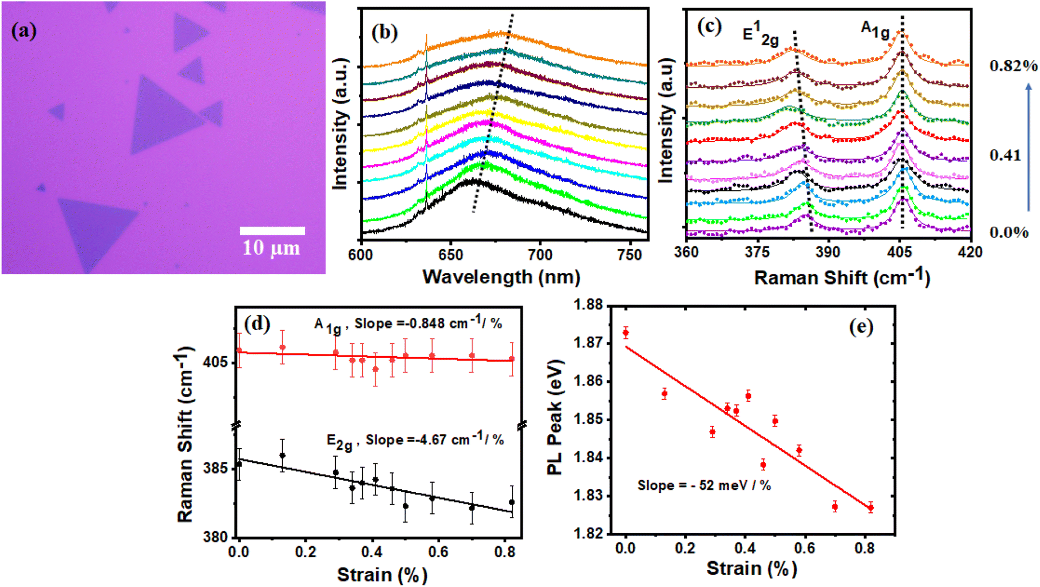 | ||
| Fig. 1 Raman, PL spectra under strain over PET. Optical micrograph (a) of as-synthesized 1L MoS2 over SiO2/Si, (b) and (c) PL & Raman spectra of 1L MoS2 under low strain over PET. (d) and (e) Raman & PL peak shift with respect to the strain percentage. | ||
In order to study this effect, a further increase in strain has been achieved by transferring 1L MoS2 over a 2 mm thick flexible PDMS substrate. For this study, a monolayer double grain butterfly like MoS2 flake has been chosen. Fig. 2(a) and (b) shows the PL and Raman spectra of monolayer MoS2 over PDMS under 0 to 6.2% strain. The absence of B exciton in the PL spectra can be attributed to the fact that the polymers substrates used to generate strain inhibits the B exciton intensity, which is analogous to other reports.39–41 The ex situ optical image of the particular double grain butterfly like flake (after application of strain) is shown in Fig. 2(c). The PL and Raman shift (E12g) with strain is shown in Fig. 2(a and b). The PL spectra with strain variation show a red shift up to 3.85% strain and on further increasing the strain, a blue shift is observed. This blue shift gradually continues up to 5.52% and 6.2% compared to the A exciton peak at 0% strain. The MoS2 film is completely relaxed at 6.2%.
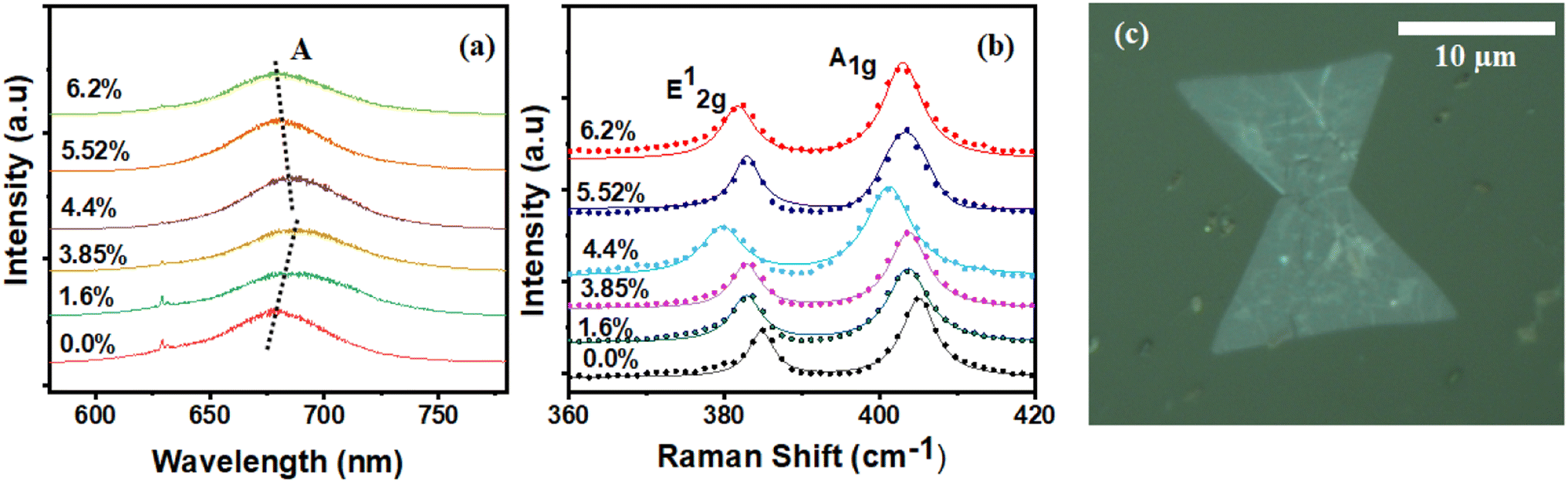 | ||
| Fig. 2 Raman and PL spectra under strain over PDMS. (a) PL spectra of 1L MoS2 under strain over 2 mm thick PDMS. (b) Raman spectra of the same flake under strain (c) ex situ optical micrograph of the particular flake after strain modulation. | ||
The Raman spectra of the butterfly shaped flake also show strain relaxation but at a slightly different strain value. After a gradual red shift up to 4.4% strain, the E12g peak undergoes a blue shift at 5.52% strain indicating the relaxation process. There is a slight difference of ∼1% strain between the strain relaxation point in PL and Raman spectra, which can be attributed to the fact that the electronic band structure is more sensitive to the applied strain than lattice vibrational modes. Apart from the double grain flake, the effect of strain over single grain triangular flake has also been investigated (Fig. S3†). The single grain triangular flake also behaves in a similar manner to the double grain flake, as shown in Fig. 2(c).
The strain relaxation commences at 4.4% strain for both the morphologies and this strain regime for the strain relaxation of monolayer MoS2 well matches in accordance with recent literature (Fig. 3).27 It has been reported that breaking occurs at 6–11% strain for a suspended monolayer exfoliated MoS2, which is slightly higher than our result.42 This difference can be attributed to the effect of the polymer substrate. Although the relaxation starts at a similar strain for both the flakes, the triangular flake attains a relaxed state at a lower strain than the double grain flake. The defects, vacancy states, dislocations, and structural imperfections of the MoS2 film also affect the strain relaxation process. Further focused studies are required to identify these effects and to establish a correlation between them (Fig. 3).
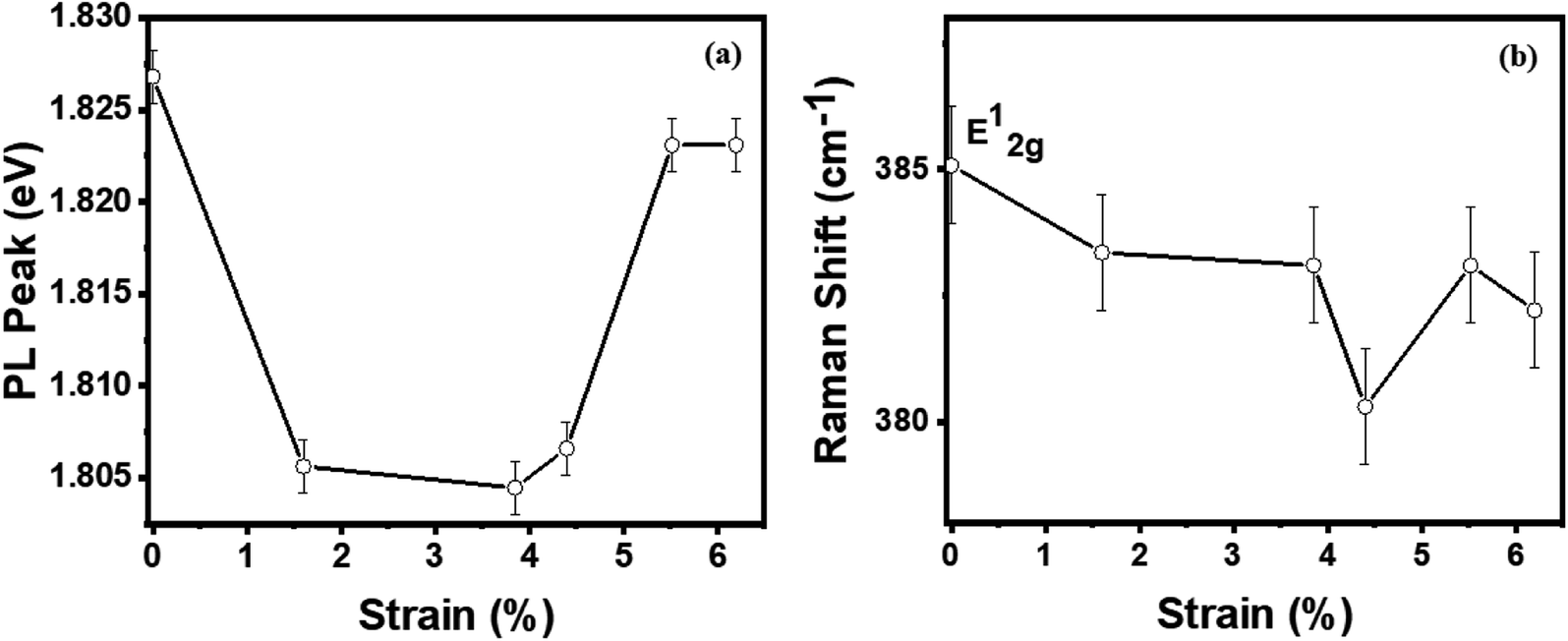 | ||
| Fig. 3 PL peak shift vs. strain (a) and Raman peak shift vs. strain (b) of the double grain MoS2 flake. | ||
Fig. 4(a) shows the in situ optical micrograph (recorded during PL & Raman measurement at 4.4% strain) and Fig. 4(b) shows ex situ (recorded after application of strain) atomic force microscopy (AFM) image. The grain boundary can be clearly seen in the AFM image. The distinctly visible cracks in the optical micrographs indicate that the strain relaxation is actuated by the formation of cracks in the MoS2 film. Owing to the limited resolution of the optical microscope, only the large cracks along the strain axis are visible. A closer inspection with AFM shows that other small lateral wrinkles also formed during the relaxation process. Wrinkle formation is also evident in triangular flakes as shown in Fig. S4.† Fig. 4(c) shows the height profile through a wrinkle of the double-grain flake, which shows a height of 17 nm. Wrinkles with variable sizes starting from 4 nm to as large as 26 nm are observed (Fig. S4†). Cracks and wrinkles of similar dimensions have also been reported in WS2 as the mode of strain relaxation.28 The AFM images (both Fig. 4 and S4†) have been recorded under relaxed conditions after the application of strain. The wrinkles displayed in the images indicate that there is a permanent change in the surface morphology of the MoS2 flakes. Cracks are also observed during the synthesis process of polycrystalline MoS2 and MoSe2 and MoS2 alloy as a way of strain relaxation during the synthesis process.33,35 For our as synthesized MoS2 flakes over SiO2/Si substrate, we have not observed any cracks (Fig. S2†). Generally, cracks and grain boundaries are more common in a polycrystalline MoS2 film. When subjected to strain a polycrystalline film with cracks exhibits a similar PL shift to that of a single grain flake.33 This is because each crack behaves as an independent edge and strain propagation is almost seamless across cracks. Despite this similarity, as synthesized film with cracks is not suitable for strain relaxation studies. As cracks already present in the film make it difficult to study strain relaxation in a controlled way.
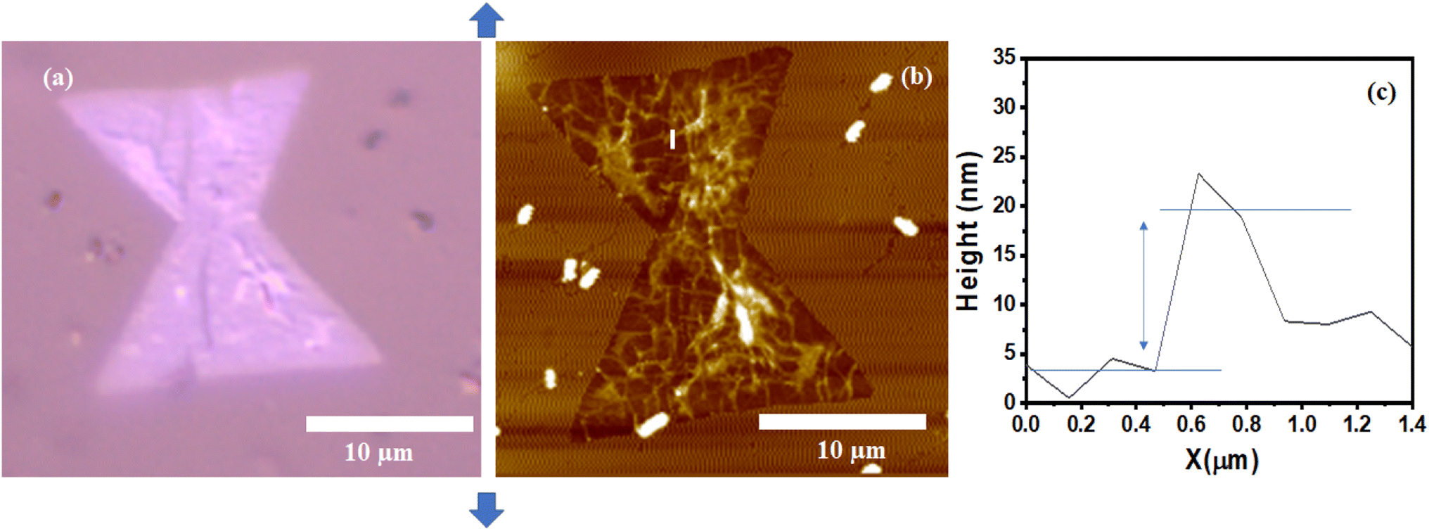 | ||
| Fig. 4 AFM and optical micrograph of the double grain flake. In situ optical micrograph (a) of the MoS2 flake under 4.4% strain and (b) ex situ AFM of the flake over PDMS. (c) The height profile of the wrinkle (in (b), shown by a white line) shows 17 nm height. The arrows indicate the strain axis. | ||
2.2. Finite element simulation
Further, to understand the strain transfer efficiency of the substrate, we have carried out the finite element simulations using COMSOL Multiphysics 6.0 (see Methods section). The schematic diagram of the MoS2 flakes transferred over the PDMS substrate used in our simulations is shown in Fig. 5(a). Fig. 5(b and c) shows the strain distribution on the MoS2 flakes (both single and double grain) for the three different applied strains on the PDMS substrate. Because of the significant difference in the Young's modulus values of the substrate and flake, the strain distribution is not uniform, and a small amount of strain is transferred to the flakes (Fig. 5(d)) similar to that reported in earlier studies.28,31,32,37,38,41,43 | ||
| Fig. 5 Finite element simulation of 1L MoS2 over PDMS. (a) Schematics of the 1L MoS2 deposited on the PDMS substrate before and after bending. The strain distribution on single grain (b) and double grain (c) 1L MoS2 for the applied strain of 1%, 3%, and 5%, respectively. (d) Maximum strain observed on the MoS2 vs. applied strain on the PDMS. (e) Percentage of transferred strain vs. Young's modulus of substrate. | ||
The strain distribution on the flake depends on the orientation and its size. The double-grain flake shows more transferred strain than the single flake due to its large area of contact with the PDMS substrate. Fig. S6† shows the strain distribution on the MoS2 flakes for the different strains over PET substrate. We observe the uniform distribution of the strain throughout the flake, and also, ∼97% of the applied strain is transferred to the flakes. To get more insights into the strain transfer efficiency of the substrate, we performed additional simulations by varying the substrate's Young's modulus value. The results show that the transfer efficiency follows sigmoidal variation with Young's modulus (Fig. 5(e)). Also, using the substrate with Young's modulus in the same order as that of the flake can result in an efficient strain transfer (more than 90%).8,25,26,28
3. Methods
3.1. Materials and growth
Witec alpha 300 Raman spectrometer was used for acquiring all Raman and PL spectra with a grating of 1800 lines per mm and a 50× objective (0.7 NA) with a spot size of ∼1 μm. The resolution of the Raman spectrometer was 1.3 cm−1 and the applied power was 3.5 mW. For all the spectra, the excitation wavelength was 532 nm. The Lorentzian function was used for fitting the Raman plots. To measure the thickness of the flakes Park systems NX10 AFM was used, with a tip radius less than 10 nm, force constant of 42 N m−1, and 330 kHz frequency. The AFM micrographs were recorded in non-contact mode. The optical micrographs were recorded by using a Nikon Eclipse LV100ND microscope.Single layer MoS2 was grown over 290 nm SiO2/Si in a two-zone atmospheric pressure CVD (APCVD). Sulphur (Sigma Aldrich, 99.98%) and molybdenum(IV) oxide (Alfa Aesar, 99%) was used as a precursor. 4 mg MoO3 was kept in an alumina crucible in the middle of zone one (825 °C) and 315 mg S was kept 35 cm upstream in zone two (285 °C). 100 SCCM Ar was used as a carrier gas and also for purging (15 min). The SiO2/Si was cleaned in acetone, isopropyl alcohol, and deionized water before loading into the growth chamber. Growth was carried out for 45 min in the presence of Ar atmosphere.
3.2. Transfer, strain measurement and simulation
The as-grown 1L MoS2 was transferred over PET/PDMS by using a wet transfer method.44 3.5 M KOH solution was used as an etchant and 3% polymethyl methacrylate (PMMA) was used as the top coating (spin-coated at 4000 rpm). Once transferred over PET/PDMS, the PMMA/MoS2 was air dried for 36 hours to reduce the chances of wrinkle formation. Finally, hot acetone (60 °C) was used to remove the top PMMA layer. A single axis micro stage with a resolution of 10 μm was used to bend the PET/PDMS (shown in Fig. S1†). The radius of curvature (R) and the thickness (2t) of PET/PDMS was used to calculate the generated strain.The finite element simulations of MoS2 (both single and double grain) flakes on PDMS/PET substrate were performed using COMSOL Multiphysics 6.0 software. Fig. 5(a) shows the schematic diagram of the MoS2 flake on the PDMS substrate before/under bending. Appropriate boundary conditions were applied to the substrate for simulating the 3-point bending. The perfect bonding condition is assumed between the substrate and the MoS2 flake. The complete system is discretized into 274![[thin space (1/6-em)]](https://www.rsc.org/images/entities/char_2009.gif) 897 to 550861 elements and the results reported are independent of mesh. Material properties used in these simulations are given in Table S1.†45–48
897 to 550861 elements and the results reported are independent of mesh. Material properties used in these simulations are given in Table S1.†45–48
4. Conclusion
The strain transfer efficiency is high for PET, but we did not observe any strain relaxation of the flakes in the case of PET substrate for the applied strain. In contrast, the MoS2 flake goes through strain relaxation on the PDMS substrate. As the calculated strain transfer efficiency is poor for the PDMS substrate with respect to its Young modulus, we used a thicker PDMS film (2 mm thick, Fig. S1†) to generate a strain of 6%. We attribute the strain relaxation to the formation of the wrinkles and cracks on the flakes due to the significant difference in Young's modulus of the substrate and flakes.28,41 The formation of wrinkles on the flakes affects their ultimate tensile strength resulting in the cracking of the flakes. From finite element simulations, it is evident that the crack of the flakes starts at the location where maximum strain is observed and propagates towards the gradient of strain inside the flakes (Fig. 4, 5 and S3†). However, the formation of the wrinkles on the flakes is entirely random.In summary, a series of uniaxial strain modulation studies were performed over mono layer single and double-grain MoS2. The applied strain varied from 0–6.2%, in which PET substrate was used for a low strain regime and PDMS for a higher strain regime. Our results show that monolayer MoS2 displays signs of strain relaxation between 4 to 6% strain. Further in situ optical micrographs and ex situ AFM images show that the relaxation is accompanied by the formation of cracks. These cracks formed both along the strain axis and also perpendicular to the strain axis. The applied strain in monolayer MoS2 relaxes by forming cracks. 3D finite element simulations were also performed, which showed that the Young modulus of the flexible substrate plays an important role in the strain transfer efficiency between the MoS2 flake and substrate. Also, the simulated propagation direction of the cracks well matched the experimental results. The authors hope that this work would provide a comprehensive understanding of the strain relaxation mechanism and strain threshold in MoS2 and that this study can be extended to other TMDCs as well.
Author contributions
Nilanjan Basu performed the growth,experiments and characterization, analyzed the data and wrote the manuscript. Ravindra Kumar performed experiments, Madhura Ghosh Dastidar and Praveen Hedge performed characterization. D. Manikandan did the simulation and wrote manuscript. Pramoda K. Nayak and Vidya Praveen Bhallamudi provided helpful discussions and reviewed the manuscript. All authors have given approval to the final version of the manuscript.Conflicts of interest
The authors declare no conflict of interest.Acknowledgements
V. P. B. and P. K. N. acknowledge MHRD STARS research grant [STARS/APR2019/396]. P. K. N. acknowledges the financial support from the Department of Science and Technology, Government of India (DST-GoI), with sanction Order No. SB/S2/RJN-043/2017 under Ramanujan Fellowship. P. K. N. also acknowledges the support from the Institute of Eminence scheme at IIT-Madras, through the 2D Materials Research and Innovation Group and Micro Nano Bio Fluidics Group. V. P. B. acknowledges the support from the Institute of Eminence scheme at IIT-Madras, through the Quantum Centers in Diamond and Emerging Materials (QuCenDiEM) group.This work is also partially supported by Jain University, Bangalore under minor research proposal grant (JU/MRP/CNMS/28/2022).Notes and references
- X. Yin, C. S. Tang, Y. Zheng, J. Gao, J. Wu, H. Zhang, M. Chhowalla, W. Chen and A. T. S. Wee, Chem. Soc. Rev., 2021, 50, 10087–10115 RSC.
- S. Manzeli, D. Ovchinnikov, D. Pasquier, O. V. Yazyev and A. Kis, Nat. Rev. Mater., 2017, 17033 CrossRef CAS.
- M. Ghosh Dastidar, I. Thekkooden, P. K. Nayak and V. Praveen Bhallamudi, Nanoscale, 2022, 14, 5289–5313 RSC.
- R. Rajarapu, P. K. Barman, R. Yadav, R. Biswas, M. Devaraj, S. Poudyal, B. Biswal, V. Laxmi, G. K. Pradhan, V. Raghunathan, P. K. Nayak and A. Misra, ACS Nano, 2022, 16, 21366–21376 CrossRef CAS PubMed.
- C. x. Yang, X. Zhao and S. y. Wei, Solid State Commun., 2016, 245, 70–74 CrossRef CAS.
- F. Carrascoso, H. Li, R. Frisenda and A. Castellanos-gomez, Nano Res., 2021, 14, 1698–1703 CrossRef.
- P. Kang, M. C. Wang, P. M. Knapp and S. W. Nam, Adv. Mater., 2016, 28, 4639–4645 CrossRef CAS PubMed.
- S. Yang, Y. Chen and C. Jiang, InfoMat, 2021, 3, 397–420 CrossRef.
- K. Parto, S. I. Azzam, K. Banerjee and G. Moody, Nat. Commun., 2021, 12, 1–8 CrossRef PubMed.
- K. Liu, Q. Yan, M. Chen, W. Fan, Y. Sun, J. Suh, D. Fu, S. Lee, J. Zhou, S. Tongay, J. Ji, J. B. Neaton and J. Wu, Nano Lett., 2014, 14, 5097–5103 CrossRef CAS PubMed.
- R. Roldán, A. Castellanos-Gomez, E. Cappelluti and F. Guinea, J. Phys.: Condens. Matter, 2015, 27, 313201 CrossRef PubMed.
- Q. Zhang, S. Zuo, P. Chen and C. Pan, InfoMat, 2021, 3, 987–1007 CrossRef CAS.
- J. Yao and G. Yang, J. Appl. Phys., 2020, 127, 030902 CrossRef CAS.
- J. P. So, H. R. Kim, H. Baek, K. Y. Jeong, H. C. Lee, W. Huh, Y. S. Kim, K. Watanabe, T. Taniguchi, J. Kim, C. H. Lee and H. G. Park, Sci. Adv., 2021, 7, 1–8 Search PubMed.
- S. K. Mallik, S. Sahoo, M. C. Sahu, A. K. Jena, G. K. Pradhan and S. Sahoo, J. Phys. Chem. C, 2022, 126, 15788–15794 CrossRef CAS.
- K. Tang and W. Qi, Adv. Funct. Mater., 2020, 30, 1–20 Search PubMed.
- F. Wang, B. Zhou, H. Sun, A. Cui, T. Jiang, L. Xu, K. Jiang, L. Shang, Z. Hu and J. Chu, Phys. Rev. B, 2018, 98, 1–9 Search PubMed.
- W. H. Chae, J. D. Cain, E. D. Hanson, A. A. Murthy and V. P. Dravid, Appl. Phys. Lett., 2017, 111, 143106 CrossRef.
- Y. Zhang, G. Gao, H. L. W. Chan, J. Dai, Y. Wang and J. Hao, Adv. Mater., 2012, 24, 1729–1735 CrossRef CAS PubMed.
- V. S. Mangu, M. Zamiri, S. R. J. Brueck and F. Cavallo, Nanoscale, 2017, 9, 16602–16606 RSC.
- S. T. Gill, J. H. Hinnefeld, S. Zhu, W. J. Swanson, T. Li and N. Mason, ACS Nano, 2015, 9, 5799–5806 CrossRef CAS PubMed.
- O. B. Aslan, I. M. Datye, M. J. Mleczko, K. Sze Cheung, S. Krylyuk, A. Bruma, I. Kalish, A. V. Davydov, E. Pop and T. F. Heinz, Nano Lett., 2018, 18, 2485–2491 CrossRef PubMed.
- A. V. Tyurnina, D. A. Bandurin, E. Khestanova, V. G. Kravets, M. Koperski, F. Guinea, A. N. Grigorenko, A. K. Geim and I. V. Grigorieva, ACS Photonics, 2019, 6, 516–524 CrossRef CAS.
- M. Huang, H. Yan, C. Chen, D. Song, T. F. Heinz and J. Hone, Proc. Natl. Acad. Sci. U. S. A., 2009, 106, 7304–7308 CrossRef CAS PubMed.
- Z. Li, Y. Lv, L. Ren, J. Li, L. Kong, Y. Zeng, Q. Tao, R. Wu, H. Ma, B. Zhao, D. Wang, W. Dang, K. Chen, L. Liao, X. Duan, X. Duan and Y. Liu, Nat. Commun., 2020, 11, 1151 CrossRef CAS PubMed.
- S. B. Desai, G. Seol, J. S. Kang, H. Fang, C. Battaglia, R. Kapadia, J. W. Ager, J. Guo and A. Javey, Nano Lett., 2014, 14, 4592–4597 CrossRef CAS PubMed.
- W. Zhang, F. Cheng, J. Huang, H. Yuan and Q. Wang, Phys. Lett. A: Gen. At. Solid State Phys., 2021, 418, 127709 CrossRef CAS.
- Q. Zhang, Z. Chang, G. Xu, Z. Wang, Y. Zhang, Z. Q. Xu, S. Chen, Q. Bao, J. Z. Liu, Y. W. Mai, W. Duan, M. S. Fuhrer and C. Zheng, Adv. Funct. Mater., 2016, 26, 8707–8714 Search PubMed.
- R. Hinchet, U. Khan, C. Falconi and S. W. Kim, Mater. Today, 2018, 21, 611–630 CrossRef CAS.
- W. Wu, L. Wang, Y. Li, F. Zhang, L. Lin, S. Niu, D. Chenet, X. Zhang, Y. Hao, T. F. Heinz, J. Hone and Z. L. Wang, Nature, 2014, 514, 470–474 CrossRef CAS PubMed.
- G.-H. Lee, Y.-J. Yu, X. Cui, N. Petrone, C.-H. Lee, M. S. Choi, D.-Y. Lee, C. Lee, W. J. Yoo, K. Watanabe, T. Taniguchi, C. Nuckolls, P. Kim and J. Hone, ACS Nano, 2013, 7, 7931–7936 CrossRef CAS PubMed.
- H. Zhu, Y. Wang, J. Xiao, M. Liu, S. Xiong, Z. J. Wong, Z. Ye, Y. Ye, X. Yin and X. Zhang, Nat. Nanotechnol., 2015, 10, 151–155 CrossRef CAS PubMed.
- I. Niehues, A. Blob, T. Stiehm, R. Schmidt, V. Jadriško, B. Radatović, D. Čapeta, M. Kralj, S. M. De Vasconcellos and R. Bratschitsch, 2D Mater., 2018, 5, 031003 CrossRef.
- D. J. Trainer, Y. Zhang, F. Bobba, X. Xi, S. W. Hla and M. Iavarone, ACS Nano, 2019, 13, 8284–8291 CrossRef CAS PubMed.
- H. Taghinejad, A. A. Eftekhar, P. M. Campbell, B. Beatty, M. Taghinejad, Y. Zhou, C. J. Perini, H. Moradinejad, W. E. Henderson, E. V. Woods, X. Zhang, P. Ajayan, E. J. Reed, E. M. Vogel and A. Adibi, npj 2D Mater. Appl., 2018, 2, 10 CrossRef.
- J. O. Island, A. Kuc, E. H. Diependaal, R. Bratschitsch, H. S. J. Van Der Zant, T. Heine and A. Castellanos-Gomez, Nanoscale, 2016, 8, 2589–2593 RSC.
- C. R. Zhu, G. Wang, B. L. Liu, X. Marie, X. F. Qiao, X. Zhang, X. X. Wu, H. Fan, P. H. Tan, T. Amand and B. Urbaszek, Phys. Rev. B: Condens. Matter Mater. Phys., 2013, 88, 121301 CrossRef.
- C. Chong, H. Liu, S. Wang and K. Yang, Nanomaterials, 2021, 11(11), 3127 CrossRef CAS PubMed.
- H. J. Conley, B. Wang, J. I. Ziegler, R. F. Haglund, S. T. Pantelides and K. I. Bolotin, Nano Lett., 2013, 13, 3626–3630 CrossRef CAS PubMed.
- J. W. Christopher, M. Vutukuru, D. Lloyd, J. S. Bunch, B. B. Goldberg, D. J. Bishop and A. K. Swan, J. Microelectromech. Syst., 2019, 28, 254–263 CAS.
- Z. Liu, M. Amani, S. Najmaei, Q. Xu, X. Zou, W. Zhou, T. Yu, C. Qiu, A. G. Birdwell, F. J. Crowne, R. Vajtai, B. I. Yakobson, Z. Xia, M. Dubey, P. M. Ajayan and J. Lou, Nat. Commun., 2014, 5, 5246 Search PubMed.
- S. Bertolazzi, J. Brivio and A. Kis, ACS Nano, 2011, 5, 9703–9709 CrossRef CAS PubMed.
- H. J. Kim, D. Kim, S. Jung, M. H. Bae, Y. J. Yun, S. N. Yi, J. S. Yu, J. H. Kim and D. H. Ha, J. Raman Spectrosc., 2018, 49, 1938–1944 CrossRef CAS.
- A. J. Watson, W. Lu, M. H. D. Guimaraes and M. Stöhr, 2D Mater., 2021, 8, 032001 CrossRef CAS.
- F. C. P. Sales, R. M. Ariati, V. T. Noronha and J. E. Ribeiro, Procedia Struct. Integr., 2021, 37, 383–388 CrossRef.
- S. Dogru, B. Aksoy, H. Bayraktar and B. E. Alaca, Polym. Test., 2018, 69, 375–384 CrossRef CAS.
- G. Casillas, U. Santiago, H. BarroÌn, D. Alducin, A. Ponce and M. José-Yacamán, J. Phys. Chem. C, 2015, 119, 710–715 CrossRef CAS PubMed.
- J. Kang, H. Sahin and F. M. Peeters, Phys. Chem. Chem. Phys., 2015, 17, 27742–27749 RSC.
Footnotes |
| † Electronic supplementary information (ESI) available. See DOI: https://doi.org/10.1039/d3ra01381b |
| ‡ Equally contributed to the work. |
| This journal is © The Royal Society of Chemistry 2023 |