
 Open Access Article
 This Open Access Article is licensed under a Creative Commons Attribution-Non Commercial 3.0 Unported Licence
Facile fabrication of gas sensors based on molybdenum disulfide nanosheets and carbon nanotubes by self-assembly†
Hyejin Rhyuac,
Seonjeong Leea,
Myunghyun Kangb,
Daeho Yoon c,
Sung Myung*a,
Wooseok Songa,
Sun Sook Leea and
Jongsun Lima
c,
Sung Myung*a,
Wooseok Songa,
Sun Sook Leea and
Jongsun Lima
aThin Film Materials Research Center, Korea Research Institute of Chemical Technology (KRICT), 141 Gajeong-ro, Yuseong-gu, Daejeon, 34114, Republic of Korea
bAdvanced Materials Division, Korea Research Institute of Chemical Technology (KRICT), 141 Gajeong-ro, Yuseong-gu, Daejeon 34114, Republic of Korea
cDepartment of Advanced Material Science and Engineering, Sungkyunkwan University, Suwon 16419, Republic of Korea
First published on 27th April 2023
Abstract
The rising importance of gas detection has prompted rigorous research on flexible and transparent high-performance gas sensors. We demonstrated a sensor for NO2 detection at room temperature, in which our device was fabricated via screen printing on a flexible substrate, and MoS2 and single-walled carbon nanotube (SWCNT) were coated on a specific area by the self-assembly method. This fabrication process is rapid, facile, and cost-effective. The proposed sensor enables precise and stable NO2 gas sensing from 50 ppb to 100 ppm. This method should also be applicable to the selective detection of other gases.
1 Introduction
Two-dimensional transition metal dichalcogenides (2D TMDs) have attracted immense research interest in recent years owing to their physical flexibility, unique 2D geometry, and high surface-to-volume ratio.1–4 In particular, 2D TMDs have shown great promise for use as chemical sensors because of their enhanced sensitivity and room-temperature gas-sensing ability in relation to conventional metal oxides, which generally require high operating temperatures.5–8 Among the 2D TMDs, MoS2 has been widely used in thin electronics because MoS2 nanosheets have unique physical and chemical properties such as optical transparency, flexibility, and tunable band gaps depending on their structure. MoS2 is a typical 2D TMD used for gas detection owing to its high surface-to-volume ratio, tunable band gap, and high adsorption coefficient.For application in electrical devices, MoS2 nanosheets have been synthesized via the exfoliation of bulky MoS2 or chemical vapor deposition through the sulfurization of molybdenum precursors.9–12 Recently, composites of polymers and 2D semiconducting nanostructures, such as those of MoS2, have been synthesized to overcome the sensitivity limitations of 2D TMD-based sensors.13–16 Because 2D carbon-based materials are highly sensitive to gases owing to their intrinsic electrical properties, hybrid layers based on 2D TMDs and graphene with high electron transfer rates and surface-to-volume ratios were utilized to enhance electrochemical and sensing behaviors.17–19
One-dimensional carbon nanostructures such as carbon nanotubes (CNTs), graphene oxide (GO), and reduced graphene oxide (rGO) were explored for application as gas sensors. Carbon-based materials have large surface areas for adsorbing gas molecules and high strength and stability.20–22 In addition, carbon-based materials such as single-walled carbon nanotubes (SWCNTs) were extensively studied as semiconductors for fabricating flexible and sensitive gas sensors, in which SWCNT-based networks are functionalized with polymers, oxide nanoparticles, and other compounds.23–25
NO2, which is emitted by fossil fuel consumption and diesel vehicles, is harmful to both humans and the environment, necessitating its efficient and cost-effective detection.26–29
In this study, NO2 gas sensors were fabricated via the selective assembly of nanostructures on the thermoplastic elastomers styrene-ethylene/butylene-styrene (SEBS) and polyurethane (PU), which are stretchable and intrinsically flexible.30–32 PU has a more hydrophilic surface than SEBS, which causes the MoS2 nanosheets and SWCNTs to selectively assemble on its surface. Therefore, PU patterns with a hydrophilic surface were utilized to assemble millions of MoS2/SWCNT nanosheets over large surface areas, while hydrophobic SEBS patterns were used to prevent any unwanted adsorption on nanostructures. Additionally, the MoS2/SWCNT nanosheets were placed uniformly over the PU surface. A metallic silver electrode was layered on the substrate using screen printing as well. Owing to the wide band gap and flexibility of the MoS2 nanosheets, the flexibility and gas detection performance of the gas sensors were improved through hybridization of the nanosheets with SWCNTs. The MoS2/SWCNT-based sensors exhibited NO2 gas sensitivities of up to 50 ppb at room temperature. As we only used screen printing and selective self-assembly for the fabrication of flexible gas sensors, this approach may lead to the facile industrial-level production of 2D TMD-based devices for practical applications.
2 Experimental
2.1 Synthesis and preparation of MoS2 nanosheets and SWCNTs
MoS2 was synthesized using the hydrothermal method. For the synthesis of MoS2 nanosheets, 1 g of sodium molybdate dihydrate (4.13 mmol) and 1 g of thioacetamide (13 mmol) were dissolved in deionized water (30 mL) and stirred for 30 min. The mixed solution was transferred to a Teflon-lined stainless-steel autoclave, where it underwent hydrothermal reaction at 180 °C for 2 h, after which it was cooled to 25 °C. The resulting suspension was centrifuged with deionized water and ethanol several times to remove the supernatant. The resulting black MoS2 nanosheets were dried overnight in a vacuum oven at 80 °C. Subsequently, 10 mg of MoS2 nanosheets, 4 mg of SWCNTs, and 20 mg of sodium dodecylbenzenesulfonate as the suspension agent were suspended in a solution of deionized water (10 mL).2.2 Fabrication of flexible MoS2/SWCNT-based gas sensor
SEBS was mixed with toluene in the mass ratio of 2![[thin space (1/6-em)]](https://www.rsc.org/images/entities/char_2009.gif) :5 and stirred for 24 h at room temperature. The solution was used to fabricate a 120 μm-thick SEBS layer on a polyethylene terephthalate (PET) substrate via bar coating using a 4-side applicator. The applicator can be used to adjust the thickness of SEBS. Further, PU was then dissolved in N,N-dimethylformamide (DMF) in the mass ratio of 1:4. PU patterns were fabricated on top of the SEBS layer by screen printing using shadow mask and squeeze in Fig. 1(b) and (c). MoS2 and SWCNTs were then spin-coated onto the PU and SEBS layers at 2000 rpm for 30 s in Fig. 1(d). Finally, as indicated in Fig. 1(f), the silver electrode was screen-printed on the PU with a channel of 1000 μm and a length of 100 μm shadow mask and squeeze.
:5 and stirred for 24 h at room temperature. The solution was used to fabricate a 120 μm-thick SEBS layer on a polyethylene terephthalate (PET) substrate via bar coating using a 4-side applicator. The applicator can be used to adjust the thickness of SEBS. Further, PU was then dissolved in N,N-dimethylformamide (DMF) in the mass ratio of 1:4. PU patterns were fabricated on top of the SEBS layer by screen printing using shadow mask and squeeze in Fig. 1(b) and (c). MoS2 and SWCNTs were then spin-coated onto the PU and SEBS layers at 2000 rpm for 30 s in Fig. 1(d). Finally, as indicated in Fig. 1(f), the silver electrode was screen-printed on the PU with a channel of 1000 μm and a length of 100 μm shadow mask and squeeze.
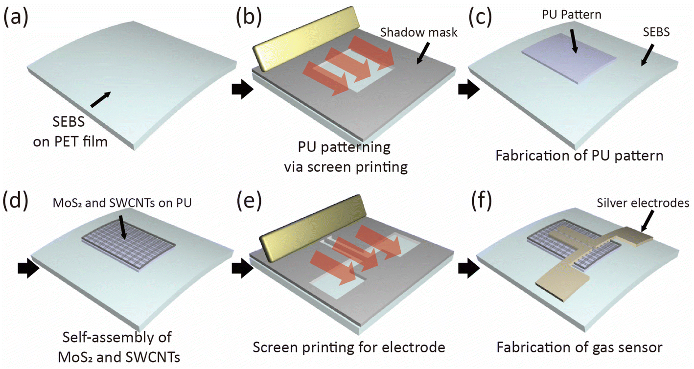 | ||
| Fig. 1 Schematic of the fabrication process of MoS2/SWCNT-based gas sensor. (a) Screen printing styrene-ethylene/butylene-styrene (SEBS) on a polyethylene terephthalate (PET) film. (b) Screen printing polyurethane (PU) through shadow mask on SEBS. (c) Fabrication of PU pattern. (d) MoS2/SWCNT on PU by self-assembly. (e) Screen printing for silver electrode. (f) Fabrication of MoS2/SWCNT gas sensor. | ||
2.3 Material characterization and gas-sensing measurements using MoS2/SWCNT-based gas sensors
The morphologies of the synthesized MoS2 nanosheets were investigated through transmission electron microscopy (TEM, Titan Cube G2 60-300, FEI company). X-ray diffraction (XRD, Rigaku) was conducted to identify the crystal phase of the synthesized MoS2 nanosheets with Cu–Kα radiation (λ = 1.5418 Å) at a current of 40 mA and voltage of 40 kV. For performing chemical-information Raman spectroscopy (inVia Raman spectroscope, Renishaw), X-ray photoelectron spectroscopy (XPS, K-alpha, Thermo Scientific) with an Al–Kα radiation (hν = 1486.6 eV) was used to examine the compositions of the MoS2 nanosheets. The morphological structures of the MoS2/SWCNT-based gas sensor samples were characterized by field-emission scanning electron microscopy (FE-SEM, Hitachi, S-4700) and energy-dispersive X-ray spectroscopy (EDS).The electrical properties of the sensors were measured using a semiconductor parameter analyzer (Keithley-4200, Keithley Instruments, USA). NO2, CO, H2S, NH3, acetone, and ethanol gases were individually injected into the sensing chamber to analyze the resistance of the sensors toward them; the sensors were placed 2 cm from the gas inlet, and gas-sensing measurements were carried out at room temperature and under 25% relative humidity.
3 Results and discussion
The screen-printing technique was used to fabricate a MoS2/SWCNT-based gas sensor, as illustrated in Fig. 1. In the first instance, a 120 μm-thick SEBS layer was fabricated on a PET substrate using the 4-side applicator (Fig. 1(a)). Next, the PU patterns were printed on top of the SEBS layer. When we spin-coated the mixture of MoS2 and SWCNTs onto the PU and SEBS patterns, we only observed the assembling of nanostructures on the PU pattern, which has a hydrophilic surface. The hydrophobic SEBS layer prevented adsorption on the SWCNTs. Then, Fig. 2(a)–(d) displays the results of the TEM, XRD, Raman spectroscopy and XPS analyses for the synthesized MoS2. As shown in Fig. 2(a(i)) the interlayer distance of the MoS2 nanosheets was approximately 0.65 nm, which corresponds to the (002) plane of bulk MoS2. The lattice d-spacing was estimated to be 0.25 nm, which corresponds to the (100) lattice plane of the MoS2 phase; this concurs with the XRD results. Fig. 2(a(ii)) MoS2 selected area electron diffraction (SAED) patterns indicating the hexagonal lattice structure of MoS2 nanosheets. Fig. 2(a(iii) and (iv)) displays crumpled MoS2 nanosheets with a size of hundreds of nanometers. | ||
| Fig. 2 (a) Transmission electron microscopy (TEM) images of MoS2 nanosheets: (i) TEM images of MoS2 show the lattice distance. (ii) Selected area electron diffraction (SAED) pattern. (iii and iv) TEM images of MoS2 nanosheets. (b) X-ray diffraction (XRD) patterns of MoS2 nanosheets (c) Raman spectra of MoS2. X-ray photoelectron spectroscopy (XPS) spectra of (d) Mo 3d and S 2p. | ||
Fig. 2(b) illustrates the XRD spectra of the MoS2 nanosheets; the characteristic peaks of the MoS2 nanosheets were observed at 11.52°, 33.90°, and 56.62°, corresponding to the (002), (100), and (110) planes, respectively. Fig. 2(c) represents the Raman spectra (λexc = 532 nm) displaying the signals for the in-plane vibrational mode (E12g) and out-of-plane vibrational mode (A1g) of MoS2 at 383.02 and 408.14 cm−1, respectively. Fig. 2(d) illustrates the XPS results for Mo 3d and S 2p. For Mo 3d, two strong peaks are located at 229.6 and 232.8 eV, which can be ascribed to Mo 3d5/2 and Mo 3d3/2. The small peak at 226.8 eV was assigned to the S 2s of MoS2. Other observed peaks at 162.4 and 163.6 eV were assigned to S in 2H–MoS2. This confirms the successful synthesis of MoS2.
Fig. 3(a) depicts the SEM images of PU and SEBS after the assembly of MoS2 and the SWCNTs. These results indicate that, upon spin coating, both MoS2 nanosheets and SWCNTs assembled selectively on the PU region, and SWCNTs could not be observed on the hydrophobic SEBS surface. Here, the density of MoS2/SWCNT adhering to the PU surface can be controlled by adjusting the concentration of the MoS2/SWCNT solution. The hydrophilic surface of PU adsorbed MoS2 and SWCNTs, and the hydrophobic SEBS layer repelled SWCNTs. The EDS measurements also confirmed the uniform assembly of MoS2/SWCNT network patterns on the PU substrate (Fig. 3(b)). The MoS2/SWCNT network on PU was composed of O, S, Mo, and C. Finally, a silver layer with a channel of 1000 μm and length of 100 μm was screen-printed on the PU surface. It acts as the conductive metallic layer required to complete the fabrication of the MoS2/SWCNT-based gas sensors. As indicated in the SEM images and EDS analyses of PU and SEBS boundary after the assembly of MoS2 and the SWCNTs, MoS2 nanosheets were assembled on both PU and SEBS, whereas the SWCNTs were observed only on PU (Fig. S1 in ESI†). Additionally, the MoS2/SWCNT assembled on PU was analyzed by using XPS in order to confirm the chemical state and bonding of MoS2/SWCNT in Fig. S2 in ESI.†
 | ||
| Fig. 3 (a) Scanning electron microscopy (SEM) images of MoS2/SWCNT on PU and SEBS: (i) SWCNTs self-assembly on PU (ii) MoS2/SWCNT self-assembly on PU (iii) SWCNTs on SEBS (iv) MoS2/SWCNT on SEBS (b) energy dispersive spectroscopy (EDS) elemental mapping of MoS2/SWCNT O, S, Mo, and C elements on PU substrate. | ||
Fig. 4(a) shows the response of the sensor to 100 ppm NO2 observed during the two testing cycles at room temperature; the cyclic nature of the response demonstrates the sensor's repeatable gas response and recovery in Fig. S3 in ESI.† It is well-known that, in the presence of MoS2 and SWCNTs, NO2 acts as an electron acceptor while NH3 acts as an electron donor. These results clearly demonstrated the enhanced response of the MoS2/SWCNT system to both NO2 and NH3, in which the resistance of the device decreased with NO2 adsorption and increased with NH3 adsorption. In previous reports, p-type carbon materials, such as graphene or SWCNTs functionalized with n-type MoS2 nanosheets were found to behave as p-type materials. Similarly, the analyses led us to conclude that the proposed MoS2/SWCNT hybrid structure was a p-type semiconductor material. The sensing mechanism of the NO2 gas-sensor MoS2/SWCNT was explained as in previous references. As NO2 gathers a free electron from the MoS2 and SWCNTs, MoS2/SWCNT exhibits p-type semiconductor properties. The two components cause the generation of more holes when hybridized. Hence, when the sensor was exposed to NO2, its resistance decreased and sensitivity increased. We performed a cycling test to evaluate the stability of the gas sensors in Fig. 4(a). The curves exhibited reproducible responses when air and NO2 were injected alternately. The sensor exhibited a sensitivity of 88% to 100 ppm of NO2 at room temperature. The gas sensitivity was calculated as ΔR/Ra = (Rg − Ra)/Ra, where Ra and Rg are the resistances of the sensor to synthetic air and the target gas, respectively.14,33–35
 | ||
| Fig. 4 The response of NO2 gas at room temperature. (a) Two successive sensing responses at NO2 100 ppm, (b) dynamic responses and recovery curves of MoS2/SWCNT gas sensor towards NO2 gas at room temperature (c) fitting curve of response versus concentration. | ||
At various NO2 concentrations, the detection limit for NO2 gas ranged from 50 ppb to 1 ppm (Fig. 4(b)). In Fig. 4(b), detection of 50 ppb of NO2 can be regarded as the minimum detection limit of the MoS2/SWCNT gas sensor, with a response value of 4.5%. These results indicate good performance compared to other studies for NO2 gas sensors using MoS2 and graphene hybrid materials in Table S1 in ESI.† When the concentration was increased from 50 ppb to 1 ppm, the response increased proportionally (Fig. 4(c)). As the relationship between concentration and sensitivity was linear, we concluded that the structure of the nanomaterial did not affect the sensing performance; therefore, the proposed fabrication method can be used with any nanoscale material, including nanowires, nanotubes, and nanoparticles. The response of the MoS2/SWCNT-based gas sensor to various other gases (CO, H2S, NH3, acetone vapor, and ethanol vapor) at room temperature was also investigated (Fig. 5). We tested 100 ppm of a specific gas at room temperature in two cycles. The responses to CO, H2S, and NH3 were 2.6%, 7.8%, and 14.8%, respectively, with no response to acetone or ethanol gases in Fig. 5(a)–(e). In contrast to the resistance change caused by NO2, the resistance of the MoS2/SWCNT-based gas sensor to NH3 and H2S gases increased with the adsorption of their molecules. This is because NO2 accepts electrons, whereas NH3 and H2S act as electron donors. The response value of 100 ppm NO2 was 11.3 times that of 100 ppm H2S and 5.9 times that of 100 ppm NH3 (Fig. 5(f)). This substantiates the gas sensor's excellent selectivity to NO2 at room temperature.
 | ||
| Fig. 5 Gas response performance of MoS2/SWCNT sensor at room temperature 100 ppm. (a) CO gas response, (b) H2S gas response, (c) NH3 gas response, (d) acetone gas response, (e) ethanol gas response, and (f) gas selectivity summary of the sensor to various gases at room temperature. | ||
As illustrated in Fig. 4, the response of the sensor decreases for NO2 gas. First, the material is exposed to air, and O2 molecules are adsorbed and form O2− ions on the material surface.
| O2 (g) + e− → O2− (ads) |
Upon exposure to the material, NO2 gas becomes NO2− by accepting electrons from the O2− ions.
| NO2 (g) + e− → NO2− (ads) |
| NO2 (g) + O2− (ads) + 2e− → NO2− (ads) + 2O− |
This confirms that the gas-sensing material increased the concentration of holes on the surface of the material. As shown in Fig. 5(c), the transient resistance responses of the sensor to NO2 and NH3 were compared. In contrast to the resistance change caused by NO2, the resistance increased when exposed to NH3 because the MoS2/SWCNT sensor is a p-type semiconductor.
| O2 (g) + e− → O2− (ads) |
| 2NH3 (ads) + 3O2− → N2 (g) + 3H2O + 3e− |
| NH3 (ads) + OH− → NH2 + H2O + e− |
When the MoS2/SWCNT-based sensor was exposed to NH3, following this mechanism, the O species reacted with NH3. Then the electrons were released back to MoS2/SWCNT, causing an increase in the electron concentration in the conduction band of MoS2. The transferred electrons recombined with the carriers, thus decreasing the charge carrier concentration and consequently increasing the electrical resistance.34–36 Therefore, owing to the synergistic actions of MoS2 and SWCNTs, the MoS2/SWCNT-based gas sensor exhibited high sensitivity to NO2 gas.
4 Conclusions
We demonstrated a facile method of fabricating high-performance MoS2/SWCNT-based gas sensors via screen printing, making it a rapid, simple, and cost-effective technology. While MoS2 assembled itself on both SEBS and PU, the SWCNTs attached only to the hydrophilic PU; therefore, MoS2/SWCNT hybrid nanostructures were successfully assembled on PU substrates. The MoS2/SWCNT-based gas sensor exhibited high selectivity for NO2 at room temperature, as well as high performance, reliable response, and recovery. In particular, the response to 100 ppm NO2 at room temperature was 11.3 and 5.9 times higher than that to 100 ppm H2S and NH3, respectively. Moreover, the hybrid gas sensor was fabricated on a flexible substrate; therefore, it should be applicable in sensitive wearable electronics.Conflicts of interest
There are no conflicts to declare.Acknowledgements
This research was supported by the Nanomaterial Technology Development Program through the National Research Foundation of Korea (NRF) funded by the Ministry of Science and ICT (NRF-2021M3H4A3A02086431).Notes and references
- M. Chhowalla, H. S. Shin, G. Eda, L.-J. Li, K. P. Loh and H. Zhang, Nat. Chem., 2013, 5, 263–275 CrossRef PubMed.
- K. F. Mak and J. Shan, Nat. Photon., 2016, 10, 216–226 CrossRef CAS.
- J. W. Seo, Y. W. Jun, S. W. Park, H. Nah, T. Moon, B. Park, J. G. Kim, Y. J. Kim and J. Cheon, Angew. Chem., Int. Ed., 2007, 46, 8828–8831 CrossRef CAS PubMed.
- M. Chhowalla, Z. Liu and H. Zhang, Chem. Soc. Rev., 2015, 44, 2584–2586 RSC.
- K. Lee, R. Gatensby, N. McEvoy, T. Hallam and G. S. Duesberg, Adv. Mater., 2013, 25, 6699–6702 CrossRef CAS PubMed.
- K. Y. Ko, J.-G. Song, Y. Kim, T. Choi, S. Shin, C. W. Lee, K. Lee, J. Koo, H. Lee and J. Kim, ACS Nano, 2016, 10, 9287–9296 CrossRef CAS PubMed.
- X. Liu, T. Ma, N. Pinna and J. Zhang, Adv. Funct. Mater., 2017, 27, 1702168 CrossRef.
- S. Hussain, A. J. Khan, M. Arshad, M. S. Javed, A. Ahmad, S. S. A. Shah, M. R. Khan, S. Akram, S. Ali and Z. A. ALOthman, Ceram. Int., 2021, 47, 8659–8667 CrossRef CAS.
- F. K. Perkins, A. L. Friedman, E. Cobas, P. M. Campbell, G. G. Jernigan and B. T. Jonker, Nano Lett., 2013, 13, 668–673 CrossRef CAS PubMed.
- L.-C. Wang, S.-K. Bao, J. Luo, Y.-H. Wang, Y.-C. Nie and J.-P. Zou, Int. J. Hydrogen Energy, 2016, 41, 10737–10743 CrossRef CAS.
- B. Liu, L. Chen, G. Liu, A. N. Abbas, M. Fathi and C. Zhou, ACS Nano, 2014, 8, 5304–5314 CrossRef CAS PubMed.
- J. Park, J. Mun, J.-S. Shin and S.-W. Kang, R. Soc. Open Sci., 2018, 5, 181462 CrossRef CAS PubMed.
- Y. Zhao, J.-G. Song, G. H. Ryu, K. Y. Ko, W. J. Woo, Y. Kim, D. Kim, J. H. Lim, S. Lee, Z. Lee, J. Park and H. Kim, Nanoscale, 2018, 10, 9338–9345 RSC.
- G. Deokar, P. Vancso, R. Arenal, F. Ravaux, J. Casanova-Cháfer, E. Llobet, A. Makarova, D. Vyalikh, C. Struzzi and P. Lambin, Adv. Mater. Interfaces, 2017, 4, 1700801 CrossRef.
- Z. S. Mahmoudabadi, A. Tavasoli, A. Rashidi and M. Esrafili, Environ. Sci. Pollut. Res. Int., 2021, 28, 5978–5990 CrossRef CAS PubMed.
- X.-H. Tian, T.-Y. Zhou, Y. Meng, Y.-M. Zhao, C. Shi, P.-X. Hou, L.-L. Zhang, C. Liu and H.-M. Cheng, Molecules, 2022, 27, 6523 CrossRef CAS PubMed.
- S. Hussain, N. Farooq, A. S. Alkorbi, R. Alsaiari, N. A. Alhemiary, M. Wang and G. Qiao, J. Mol. Liq., 2022, 362, 119765 CrossRef CAS.
- S. Hussain, X. Yang, M. K. Aslam, A. Shaheen, M. S. Javed, N. Aslam, B. Aslam, G. Liu and G. Qiao, Chem. Eng. J., 2020, 391, 123595 CrossRef CAS.
- N. Farooq, S. Hussain, A. S. Alkorbi, A. M. Qureshi, M. A. Wattoo, R. Alsaiari, N. A. Alhemiary and A. ur Rehman, Surf. Interfaces, 2022, 32, 102116 CrossRef CAS.
- S. Hussain, M. S. Javed, S. Asim, A. Shaheen, A. J. Khan, Y. Abbas, N. Ullah, A. Iqbal, M. Wang and G. Qiao, Ceram. Int., 2020, 46, 6406–6412 CrossRef CAS.
- P. Dariyal, S. Sharma, G. S. Chauhan, B. P. Singh and S. R. Dhakate, Nanoscale Adv., 2021, 3, 6514–6544 RSC.
- N. Iqbal, A. Afzal, N. Cioffi, L. Sabbatini and L. Torsi, Sens. Actuators, B, 2013, 181, 9–21 CrossRef CAS.
- P. B. Agarwal, B. Alam, D. S. Sharma, S. Sharma, S. Mandal and A. Agarwal, Flexible Printed Electron., 2018, 3, 035001 CrossRef.
- S. Tang, W. Chen, H. Zhang, Z. Song, Y. Li and Y. Wang, Front. Chem., 2020, 8, 174 CrossRef CAS.
- I. Dube, D. Jiménez, G. Fedorov, A. Boyd, I. Gayduchenko, M. Paranjape and P. Barbara, Carbon, 2015, 87, 330–337 CrossRef CAS.
- M. W. Frampton, J. Boscia, N. J. Roberts Jr, M. Azadniv, A. Torres, C. Cox, P. E. Morrow, J. Nichols, D. Chalupa and L. M. Frasier, Am. J. Physiol.: Lung Cell. Mol., 2002, 282, 155–165 Search PubMed.
- S. Basu and P. Bhattacharyya, Sens. Actuators, B, 2012, 173, 1–21 CrossRef CAS.
- W. Yang, L. Gan, H. Li and T. Zhai, Inorg. Chem. Front., 2016, 3, 433–451 RSC.
- S. Hussain, N. Ullah, Y. Zhang, A. Shaheen, M. S. Javed, L. Lin, S. B. Shah, G. Liu and G. Qiao, Int. J. Hydrogen Energy, 2019, 44, 24525–24533 CrossRef CAS.
- G.-J. Zhu, P.-G. Ren, H. Guo, Y.-L. Jin, D.-X. Yan and Z.-M. Li, ACS Appl. Mater. Interfaces, 2019, 11, 23649–23658 CrossRef CAS PubMed.
- J. Cao and X. Zhang, J. Appl. Phys., 2020, 128, 220901 CrossRef CAS.
- J. Zeng, W. Ma, Q. Wang, S. Yu, M. T. Innocent, H. Xiang and M. Zhu, Compos. Commun., 2021, 25, 100735 CrossRef.
- F. Schedin, A. K. Geim, S. V. Morozov, E. W. Hill, P. Blake, M. I. Katsnelson and K. S. Novoselov, Nat. Mater., 2007, 6, 652–655 CrossRef CAS PubMed.
- B. Cho, J. Yoon, S. K. Lim, A. R. Kim, D.-H. Kim, S.-G. Park, J.-D. Kwon, Y.-J. Lee, K.-H. Lee and B. H. Lee, ACS Appl. Mater. Interfaces, 2015, 7, 16775–16780 CrossRef CAS PubMed.
- H. S. Hong, N. H. Phuong, N. T. Huong, N. H. Nam and N. T. Hue, Appl. Surf. Sci., 2019, 492, 449–454 CrossRef CAS.
- N. Donato, M. Latino and G. Neri, Carbon Nanotubes: Res. Appl., 2011, 14, 229–242 Search PubMed.
Footnote |
| † Electronic supplementary information (ESI) available. See DOI: https://doi.org/10.1039/d3ra01183f |
| This journal is © The Royal Society of Chemistry 2023 |