DOI:
10.1039/D3RA01134H
(Paper)
RSC Adv., 2023,
13, 9732-9748
Increasing charge transfer of SERS by the combination of amorphous Al2O3–Al thin film and ZnO nanorods decorated with Ag nanoparticles for trace detection of metronidazole
Received
20th February 2023
, Accepted 16th March 2023
First published on 29th March 2023
Abstract
In this work, we study the charge transfer improvement by the combination of two semiconductors of SERS. The energy levels of the semiconductor, when combined, become intermediate energy levels that support the charge transfer from the HOMO to the LUMO level, amplifying the Raman signal of the organic molecules. The SERS substrates of Ag/a-Al2O3–Al/ZnO nanorods with high sensitivity are prepared for detecting dye rhodamine 6G (R6G) and metronidazole (MNZ) standard. The highly ordered vertically grown ZnO nanorods (NRs) are first developed on a glass substrate by a wet chemical bath deposition method. Then, ZnO NRs are covered with an amorphous oxidized aluminum thin film by a vacuum thermal evaporation method to produce a platform with a large surface area and high charge transfer performance. Finally, silver nanoparticles (NPs) are decorated onto this platform to form an active SERS substrate. The structure, surface morphology, optical properties, and elements in the sample are investigated by Raman spectroscopy, X-ray diffractometry, field-emission scanning electron microscopy (FE-SEM), ultraviolet-visible spectroscopy (UV-vis), reflectance spectroscopy, and energy dispersion X-ray spectroscopy (EDS). Rhodamine 6G is used as a reagent to evaluate the SERS substrates with an analytical enhancement factor (EF) of ∼1.85 × 10¹⁰ at the limit of detection (LOD) of 10−11 M. These SERS substrates are used to detect metronidazole standard at a LOD of 0.01 ppm and an EF of 2.2 × 10⁶. The SERS substrate exhibits high sensitivity and stability for promising wide application in chemical, biomedical, and pharmaceutical detection.
1 Introduction
In recent years, the aquaculture industry has grown significantly. Since then, the use of antibiotics to prevent diseases in seafood is unavoidable. Due to improper use, including dosage and type of antibiotic used, antibiotic-resistant bacteria and antibiotic residues accumulate in seafood. Metronidazole (MNZ) is an antibiotic belonging to the medication class of nitroimidazole antimicrobials. Its formula is C6H9N3O3. MNZ is used in aquaculture to treat a wide variety of bacterial and parasitic infections. Data on Antibiotic Use and Administration in Aquaculture in selected countries/regions during the FAO conference on 20-21 December 2021 in Rome showed that India and Vietnam banned the use of MNZ in aquaculture.1 Therefore, the detection of low MNZ concentrations is meaningful in the timely management and prevention of the use of MNZ in aquaculture to protect consumers' health.
The most popular analytical techniques are titrimetric techniques, chromatographic techniques (especially high-performance liquid chromatography – HPLC), and spectroscopic techniques.2 In the last few years, the study of surface-enhanced Raman scattering (SERS) has developed rapidly and attracted researchers' attention because of its highly sensitive and fast Raman responses. This SERS method can detect chemical residues at very low concentrations. The active SERS substrates fabricated from the combination of metal and semiconductor nanostructured materials have attracted much attention due to the highly enhanced Raman signal for medical and bioanalytical applications. The enhancement mechanisms of SERS effect are electromagnetic enhancement mechanism (EM) and chemical enhancement mechanism (CE). While the EM mechanism mainly contributes to highly enhanced Raman signal due to noble metal nanostructure, the CE mechanism involves charge transfer (CT) between the SERS substrate and molecules absorbed on it. Various studies indicate that noble metal nanoparticles (NPs) such as Pt, Au, Ag, Cu, and even Al exhibit high enhancement of CE which are related to so-called “hot spots”. That produces by metal NPs with a spacing of less than 10 nm on sharp gaps, edges, and tip gaps. For this reason, various morphologies of SERS substrates such as nanowires, nanosheets, nanoflowers, nanorods, and various hierarchical roughed surfaces have been reported in recent years.3–5
Many studies also show that the SERS platforms from semiconductor substrates are attributed to the CE mechanism. This is because these platforms not only support CT between the SERS substrate and the absorbed molecules but also direct nanostructure morphologies on which the noble metal is located. Consequently, it is very effective to achieve a highly sensitive SERS substrate made from the combination of noble metals and semiconductor nanostructures, such as the combination of Ag NPs, or Au NPs with ZnO,6–11 AZO,12 TiO2,13,14 Al2O3,15,16 Cu2ZnSnS4,17 Si,18 Cu2O,19 Fe3O4,20 ZnO–CuO21… and recently, the 2D materials such as MoS2,22 graphene.23–25 The morphology of ZnO nanomaterials could be easily controlled for nanorods, nanowires, nanoneedles, and nanotubes. The vertical ZnO nanorods belong to one-dimensional structures, so it possesses some beneficial characteristics for the enhancement of the SERS signal. The vertical ZnO nanorod conducts electrons in one dimension, so it greatly increases the charge transfer. In addition, the effective surface area of ZnO NRs is much larger than that of the 2D structure, from which many noble metal nanoparticles can be attached to create a “hot-spot” density that increases the electric field in SERS. Another advantage of ZnO NRs is that the edges of their hexagonal structure increase the electric field. Therefore, the ZnO NRs structure has great potential in enhancing the Raman signal by the electromagnetic enhancement mechanism of SERS. The ZnO NRs structure is usually synthesized by wet chemical bath deposition or electrochemical method.6,26,27
The characteristic vibration spectrum of organic in the SERS method is recorded when the electrons move from the highest occupied molecular orbital (HOMO) level to the lowest unoccupied molecular orbital (LUMO) level. These of MNZ are −6.96 eV and −2.35 eV, respectively.28 The laser wavelengths for excitation in SERS to detect molecules are usually in near-infrared and visible regions (785 nm, 532 nm, and 488 nm), these wavelengths are not energetic enough to excite electrons to the LUMO level. Therefore, a suitable SERS substrate makes it easier for the electrons to transfer from the HOMO level to the LUMO level. In which the bandgap of the semiconductor in the SERS substrate plays an important role in supporting this charge transfer. ZnO is a semiconductor material with a wide direct bandgap of 3.37 eV, a large exciton binding energy of 60 meV, and a high carrier concentration of 6 × 1016 cm−3. Its major carriers that become hot electrons under the effect of a high electric field transfer easily in ZnO semiconductor.13 Al2O3 nanostructures also have a wide bandgap ranging from 3.0 eV to 9.5 eV depending on their phase and fabrication methods. The combined structure of ZnO and Al2O3 not only increases the effective surface area of the substrate but also plays an important role in supporting CT between organic molecules and the SERS substrate. Al is one of several localized surface plasmon resonance active metals that increase the SERS signal by the EM.3,29 Studies on this combination structure are still rare, most researchers only focus on studying SERS with the separate semiconductor with nanoparticles (NPs) such as ZnO/NPs or Al2O3/NPs to enhance the Raman signal by EM.6,15,16,27,30,31
For the reasons mentioned above, this study proposes a SERS substrate structure of Ag/Al2O3–Al/ZnO NRs with a high-enhancement Raman signal. ZnO nanorods (NRs) are grown on the glass slide by wet chemical bath method, then an oxidized aluminum thin film is deposited onto the ZnO NRs by vacuum thermal evaporation, and finally, Ag NPs are decorated on the substrate by DC magnetron sputtering. The size and distribution of Ag NPs are controlled by the sputtering time and the distance between the target and substrate. The combination structure of Ag NPs, Al2O3–Al thin film, and ZnO NRs possesses a large effective surface area and high CT between organic molecules and substrate. R6G reagent is used to evaluate the sensitivity of these SERS substrates, and the best SERS substrate is selected for MNZ detection.
2 Experimental
2.1 Materials and methods
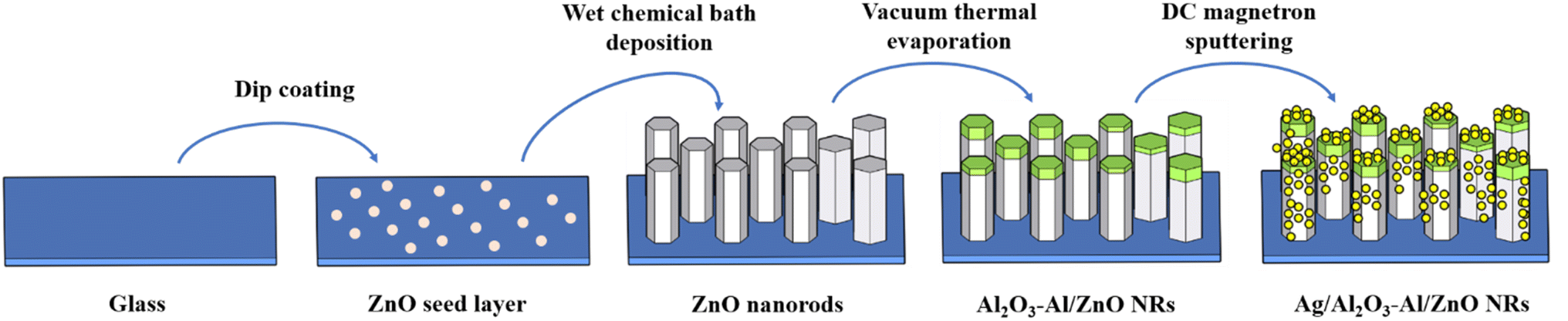
Fig. 1 presents the schematic illustration of fabricating Ag/Al2O3–Al/ZnO NRs SERS substrate. The ZnO NRs are developed on glass, then covered with Al2O3–Al thin film and decorated with Ag NPs.
 |
| | Fig. 1 Schematic illustration of fabricating Ag/Al2O3–Al/ZnO NRs SERS substrate – ZnO NRs is developed on glass, then covered with Al2O3–Al thin film and decorated with Ag NPs. | |
2.1.1 Preparation of ZnO NRs. Firstly, ZnO seed layer is synthesized by the sol–gel method. ZnO solution is prepared by mixing ethylene glycol ethyl ether (2-methoxylethanol) and monoethanolamine (MEA). The solution is stirred for 30 minutes at room temperature. Then zinc nitrate dehydrates (Zn (NO3)2·2H2O) are added to the above mixture and kept stirred for 15 minutes. This solution is continuously stirred at 60 °C for 30 minutes. Then ZnO seed layers are covered on the glass slides by the dip coating method. The dip-coating is carried out at the rate of 4 cm min−1 after embedding the glass slide in ZnO solution for 10 minutes. After each dip process, films are dried at 250 °C in the air for 30 minutes. Secondly, ZnO NRs are grown on the seed layer by chemical bath process with the solutions of 0.1 M hexamethylenetetramine (Zn (NO3)2·6H2O) and 0.1 M zinc nitrate hexahydrate (C6H12N4). After mixing the two solutions in a volume ratio of 1![[thin space (1/6-em)]](https://www.rsc.org/images/entities/char_2009.gif) :1, the mixed solution is magnetically stirred for 30 min. The ZnO seed sample is immersed in this solution mixture, slowly heated to 90 °C, and then kept at a constant temperature. After 4 hours, stop heating and let the system return to room temperature. The ZnO NRs sample is washed twice with distilled water and dried in the air environment.
:1, the mixed solution is magnetically stirred for 30 min. The ZnO seed sample is immersed in this solution mixture, slowly heated to 90 °C, and then kept at a constant temperature. After 4 hours, stop heating and let the system return to room temperature. The ZnO NRs sample is washed twice with distilled water and dried in the air environment.
2.1.2 Fabrication of Al2O3–Al layer by the vacuum thermal evaporation process. Al thin film is deposited on the ZnO NRs substrate by the vacuum thermal evaporation method. 99.9% purity aluminum foil after surface treatment is cut into wires and put in the tungsten boat. The distance between the substrate holder and the tungsten boat is 5 cm. The base pressure of the vacuum chamber is 2 × 10⁻⁵ Torr. The current supply is 30 A. And then, the Al thin film is annealed at 300 °C for 2 hours in the air environment to modify the Al2O3–Al/ZnO NRs substrate. The amount of Al wire is changed at 0.3 mg, 1.0 mg, and 1.7 mg to find the optimal thermal evaporation conditions for testing the SERS signals with the R6G reagent.
2.1.3 Synthesis of SERS substrate by Ag sputtering. The Ag NPs are decorated on the Al2O3–Al/ZnO NRs by the DC magnetron sputtering method. The purity of the Ag target is 99.99%. The base pressure is 2.87 × 10⁻⁶ Torr and the working gas (Ar) is 6.19 × 10⁻³ Torr. During all the sputtering processes, the power and distance between the target and substrates are kept at 9 W and 7 cm, respectively. The sputtering time is changed to 5, 10, 15, and 20 seconds, respectively, and annealed at 200 °C for 15 min to control the size of Ag NPs and the distance between them.
2.2 Characterization
The structure, surface morphology, optical properties, and elements in the SERS substrates are characterized by XRD (Brucker D2 Phaser), Raman spectroscopy (Horiba XploRa PLUS), FE-SEM (Hitachi S4800), UV-vis (PB-10, power 200 W), reflectance spectroscopy (Shimadzu UV probe 2550), and energy dispersion X-ray spectroscopy (EDS) mapping (Horiba H-7593).
2.3 Raman measurements
SERS substrates 1 × 1 cm2 are prepared for Raman measurements. Raman signals are recorded by the Horiba XploRa PLUS Raman system with a 532 nm laser at the power of 1.5 mW. The laser spot area focused on the sample is 1 μm in diameter. The acquisition time is 1 s, the accumulation is 2, and the filtered laser is 1%. The signal is recorded and proceeded. R6G reagent solutions with different concentrations (10−5 to 10−11 M) are used as the probe molecules. The best sensitive SERS substrates are used to detect MNZ as shown in Fig. 2.
 |
| | Fig. 2 Schematic illustration of SERS analysis for using Ag/Al2O3–Al/ZnO NRs substrate to detect R6G and MNZ. | |
3 Results and discussion
3.1 Crystal structure, surface morphology, and optical property of a-Al2O3–Al/ZnO nanorods
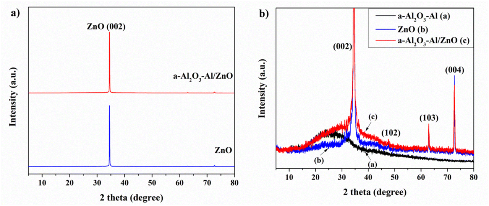
3.1.1 Crystal structure. To investigate the properties of a-Al2O3–Al/ZnO nanorods, an aluminum layer is fabricated by the vacuum thermal evaporation method from the pure aluminum foil of 1.0 mg and after annealing in the air environment at 300 °C for 2 hours. Fig. 3(a) reveals the XRD pattern of the ZnO NRs structure before and after being covered with an aluminum thin layer. Both structures present a similarity in appearance with the sharp and highest intensity peak in the (002) plane at the 2θ of 34.4°. Fig. 3(b) shows the appearance of weak intensities of (102), (103), and (004) planes at the 2θ of 47.5°, 62.9°, and 72.3° of ZnO NRs (JCPDS File No. 36-1451_ZnO). These samples possess hexagonal wurtzite structures orientating highly along the c-axis direction with good crystal quality. In addition, the XRD pattern in Fig. 3(b) displays the presence of the amorphous alumina phase after Al thin film is deposited on a glass substrate post-anneals in the air environment at 300 °C for 2 hours. This result consists of that of Gangwar et al.32 It can be explained that even at room temperature, the aluminum surface always appears as an amorphous alumina (a-Al2O3) layer due to its interface energy being lower than that of crystalline states.33 Annealing aluminum at 300 °C for 2 hours in the air environment accelerates the formation of amorphous alumina (a-Al2O3).
 |
| | Fig. 3 (a) The XRD pattern of the ZnO NRs structure before and after being covered with aluminum supper thin film. (b) Comparison between the ZnO NRs structure before and after being covered with aluminum supper thin film and the aluminum on the glass substrate. | |
Thomas et al. reported in their research that the surface of the oxidized aluminum film contains Al3+ cation in the tetrahedral and octahedral interstices of disordered cubic packing networks of γ-Al2O3. The tetrahedral AlO4 and octahedral AlO6 groups exist in two common isolated and condensed states. The vibrational frequency of the Al–O bond which provides the structural information of the oxidized aluminum film depends on the coordination number of the Al3+ cation.34 In this study, the structural Raman spectrum of annealing aluminum thin film in Fig. 4(a) shows that the 790 cm−1 peak is related to AlO4 tetrahedra (condensed and isolated), the strong peak at 567 cm−1 corresponds to condensed AlO6 octahedra, the weak band of 418–488 cm−1 according to isolated AlO6 octahedra. The band at 246, 303, and 331 cm−1 are assigned to the bending vibration of AlO4 and AlO6. The appearance of AlO4 vibration in the Raman spectrum illustrates the amorphous property of the oxidized aluminum surface. Annealing the aluminum at 300 °C for 2 hours enhances the oxidation surface and structure due to the higher intensity of condensed AlO6 octahedra at the 567 cm−1 peak.34
 |
| | Fig. 4 The Raman structure spectra of (a) the annealing aluminum thin film at 300 °C for 2 hours in the air environment and (b) the ZnO NRs before and after being covered with annealing aluminum thin film. | |
Fig. 4(b) presents the Raman structure spectra of the ZnO NRs before and after being covered with an annealing aluminum thin film. In both cases, the characteristic Raman peaks of the ZnO structure appear. The low peaks at 371 cm−1 and 567 cm−1 correspond to A1 (Transversal Optical – TO) mode and A1 (Longitudinal Optical – LO) mode which are the lattice vibrations when atoms move parallel to the c-axis. The very high peaks at 94 cm−1 and 432 cm−1 assign to E2L and E2H modes. Where the low-frequency mode (E2L) is associated with the heavy Zn sublattice and the high-frequency mode (E2H) involves only oxygen atoms. The result shows the ZnO NRs sample crystalizing well in a hexagonal wurtzite structure and almost remains unchanged after being coated with the annealing aluminum film. In the spectrum of a-Al2O3–Al/ZnO, the 476 cm−1 peak relates to the isolated AlO6 octahedra of a-Al2O3–Al. The other peaks cannot be seen due to overlap with those of ZnO and the low concentration of oxidized aluminum thin film.
3.1.2 Surface morphology. The surface morphology of the substrate plays an important role in scattering the incident light. The higher the effective surface area, the better the performance of the SERS substrate3–5 The FE-SEM image in Fig. 5(a) illustrates the hexagonal morphology of ZnO NRs with a diameter in the range of 100–150 nm. Fig. 5(b) shows the cross-section image of the aluminum thin film deposited on glass by the vacuum thermal evaporation method. After annealing at 300 °C for 2 hours in the air environment, the amorphous aluminum layer with a thickness of 120 nm is formed on the Al thin film. The FE-SEM image of the a-Al2O3–Al/ZnO sample in Fig. 5(c) exhibits almost the high effective surface area as ZnO. Fig. 5(d) presents the cross-section image of a-Al2O3–Al/ZnO nanorods. The ZnO seeds layer coated on glass by simple technique (dip-coating) plays an important role in growing ZnO NRs. It assists ZnO NRs in growing perpendicular to the substrate in chemical bath immersion. Fig. 5(d) shows that ZnO NRs on the seeds layer are well aligned and uniform, growing on the c-axis [0 0 2] perpendicular to the substrate. The effective surface area of ZnO nanorods after being coated by the a-Al2O3–Al layer will not decrease much because this aluminum film is thin. There is still a good gap between the ZnO NRs which creates a highly effective surface area and increases the scattering of incident light. Thus, a-Al2O3–Al/ZnO NRs structure can be a good candidate for SERS substrate.
 |
| | Fig. 5 (a) The FE-SEM image of ZnO nanorods, (b) the cross-section image of oxidized aluminum thin film (a-Al2O3–Al) annealed at 300 °C for 2 hours on glass, (c) the FE-SEM image of a-Al2O3–Al/ZnO nanorods, and (d) the cross-section image of a-Al2O3–Al/ZnO nanorods. | |
3.1.3 Optical property. The UV-vis absorption spectra of ZnO NRs and a-Al2O3–Al/ZnO NRs in Fig. 6(a) show that ZnO NRs is a direct optical band gap semiconductor with an absorption edge of 385 nm and it remains unchanged after being coated with an oxidized aluminum thin film. The optical band gap (Eg) of these semiconductor materials is equal to 3.25 eV which is determined by linear extrapolation in the inset of Fig. 6(a) based on the Tauc relation, (αhυ)2 = B(hυ − Eg), where B, Eg, hυ, and α are constant, the optical band gap energy, the photon energy, and the absorption coefficient, respectively. In addition, Fig. 6(a) indicates the absorbance of a-Al2O3–Al/ZnO NRs substrates is higher than that of pure ZnO NRs substrate due to the thicker layer after being coated with an oxidized aluminum thin film.
 |
| | Fig. 6 (a) The UV-vis absorption spectra of ZnO NRs and a-Al2O3–Al/ZnO NRs, and (b) the reflectance spectra of ZnO NRs and a-Al2O3–Al/ZnO NRs. | |
The reflectance spectra of ZnO NRs and a-Al2O3–Al/ZnO NRs substrates are compared to evaluate their optical performance. Fig. 6(b) shows the reflectance of ZnO NRs substrate is about 10.5% at the wavelength of 500 nm and only 5% at 800 nm. However, that of a-Al2O3–Al/ZnO NRs substrates decreases to 9.5% and 4% at 500 nm and 800 nm, respectively. This may be explained that the surface of ZnO NRs becomes rougher due to the shrinkage of the a-Al2O3–Al layer on ZnO NRs. The result indicates that the a-Al2O3–Al/ZnO NRs substrates can trap the incident light more effectively than the ZnO NRs substrate for larger scattering and absorbance.
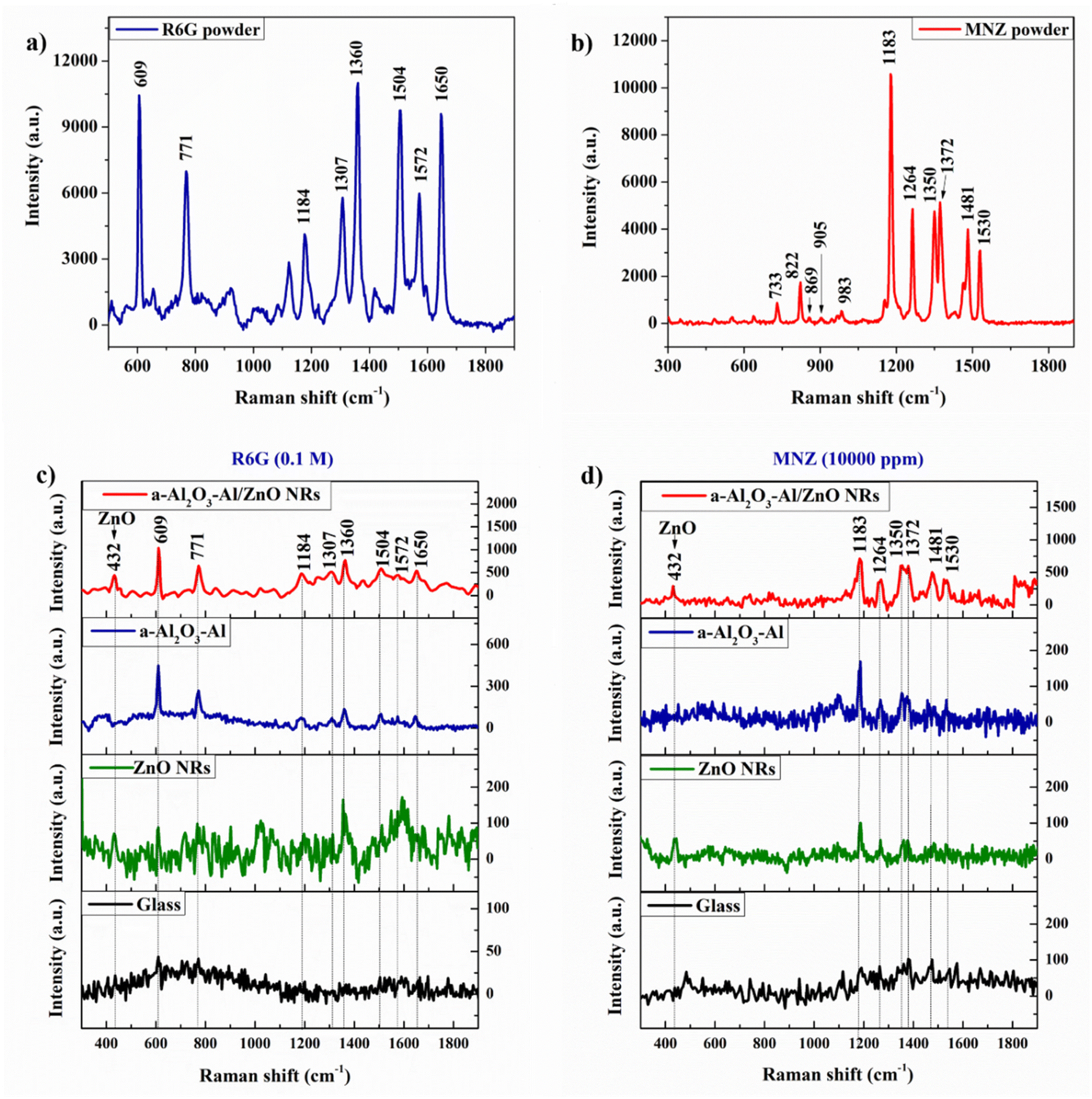
3.1.4 The role of ZnO nanorods and a-Al2O3–Al thin film in enhancing the Raman signal of reagent molecules. Firstly, we consider the behavior of semiconductor substrates without Ag NPs on the SERS signal. The R6G reagent is used to investigate the role of the semiconductor in enhancing the SERS signal because it is a low-cost dye and easy detection of the Raman signal. And then, the best substrate is used to detect MNZ. The Raman spectrum of the R6G and MNZ powders recorded is shown in Fig. 7(a and b) which is used to compare to that of their solution. Fig. 7(c and d) presents the Raman signal of R6G (0.1 M) and MNZ (10000 ppm) solutions which are dropped individually on the various substrates of bare glass, ZnO NRs, a-Al2O3–Al thin film, and a-Al2O3–Al/ZnO NRs with the same amount of 50 μL. The result in Fig. 7 illustrates that bare glass substrate cannot detect both R6G and MNZ, but the other semiconductor substrates can recognize these organic molecules. The 432 cm−1 peak of the ZnO structure appears in both Raman spectra of R6G and MNZ absorbed on the ZnO NRs and a-Al2O3–Al/ZnO NRs substrates.
 |
| | Fig. 7 The Raman spectrum of (a) R6G powder, (b) MNZ powder, the SERS spectra of (c) R6G solution at 10−5 M, and (d) MNZ solution at 104 ppm that absorbed onto the bare glass, ZnO NRs, a-Al2O3–Al thin film, and a-Al2O3–Al/ZnO NRs substrates. | |
For the R6G reagent, the experimental Raman peaks which are assigned to the characteristic vibration bands of the R6G molecule shown in Table 1 coincide with the DFT and powder Raman spectrum. The Raman signal intensity and the number of peaks of organic molecules increase from ZnO NRs to a-Al2O3–Al thin film. The a-Al2O3–Al/ZnO NRs substrate has the highest intensity of Raman signal and appears most of the peaks of R6G at solution 0.1 M. The 610 cm−1 peak of the solution possesses the highest intensity in all spectra and is used to investigate the sensitivity of the SERS substrates. The result in Table 1 shows that compare to the bare glass, the intensity of 610 cm−1 peak on ZnO NRs, a-Al2O3–Al thin film, and a-Al2O3–Al/ZnO NRs substrates is higher than 2, 10.2, and 23.6 times, respectively. In the case of MNZ, a similar result in Table 2 shows that a-Al2O3–Al/ZnO NRs substrate can enhance the Raman signal of MNZ better than the other substrates and detect most Raman peaks of MNZ powder. The intensity of the chosen peak at 1184 cm−1 on ZnO NRs, a-Al2O3–Al thin film, and a-Al2O3–Al/ZnO NRs substrates is 1.2, 2.2, and 9.9 times compared to bare glass, corresponding.
Table 1 The DFT and experimental Raman signal of R6G
| DFT35 |
R6G powder |
Experimental (R6G 0.1 M) |
Vibrational assignment |
| Glass |
ZnO NRS |
a-Al2O3–Al |
a-Al2O3–Al/ZnO NRs |
| ν (cm−1) |
ν (cm−1) |
ν (cm−1) |
Raman int. |
ν (cm−1) |
Raman int. |
ν (cm−1) |
Raman int. |
ν (cm−1) |
Raman int. |
| 610 |
609 |
610 |
43.8 |
610 |
87.3 |
610 |
446.8 |
610 |
1031.7 |
C–C–C ring in-plane |
| 771 |
771 |
772 |
41.6 |
772 |
98.0 |
772 |
268.2 |
772 |
643.8 |
C–H out-plane bending |
| 1192 |
1184 |
|
|
1185 |
69.9 |
1185 |
74.34 |
1185 |
475.0 |
C–H in-plane bending |
| 1307 |
1307 |
|
|
|
|
1309 |
71.1 |
1306 |
514.4 |
C–O–C stretching |
| 1360 |
1360 |
|
|
1363 |
164.7 |
1360 |
136.7 |
1363 |
766.0 |
C–O–C stretching |
| 1505 |
1504 |
|
|
1508 |
94 |
1508 |
101.7 |
1508 |
587.0 |
C–O–C stretching |
| 1577 |
1572 |
|
|
|
|
1575 |
82.9 |
1575 |
475.5 |
C–C stretching of the aromatic ring |
| 1652 |
1650 |
|
|
|
|
1646 |
84.4 |
1650 |
535.7 |
C–O–C stretching |
Table 2 The DFT and experimental Raman signal of MNZ
| MNZ powder |
Experimental (MNZ 10000 ppm) |
Vibrational assignment36,37 |
| Glass |
ZnO NRS |
a-Al2O3–Al |
a-Al2O3–Al/ZnO NRs |
| ν (cm−1) |
ν (cm−1) |
Raman int. |
ν (cm−1) |
Raman int. |
ν (cm−1) |
Raman int. |
ν (cm−1) |
Raman int. |
| 730 |
|
|
|
|
|
|
|
|
CH2 rocking |
| 822 |
|
|
|
|
|
|
|
|
Ring breathing |
| 869 |
|
|
|
|
|
|
|
|
CH3 rocking |
| 905 |
|
|
|
|
|
|
|
|
CH2 out of plane bending |
| 983 |
|
|
|
|
|
|
|
|
O–H bending |
| 1183 |
1184 |
71.7 |
1186 |
100.2 |
1185 |
158.6 |
1184 |
710.5 |
C–H out of a plane |
| 1264 |
1263 |
82.4 |
1267 |
53.2 |
1267 |
62.2 |
1270 |
389.0 |
C–N stretching |
| 1350 |
1349 |
72.0 |
|
|
1353 |
80.6 |
1349 |
602.5 |
C–C or CH2 stretching |
| 1372 |
1379 |
102.9 |
|
|
1375 |
71.8 |
1379 |
599.9 |
C–N stretching (aromatic) |
| 1481 |
1475 |
100.8 |
1482 |
44.3 |
1481 |
42.9 |
1475 |
520.6 |
CH2 scissoring |
| 1530 |
1534 |
59.5 |
1530 |
41.1 |
1532 |
61.9 |
1534 |
478.7 |
C![[double bond, length as m-dash]](https://www.rsc.org/images/entities/char_e001.gif) C vibration C vibration |
These results are explained by the contribution of the vertical ZnO NRs surface morphology and the localized surface plasmon resonance (LSPR) of Al in the EM and the support of charge transfer between the semiconductor and organic molecules in the CE. The Raman signal of both R6G and MNZ solution absorbed on ZnO NRs substrate is higher than on glass due to (1) the high effective surface area of one-dimensional structures of vertical ZnO nanorods increases the scattering of the incident light, and (2) the edges of the ZnO NRs hexagonal structure increase the electric field. The LSPR of Al nanostructure in a-Al2O3–Al thin film is the main reason for the enhanced Raman signal of these organics compared to ZnO NRs and glass substrates. Indeed, some metals (Au, Ag, and Al) can be considered free-electron systems because the electronic and optical properties of these metals are determined by the conduction electrons. Due to the electric field of the incident light, the free surface electrons of the metals oscillate collectively. When the frequency of the collective oscillation is equal to that of the incident photon, resonance occurs resulting in the metal strongly absorbing and scattering incident light. This property of metal namely localized surface plasmon resonance (LSPR).3,29 In addition to the Raman signal of organics enhanced by the EM, it is also enhanced by the CM when these substances are absorbed on the ZnO NRs and a-Al2O3–Al structure. The role of ZnO NRs and a-Al2O3–Al thin film in the charge transfer is illustrated in Fig. 8. The energy levels of the conduction band edge (ECB) and valence band edge (EVB) of ZnO and Al2O3 are calculated by ECB = −χ + 0.5 × Egand EVB = ECB − Eg, respectively. Where χ is the absolute electronegativity of the semiconductor material in the theoretical calculator, and χ (ZnO) = 5.79 eV,38 χ (Al2O3) = 5.35 eV.39 The optical band gap of ZnO in our experimental measurement is 3.25 eV. Zhendong Guo et al. calculated the band gap of a-Al2O3 to be 6.67 eV based on the use of an atomistic model structure through ab initio molecular dynamics and the HSE function which matches the published experimental values.40 In addition, the surface state energy level (Ess) of semiconductors contributed to the CT of SERS which is indicated in the published papers.12,41 The surface defects such as surface oxygen vacancy defects in ZnO12,41,42 and Al2O3 (ref. 39) produce this Ess. Furthermore, the vertical ZnO nanorod conducts electrons in one dimension significantly increasing the charge transfer in the CT mechanism.
 |
| | Fig. 8 Charge transfer diagram of a-Al2O3–Al/ZnO NRs with (a) R6G reagent and (b) MNZ. | |
Fig. 8(a) shows that the highest occupied molecular orbital (HOMO) and the lowest unoccupied molecular orbital (LUMO) levels of R6G are −5.7 eV and −3.4 eV, respectively.43 The exciting energy of laser 532 nm (2.33 eV) is approximately the LUMO–HOMO bandgap, so electrons from HOMO may get excited to the LUMO level. These hot electrons move to HOMO and emit characteristic vibrations of the R6G molecules. However, the results in Table 1 and Fig. 7(c) show the signal almost is not recorded. The energy of the excited laser may not be strong enough to excite the electrons to the LUMO level. The Raman intensity of R6G increases slightly when the R6G solution is absorbed by the ZnO NRs. It is because the hot electrons are easily transferred to the LUMO level through the Ess and CB levels of ZnO and following the solid arrow lines. In the case of R6G absorption on an a-Al2O3–Al thin film, the hot electrons can move to the LUMO lever in more ways than ZnO, resulting in a better signal. Therefore, the combination of ZnO and a-Al2O3–Al enhances the Raman signal base on the CT. Fig. 8(b) shows a similar scheme of CT for MNZ. Because MNZ molecules' HOMO and LUMO levels are −6.96 eV and −2.35 eV, respectively,28 it takes at least 4.61 eV for electrons to move from the HOMO level to the LUMO level of MNZ. However, with the assistance of structure a-Al2O3–Al/ZnO NRs, hot electrons move easily from HOMO to the LUMO level of MNZ. In addition, the gap between LUMO and HOMO of MNZ is large than that of R6G, the electron cannot transfer to CB of ZnO to move to LUMO. So the a-Al2O3–Al thin film has an important role in the charge transfer of MNZ through the Ess of a-Al2O3 and EF level of Al.
Thus, the a-Al2O3–Al/ZnO NRs substrate possesses the outstanding advantages of the vertical ZnO NRs and a-Al2O3–Al thin film in enhancing the Raman signal by EM and CE. It concludes (1) the high effective surface area of one-dimensional structures of vertical ZnO nanorods increases the scattering of the incident light, (2) the edges of the ZnO NRs hexagonal structure increase the electric field, (3) the vertical ZnO nanorod conducts electrons in one dimension significantly increasing the charge transfer in the CT mechanism, (4) the LSPR of Al nanostructure supports the strongly absorbing and scattering incident light. In CE, the contribution of the Ess levels due to the defects in ZnO and Al2O3 is very important for supporting charge transfer between the semiconductor substrate and organic molecules.
Finally, we consider the efficiency of these semiconductor structures in combination with Ag nanoparticles. The SERS substrates of Ag/glass, Ag/ZnO NRs, Ag/a-Al2O3–Al thin film, and Ag/a-Al2O3–Al/ZnO NRs are coated with Ag NPs for the same 10 s sputtering time. The recorded SERS signals of R6G (10−5 M) and MNZ (100 ppm) absorbed on these SERS substrates are shown in Fig. 9. The four SERS substrates detect the R6G and MNZ solution at low concentrations with the well-characterized peaks and high intensity in the Raman spectrum. This result shows the huge role of the LSPR peak of Ag NPs in the enhancement of the SERS signal.3 Table 3 presents the Raman intensity of R6G (0.1 M), MNZ (104 ppm) absorbed on the glass, ZnO NRs, a-Al2O3–Al thin film, a-Al2O3–Al/ZnO NRs, and that of R6G (10−5 M), MNZ (100 ppm) absorbed on the SERS substrates of Ag/glass, Ag/ZnO NRs, Ag/a-Al2O3–Al thin film, Ag/a-Al2O3–Al/ZnO NRs. The ratio of signal/noise (S/N) increases in order from the substrates of glass, ZnO NRs, a-Al2O3–Al thin film, and a-Al2O3–Al/ZnO NRs both in combination with Ag and without Ag. The ZnO NRs structure has a highly effective surface area with the vertical nanorods to which many noble metal nanoparticles can be attached to create a “hot-spot” density that increases the electric field. And, the Ess level of ZnO support in charge transfer. These advantages of ZnO NRs make the Ag/ZnO NRs sample sensitive in enhancing the Raman signal, especially in the case of R6G. In addition to possessing the good characteristics of ZnO NRs structure, the Ag/a-Al2O3–Al/ZnO NRs substrate also contains many beneficial properties of Ag/a-Al2O3–Al layer such as the support of the LSPR of Al nanostructure in EM and the Ess level of a-Al2O3 in the CM. Since then, the SERS substrate of Ag/a-Al2O3–Al/ZnO NRs is more effective than Ag/glass, Ag/ZnO NRs, and Ag/a-Al2O3–Al thin film in enhancing the SERS signal, especially in case of MNZ. Therefore, the Ag/a-Al2O3–Al/ZnO NRs substrate could potentially be used as a SERS substrate to detect MNZ at a low concentration.
 |
| | Fig. 9 SERS spectra of (a) R6G solution (10−5 M), and (b) MNZ solution (100 ppm) absorbed on the Ag/glass, Ag/ZnO NRs, Ag/a-Al2O3–Al thin film, and Ag/a-Al2O3–Al/ZnO NRs substrates. | |
Table 3 The Raman intensity of rhodamine 6G at 609 cm−1 peak with the concentration of 0.1 M on the glass, ZnO NRs, a-Al2O3–Al thin film, a-Al2O3–Al/ZnO NRs, and 10−7 M on Ag/glass, Ag/ZnO NRs, Ag/a-Al2O3–Al thin film, Ag/a-Al2O3–Al/ZnO NRs substrates. The Raman intensity of metronidazole at 1183 cm−1 peak with the concentration of 104 ppm on the glass, ZnO NRs, a-Al2O3–Al thin film, a-Al2O3–Al/ZnO NRs, and 100 ppm on Ag/glass, Ag/ZnO NRs, Ag/a-Al2O3–Al thin film, Ag/a-Al2O3–Al/ZnO NRs substrates
| Substrate |
Rhodamine 6G (R6G) |
Metronidazole (MNZ) |
| Raman intensity at 609 cm−1 peak |
S/N |
Raman intensity at 1183 cm−1 peak |
S/N |
| Glass |
43.8 |
1 |
71.7 |
1 |
| ZnO NRs |
87.3 |
2 |
100.2 |
1.4 |
| a-Al2O3–Al thin film |
446.8 |
10.2 |
158.6 |
2.2 |
| a-Al2O3–Al/ZnO NRs |
1031.7 |
23.6 |
710.5 |
9.9 |
| Ag/glass |
1199.3 |
27.4 |
285.5 |
4 |
| Ag/ZnO NRs |
1772.6 |
40.5 |
573.4 |
8 |
| Ag/a-Al2O3–Al thin film |
2029.1 |
46.3 |
750.6 |
10.5 |
| Ag/a-Al2O3–Al/ZnO NRs |
2975.9 |
67.9 |
3308.2 |
46.1 |
3.2 Characteristics of Ag/a-Al2O3–Al/ZnO NRs substrates
3.2.1 Role of Ag nanoparticles at various sputtering times on the SERS signal. In this section, we investigate the influence of the “hot spots” distribution of Ag nanoparticles on the performance of the SERS substrate. The size and distribution of Ag NPs which are deposited on a-Al2O3–Al/ZnO NRs by sputtering magnetron DC method at various sputtering times of 5, 10, 15, and 20 s are shown by the FE-SEM image in Fig. 10. The thickness of the Ag thin film greatly affects the size and distribution of Ag NPs formed under the same annealing condition at 200 °C for 15 min. The Ag NPs at 5 s are about 5 nm in size and sparsely distribute on the sample surface (Fig. 10(a)). At 10 s, the Ag NPs are very similar in average diameter of about 20 nm and uniformly distribute throughout the a-Al2O3–Al/ZnO NRs surface with a distance between them of about 20 nm. The FE-SEM image in Fig. 10(b) reveals a high density of “hot spots” Ag NPs which plays an important role in enhancing the SERS signal intensity. When the sputtering time increases to 15 s, Fig. 10(c) shows a significant difference in the size of Ag NPs ranging from 5–20 nm and densely distributed on the nanorods. The nano-gap of Ag NPs decreases clearly to about 1–2 nm. This gap significantly reduces at the sputtering time of 20 s when the Ag layer becomes thicker. From Fig. 10(d) it is possible to observe some Ag nanoparticles with a size of less than 5 nm located on top of other silver nanoclusters.
 |
| | Fig. 10 The FE-SEM images of Ag/a-Al2O3–Al/ZnO NRs SERS substrates with various sputtering times of Ag at (a) 5 s, (b) 10 s, (c) 15 s, and (d) 20 s. | |
The UV-vis absorption spectra are utilized to investigate the surface plasmon resonance of Ag NPs. In the case of the SERS material, the noble metal nanoparticles have a very important contribution to enhancing the Raman signal of reagent molecules due to its LSPR in the visible band of the UV-vis absorption spectroscopy. The amplitude of the enhanced incident light is stronger as the absorption intensity of the LSPR peak is higher, which depends on the shape, size, and internal distance between the metal nanoparticles.4 Fig. 11(a) shows the UV-vis absorption spectra of Ag NPs deposited on the a-Al2O3–Al/ZnO NRs substrates at different sputtering times of 5–20 s. The sharp absorption edge of a-Al2O3–Al/ZnO NRs material remains unchanged at 385 nm in all samples while the LSPR peak intensity of Ag NPs in these samples is remarkably different. The Ag/a-Al2O3–Al/ZnO NRs substrate at 10 s possesses the highest LSPR peak due to the optimal size and distribution of Ag NPs at 10 s as analyzed above. Fig. 11(b) displays the SERS spectra of R6G solution at 10−5 M absorbed on the Ag/a-Al2O3–Al/ZnO NRs SERS substrates with various sputtering times of Ag at 5–20 s. The result illustrates that the characteristic Raman peaks of R6G absorbed on these four SERS substrates are the same as that of R6G powder (Fig. 7(a)). This may be because the presence of Ag nanoparticles on the surface of the SERS substrate enhances the Raman signal due to the good adsorption of organic molecules and the localized surface plasmon resonance of the SERS substrates. Fig. 11(b) also presents the highest SERS signal intensity of the 10 s substrate compared to the others. There is a close relationship between the SERS signal intensity and the LSPR peak intensity of Ag NPs caused by their size, shape, and distribution on the SERS substrate surface. Thus, the substrate with the optimal Ag NPs 10 s is selected to investigate in the next stage.
 |
| | Fig. 11 (a) The UV-vis absorption spectra of Ag/a-Al2O3–Al/ZnO NRs substrates with various sputtering times of Ag at 5–20 s, (b) the SERS signals of R6G solution at 10−5 M are absorbed on the Ag/a-Al2O3–Al/ZnO NRs SERS substrates with various sputtering times of Ag at 5–20 s. | |
3.2.2 Contribution of the thickness of Al film on the sensitivity of Ag/a-Al2O3–Al/ZnO NRs SERS substrate. The Al pieces with different masses are coated on the ZnO NRs by vacuum thermal evaporation method to investigate the effect of the Al film thickness on the sensitivity of Ag/a-Al2O3–Al/ZnO NRs SERS substrate. Fig. 12(a–c) reveals the FE-SEM image of a-Al2O3–Al/ZnO NRs with various thicknesses of Al at 0.3, 1.0, and 1.7 mg. The surface morphology of ZnO NRs in Fig. 12(a) is almost unchanged after being coated by an Al thin film of 0.3 mg which would have been shrunk and changed into a very thin film of a-Al2O3 under the annealing at 300 °C for 2 h in the air environment. The absence of Al thin film can affect the efficiency of charge transfer between organic molecules and SERS substrate. The 1.0 mg Al thin film which is changed to the a-Al2O3–Al thin film with an a-Al2O3 thickness of 120 nm and Al thickness of 180 nm after annealing is shown in Fig. 6(b). These Al and a-Al2O3 layers together support the charge transfer process and have an appropriate thickness so as not to reduce the high effective surface area of ZnO as shown in Fig. 12(b). This a-Al2O3–Al layer is very useful in increasing the surface roughness, reducing the reflection, and thus increasing the scattering of incident radiation as mentioned above. The Al film at 1.7 mg is so thick that after annealing it forms a layer of a-Al2O3–Al that covers the space between the ZnO NRs, binding these nanorods together, and making the effective surface area of the sample greatly reduced as shown in Fig. 12(c). The SERS signals of R6G solution at 10−5 M absorbed on the Ag (10 s)/a-Al2O3–Al/ZnO NRs SERS substrates with various thicknesses of Al at 0.3, 1.0, and 1.7 mg s are shown in Fig. 12(d). Due to the disadvantage of reduced effective surface area, the SERS signal intensity of R6G 10−5 M absorbed SERS substrate of 1.7 mg Al is the lowest in the three SERS substrates. This result shows that the optimal surface for the support in CT of the a-Al2O3–Al/ZnO NRs platform is 1.0 mg of Al.
 |
| | Fig. 12 The FE-SEM image of a-Al2O3–Al/ZnO NRs NRs with various thicknesses of Al at (a) 0.3, (b) 1.0, and (c) 1.7 mg, and (d) the SERS signals of R6G solution at 10−5 M are absorbed on the Ag (10 s)/a-Al2O3–Al/ZnO NRs SERS substrates with various thicknesses of Al at 0.3, 1.0, and 1.7 mg. | |
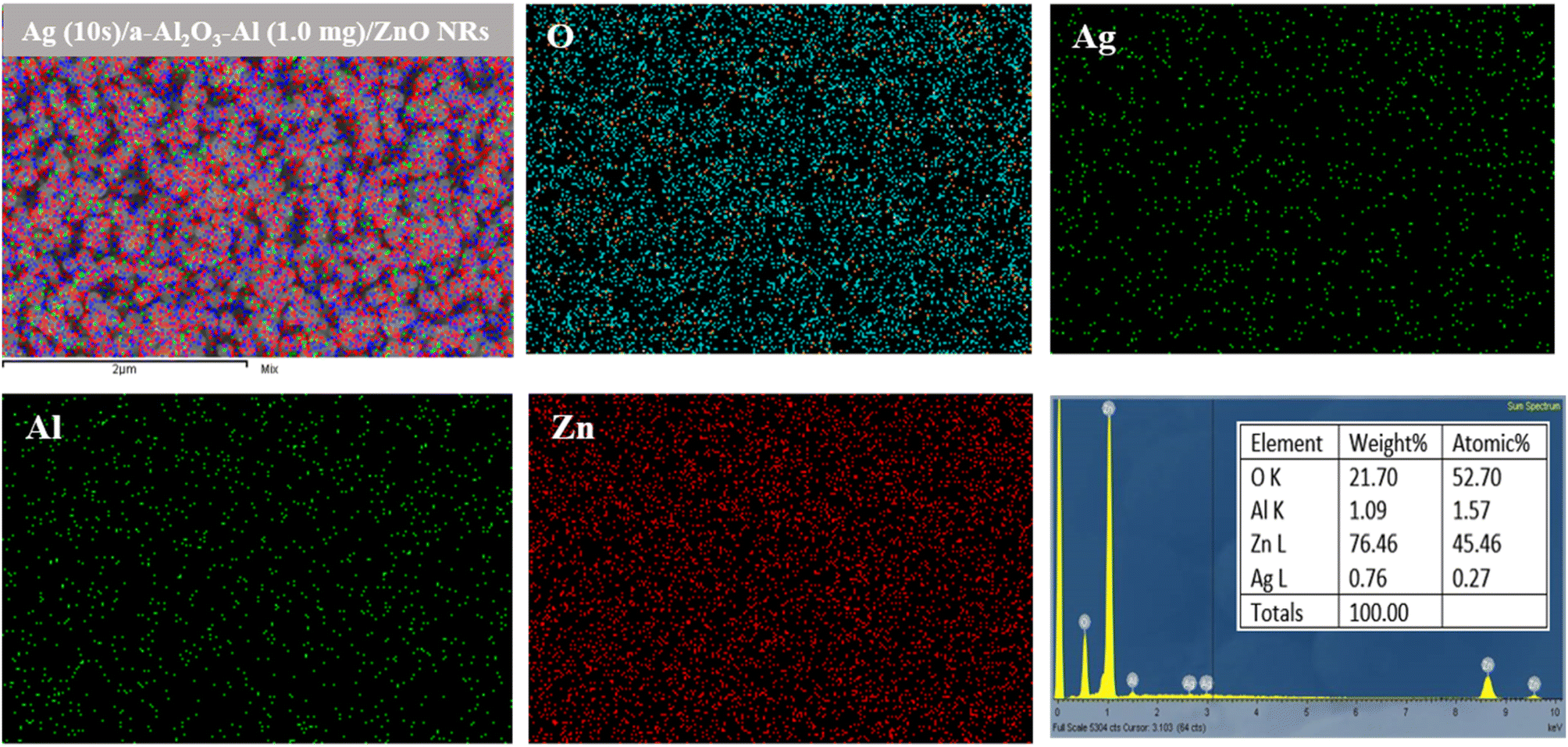
Fig. 13 shows the EDS analysis of the Ag (10 s)/a-Al2O3–Al (1.0 mg)/ZnO NRs SERS substrate. The EDS mapping in Fig. 13(a–e) shows that the elements of Ag, Al, and O distribute homogeneously on ZnO nanorods. The result in Fig. 13(f) reveals the presence of Zn, O, Al, and Ag elements that correspond to 45.46%, 52.70%, 1.57%, and 0.27% atomic, respectively.
 |
| | Fig. 13 The EDS analysis of Ag (10 s)/a-Al2O3–Al (1.0 mg)/ZnO NRs SERS substrate. | |
Thus, the Ag/a-Al2O3–Al/ZnO NRs sample with Al-1.0 mg and Ag-10 s possess the optimal characteristics in terms of the structure, optical properties, and surface morphology, so it should be selected as a SERS substrate to detect the MNZ.
3.3 Detection of metronidazole by using the Ag (10 s)/a-Al2O3–Al (1.0 mg)/ZnO NRs SERS substrate
Specificity is one of the method validation parameters. Specificity is defined by ICH guideline Q2 (R1) that specificity can be shown by demonstrating that the identification and/or quantitation of an analyte is not impacted by the presence of other substances (e.g., impurities, degradation products, related substances, matrix, or other components present in the operating environment).44 The specificity of the method in this study is based on the Raman signal of the MeOH solvent and organic molecules absorbed on the SERS substrate. Fig. 14 shows that the 432 cm−1 peak of the ZnO structure appears in the three Raman spectra. Apart from this characteristic peak of the SERS substrate, no signal of MeOH is detected when it is absorbed on the SERS signal. Therefore, the Raman spectra of R6G and MNZ are their specific SERS spectra.
 |
| | Fig. 14 The Raman signal of the MeOH solvent, R6G (10−5 M), and MNZ (104 ppm) solutions absorbed on the Ag (10 s)/a-Al2O3–Al (1.0 mg)/ZnO NRs SERS substrate. | |
The SERS enhancement factor (EF) is used to estimate the sensitivity of a SERS substrate and calculated by the formulation of EF = (ISERS/NSERS) × (Nbare/Ibare), where Ibare and ISERS correspond to the normal Raman intensity and SERS of organic molecules. Nbare = Cbare × V is the average number of absorbed molecules in the scattering volume, V, for the Raman (non-SERS) measurement, and NSERS = CSERS × V is the average number of molecules in the same scattering volume for the SERS experiments.3 The limit of detection (LOD) is defined as the lowest concentration of an analyte in a sample that can be consistently detected with a stated probability (typically at 95% certainty).45
In this study, R6G reagent solution at a concentration from 10−5 to 10−11 M and MNZ standard solution at a concentration between 10 and 0.01 ppm are prepared to define the EF and LOD of the SERS substrate. The result in Fig. 15 illustrates that the signal intensity increases with the increase in the concentration of both R6G and MNZ solution. The 432 cm−1 peak of the ZnO structure is presented in the spectra which shows the good crystallinity quality of the SERS substrate. The characteristic peaks of R6G and MNZ molecules are recorded in all solution samples of various concentrations. The characteristic peaks of R6G and MNZ molecules on the SERS substrate are still present clearly at very low concentrations of 10−11 M and 0.01 ppm respectively but are not observed on the bare glass substrate at very high concentrations of R6G 0.1 M and MNZ 104 ppm (Fig. 16). This again demonstrates the great role of the SERS substrate in enhancing the Raman signal of organic molecules, especially at very low concentrations. The signal intensity of R6G at peak 609 cm−1 and MNZ at peak 1183 cm−1 are the highest among all the solution samples selected for EF calculation. The LOD and EF of R6G absorbed on the Ag (10 s)/a-Al2O3–Al (1.0 mg)/ZnO NRs SERS substrate calculated from Fig. 16(a and b) respectively 10−11 M and 1.85 × 10¹⁰. These for MNZ are corresponding to 0.01 ppm and 2.2 × 10⁶ (Fig. 16(c and d)). To explain the high sensitivity of the SERS substrate in the detection of R6G and MNZ at a low concentration, we propose a charge transfer scheme of chemical mechanic (CM) in Fig. 17. Besides the support of the a-Al2O3–Al (1.0 mg)/ZnO NRs semiconductor substrate, the Ag NPs with Fermi energy level of −4.7 eV46 create hot electrons due to the excitation of laser 532 nm which allows the charge to transfer easily from the HOMO level of the organic molecules to its EF level and the semiconductor substrate to the LUMO level.
 |
| | Fig. 15 The Raman signal of (a) R6G reagent solutions, and (b) MNZ standard solutions absorbed on the SERS substrate. | |
 |
| | Fig. 16 The Raman signal of R6G reagent solution absorbed on (a) the SERS substrate, (b) the bare glass substrate, the Raman signal of MNZ standard solution absorbed on (c) the SERS substrate, and (d) the bare glass substrate. | |
 |
| | Fig. 17 Charge transfer diagram of Ag (10 s)/a-Al2O3–Al (1.0 mg)/ZnO NRs SERS substrate with (a) R6G reagent and (b) MNZ. | |
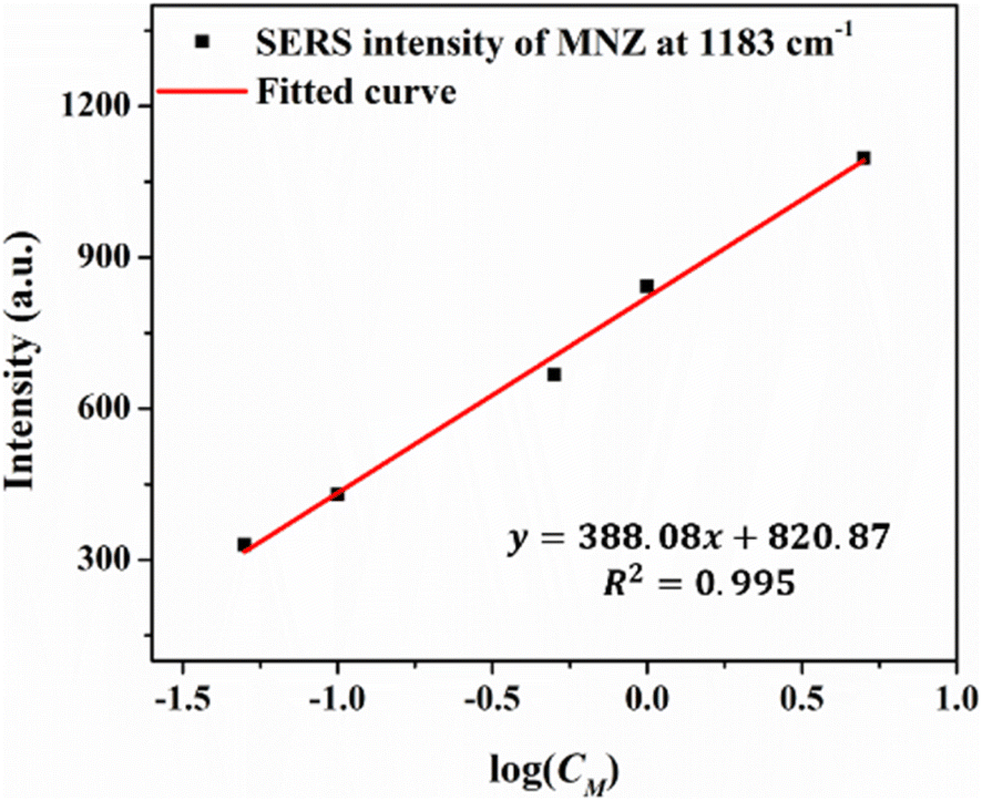
Chunlei Huang et al. provided a substrate based on the hybridization of jellyfish-like zinc oxide microparticles and silver nanoparticles (JF ZnO@Ag) that can detect R6G with an enhancement factor (EF) of 7.58 × 10⁶. Our SERS substrate with EF of 1.85 × 10¹⁰ is much more sensitive than that of the Huang group.9 Caiqin Han et al. prepared the SERS-active silver nanorod (Ag NR) array substrates to detect MNZ with a LOD of 10 μg mL−1 (10 ppm).37 The LOD of the SERS substrate with the combination of multilayer graphene and gold nanoparticles used to detect the MNZ of Sandra Benítez-Martínez et al. is 1.1 mg L−1 (1.1 ppm).47 Compared with the results of these published papers, our highly sensitive SERS substrate detects MNZ with a lower LOD. Table 4 presents the SERS intensity of MNZ at 1183 cm−1 corresponds to the concentrations from 0.01 to 10 ppm. Fig. 18 shows the linear interval between 0.05 and 5 ppm with a very good linear relationship between the 1183 cm−1 peak and the concentration of MNZ. The fitting equation is IMNZ = 388.08 × log(CMNZ) + 820.87, where IMNZ and CMNZ are the SERS intensity at 1183 cm−1 peak and concentration of MNZ solution, respectively. With R2MNZ = 0.995, the SERS method base on the Ag (10 s)/a-Al2O3–Al (1.0 mg)/ZnO NRs substrate is promising for quantitative detection according to ICH guideline Q2(R2) on validation of analytical procedures.44
Table 4 The SERS intensity of MNZ at 1183 cm−1 corresponds to the concentration
| Concentration |
(ppm) |
0.01 |
0.05 |
0.1 |
0.5 |
1 |
5 |
10 |
| SERS intensity at 1183 cm−1 |
(a.u.) |
173.35 |
329.59 |
429.60 |
666.64 |
843.17 |
1096.80 |
2040.03 |
 |
| | Fig. 18 The linear relationship of the peak intensity at 1183 cm−1 as a logarithmic function of MNZ concentrations ranging between 5 ppm and 0.05 ppm. | |
3.4 The spectral reproducibility of the Ag (10 s)/a-Al2O3–Al (1.0 mg)/ZnO NRs SERS substrate
Reproducibility is assessed through an inter-laboratory trial and should be considered in the case of standardization of an analytical procedure.44 In this study, we evaluate the spectral reproducibility of our SERS substrate on the R6G reagent solution with a concentration of 10−7 M on three samples fabricated with the same conditions. We measure six different positions from the center to the outer edge of each sample. The SERS spectra in Fig. 19 show that 18 positions of these three substrates all detect traces of the R6G solution at a low concentration of 10−7 M with all its characteristic peaks. The intensity of the peak at 609 cm−1 in these SERS spectra does not change much, so it is chosen to evaluate the spectral reproducibility of the substrate. The signal intensity at the 609 cm−1 peak and the relative standard deviation (RSD) are shown in Table 5. Guidelines on performance criteria for methods of analysis for the determination of pesticide residues in food and feed according to international food standards indicate that the experimental method is acceptable with the RSD ≤ 20%.48 Our method uses the Ag/a-Al2O3–Al/ZnO NRs SERS substrate which has RSD is 10.89%, 9.56%, and 10.08% in three SERS samples. Therefore, our SERS substrate possesses spectral reproducibility. In addition, we use the one-factor analysis of variance (ANOVA) to test the spectral reproducibility of the substrate in another way. The ANOVA table depicts that F (=0.804) < F crit (=3.68), and the P-value (=0.466) > 0.05, so we confirm our SERS substrate has good spectral reproducibility.
 |
| | Fig. 19 SERS spectra of R6G solution at the concentration of 10−7 M which absorbed on the three SERS substrates fabricated with the same conditions. Each sample is measured at six different positions from the center to the outer edge. | |
Table 5 ANOVA of SERS intensity of R6G solution at 609 cm−1 peak. The SERS intensity of 10−7 M R6G solution at 609 cm−1 peak corresponding to three SERS substrates with the same fabrication conditions
| Sample_1 |
Sample_2 |
Sample_3 |
| 1750.38 |
1687.51 |
1720.63 |
| 2028.95 |
1773.58 |
1941.15 |
| 1772.62 |
1768.88 |
1887.67 |
| 1481.27 |
2115.12 |
2022.61 |
| 1585.29 |
2029.11 |
1691.09 |
| 1690.13 |
1726.06 |
1536.75 |
| Summary |
| Sample no. |
Count |
Sum |
Average |
Variance |
SD |
RSD |
| 1 |
6 |
10308.64 |
1718.107 |
35030.28 |
187.1638 |
10.89% |
| 2 |
6 |
11100.26 |
1850.043 |
31310.72 |
176.9483 |
9.56% |
| 3 |
6 |
10799.9 |
1799.983 |
32925.22 |
181.4531 |
10.08% |
| ANOVA table |
| Source of variation |
SS |
df |
MS |
F |
P-value |
F crit |
| Between groups |
53234.15 |
2 |
26617.08 |
0.804415 |
0.465738 |
3.68232 |
| Within groups |
496331.1 |
15 |
33088.74 |
|
|
|
| Total |
549565.3 |
17 |
|
|
|
|
4 Conclusion
We have developed a high sensitivity Ag/a-Al2O3–Al/ZnO NRs SERS substrate with the structural combination between semiconductor ZnO NRs and a-Al2O3–Al thin layer, as well as Ag NPs. The SERS substrate can strongly enhance the Raman signal by both EM and CM mechanisms. The results also indicate that the SERS signal can be further improved with the assistance of CT due to the great role of the a-Al2O3–Al/ZnO NRs platform, especially in the case of low-concentration MNZ detection. The Ag (10 s)/a-Al2O3–Al (1.0 mg)/ZnO NRs SERS substrate can detect R6G at LOD of 10−11 M with EF ∼1.85 × 10¹⁰, and MNZ at LOD of 0.01 ppm with EF ∼2.2 × 10⁶. Our results present the alternative structure of SERS to detect molecules in very low concentrations.
Author contributions
Le Thi Minh Huyen: investigation, measure, formal analysis, writing – original draft & editing. Nguyen Thanh Phuc: synthesize, measure, analysis. Huynh Thuy Doan Khanh: synthesize, measure. Le Vu Tuan Hung: conceptualization, investigation, review & editing, supervision.
Conflicts of interest
There are no conflicts to declare.
References
- P. S. Gaunt, 20-21 December 2021, [online], available: https://www.fao.org/fileadmin/user_upload/faoweb/FI/news/AMR_docs/01_GAUNT.pdf.
- R. S. Masoom, A. A. Zeid and R. Nafisur, Analytical techniques in pharmaceutical analysis: a review, Arabian J. Chem., 2017, 10, 1409–1421, DOI:10.1016/j.arabjc.2013.04.016.
- E. L. Ru and P. Etchegoin, Principles of Surface Enhanced Raman Spectroscopy, Elsevier, Linacre House, Jordan Hill, Oxford OX2 8DP, UK, 2009 Search PubMed.
- R. Pilot, R. Signorini, C. Dura, L. Orian, M. Bhamidipati and L. Fabris, Review on Surface-Enhanced Raman Scattering, Biosensors, 2019, 9(57), 1–99, DOI:10.3390/bios9020057.
- S. Pang, T. Yang and L. He, Review of Surface-Enhanced Raman Spectroscopic (SERS) Detection of Synthetic Chemical Pesticides, Trends Anal. Chem., 2016, 85, 73–82, DOI:10.1016/j.trac.2016.06.017.
- Q. Li, J. Bian, J. Sun, J. Wang, Y. Luo, K. Sun and D. Yu, Controllable growth of well-aligned ZnO nanorod arrays by low-temperature wet chemical bath deposition method, Appl. Surf. Sci., 2010, 256, 1698–1702, DOI:10.1016/j.apsusc.2009.09.097.
- X. Wang, X. Zhu, Y. Tao, E. Zhang and X. Ren, ZnO nanorods decorated with Ag nanoflowers as a recyclable SERS substrate for rapid detection of pesticide residue in multiple-scenes, Spectrochim. Acta, Part A, 2023, 290, 122277, DOI:10.1016/j.saa.2022.122277.
- X. Wang, L. Zhu, Z. Zhu, S. Chang, J. Qian, J. Jiang, X. Wang, A. Li, L. Jiang and Y. Cao, Simultaneously improved SERS sensitivity and thermal stability on Ag dendrites via surface protection by atomic layer deposition, Appl. Surf. Sci., 2023, 611, 155626, DOI:10.1016/j.apsusc.2022.155626.
- C. Huang, S. Jiang, F. Kou, M. Guo, S. Li, G. Yu, B. Zheng, F. Xie, C. Zhang, H. Yu and J. Wang, Development of jellyfish-like ZnO@Ag substrate for sensitive SERS detection of melamine in milk, Appl. Surf. Sci., 2022, 600, 154153, DOI:10.1016/j.apsusc.2022.154153.
- Y. Yin, X. Liu, M. Wang, S. Li, Y. Chen and Y. Sun, An efficient dual functional Raman and Fluorescence detection platform achieved by controlling the electromagnetic enhanced field in three-dimensional Ag/ZnO composited arrays, Mater. Adv., 2022, 3(11), 4520–4525, 10.1039/D2MA00368F.
- U. P. Shaik, S. Hamad, M. A. Mohiddon, V. R. Soma and M. Ghanashyam Krishna, Morphologically manipulated Ag/ZnO nanostructures as surface enhanced Raman scattering probes for explosives detection, J. Appl. Phys., 2016, 119(9), 093103, DOI:10.1063/1.4943034.
- H. Le Thi Minh, L. Tran Thi, H. Kim Nhat, H. Nguyen Thi Anh, T. Dao Anh, T. Nguyen Huu, K. Nguyen Duy and H. Le Vu Tuan, Conductivity support of AZO in enhancements of SERS Ag/AZO substrate to detect ketoprofen, J. Mater. Sci.: Mater. Electron., 2023, 34(4), 283, DOI:10.1007/s10854-022-09704-6.
- X. Li, H. Hu, D. Li, Z. Shen, Q. Xiong, S. Li and H. J. Fan, Ordered Array of Gold Semishells on TiO2 Spheres: An Ultrasensitive and Recyclable SERS Substrate, ACS Appl. Mater. Interfaces, 2012, 2180–2185, DOI:10.1021/am300189n.
- Z. Xie, F. Zhao, S. Zou, F. Zhu, Z. Zhang and W. Wang, TiO2 Nanorod Arrays Decorated with Au Nanoparticles as Sensitive and Recyclable SERS Substrates, J. Alloys and Compounds, 2021, 861 DOI:10.1016/j.jallcom.2020.157999.
- P. Nielsen, S. Hassing, O. Albrektsen, S. Foghmoes and P. Morgen, Fabrication of large-area self-organizing gold nanostructures with sub-10 nm
gaps on a porous Al2O3 template for application as a SERS-substrate, J. Phys. Chem. C, 2009, 113(32), 14165–14171, DOI:10.1021/jp9039012.
- J. Wu, J. Fang, M. Cheng and X. Gong, Controllable fabrication of large-scale hierarchical silver nanostructures for long-term stable and ultrasensitive SERS substrates, Appl. Phys. A, 2016, 122(9), 844, DOI:10.1007/s00339-016-0311-5.
- S. Jain, D. Singh, N. Vijayan and S. N. Sharma, Time-controlled synthesis mechanism analysis of kesterite-phased Cu2ZnSnS4 nanorods via colloidal route, Appl. Nanosci., 2018, 8, 435–446, DOI:10.1007/s13204-018-0781-1.
- T. Nguyen Thuy Ngoc, L. Huynh Nguyen Thanh, H. Van Vo Kim, N. Mai Thi Thanh, T. Nguyen Tri, H. Le Vu Tuan and V. Tran Thi Thanh, Optimum fabrication parameters for preparing high performance SERS substrates based on Si pyramid structure and silver nanoparticles, RSC Adv., 2021, 11(50), 31189–31196, 10.1039/d1ra05215b.
- C. Lei, S. Huanhuan, Z. Yue, Z. Yongjun, W. Yaxin, L. Yang, Z. Xiaolong, J. Yuhong, H. Zhong and Y. Jinghai, Plasmonic-induced SERS enhancement of shell-dependent Ag@Cu2O core–shell nanoparticles, RSC Adv., 2017, 7, 16553–16560, 10.1039/C7RA01187C.
- Y. Hu and Y. Sun, Stable Magnetic Hot Spots for Simultaneous Concentration and Ultrasensitive Surface-Enhanced Raman Scattering Detection of Solution Analytes, J. Phys. Chem. C, 2012, 116(24), 13329–13335, DOI:10.1021/jp303775m.
- J. Singh and R. Soni, Efficient charge separation in Ag nanoparticles functionalized ZnO nanoflakes/CuO nanoflowers hybrids for improved photocatalytic and SERS activity, Colloids Surf., A, 2021, 626, 127005, DOI:10.1016/j.colsurfa.2021.127005.
- E. Er, H.-L. Hou, A. Criado, J. Langer, M. Moller, N. Erk, L. M. Liz-Marzan and M. Prato, High-Yield Preparation of Exfoliated 1T-MoS2 with SERS Activity, Chem. Mater., 2019, 31, 5725–5734, DOI:10.1021/acs.chemmater.9b01698.
- Y. C. Ko, H. Y. Fang and D. H. Chen, Fabrication of Ag/ZnO/reduced graphene oxide nanocomposite for SERS detection and multiway killing of bacteria, J. Alloys Compd., 2017, 9, 1145–1153, DOI:10.1016/j.jallcom.2016.10.241.
- W. Xu, N. Mao and J. Zhang, Graphene: A Platform for Surface-Enhanced Raman Spectroscopy, Small, 2013, 9(8), 1206–1224, DOI:10.1002/smll.201203097.
- X. Yibing and M. Yujie, SERS performance of graphene oxide decorated silver nanoparticle/titania nanotube array, RSC Adv., 2014, 79(4), 41734–41743, 10.1039/C4RA07865A.
- J. Yang, Y. Qiu and S. Yang, Studies of Electrochemical Synthesis of Ultrathin ZnO Nanorod/Nanobelt Arrays on Zn Substrates in Alkaline Solutions of Amine-Alcohol Mixtures, Cryst. Growth Des., 2007, 7(12), 2562–2567, DOI:10.1021/cg070513i.
- H. Tang, G. Meng, Q. Huang, Z. Zhang, Z. Huang and C. Zhu, Arrays of Cone-Shaped ZnO Nanorods Decorated with Ag Nanoparticles as 3D Surface-Enhanced Raman Scattering Substrates for Rapid Detection of Trace Polychlorinated Biphenyls, Adv. Funct. Mater., 2012, 22(1), 218–224, DOI:10.1002/adfm.201102274.
- Moniruzzaman, Thermodynamic, HOMO–LUMO, MEP and ADMET Studiesof Metronidazole and its Modified Derivatives Based on DFT, Open Access J. Biomed. Eng. Biosci., 2019, 3(1), 262–266, DOI:10.32474/OAJBEB.2019.03.000153.
- Y. Chen, X. Xin, N. Zhang and Y.-J. Xu, Aluminum-Based Plasmonic Photocatalysis, Part. Part. Syst. Charact., 2017, 4(8), 1600357, DOI:10.1002/ppsc.201600357.
- K. K. Jun and L. Sanghwa, Surface-Enhanced Raman Spectroscopy (SERS) Based on ZnO Nanorods for Biological Applications, Intech Open, 2019, DOI:10.5772/intechopen.84265.
- H. Le Thi Minh, V. Nguyen Hoang, L. Tran Thi, P. Nguyen Thanh and N. Phan Van Ho, Fabrication of Al/Al2O3/Ag SERS substrate by the corrosion method to detect ketoprofen, Sci. Technol. Dev. J. – Nat.
Sci., 2021, 5(3), 1401–1409, DOI:10.32508/stdjns.v5i3.975.
- J. Gangwar, B. K. Gupta, S. K. Tripathi and A. K. Srivastava, Phase dependent thermal and spectroscopic responses of Al2O3 nanostructures with different morphogenesis, Nanoscale, 2015, 7, 13313–13344, 10.1039/C5NR02369F.
- A. Mavrič, M. Valant, C. Cui and Z. M. Wang, Advanced applications of amorphous alumina: From nano to bulk, J. Non-Cryst. Solids, 2019, 521, 119493, DOI:10.1016/j.jnoncrysol.2019.119493.
- P. V. Thomas, V. Ramakrishnan and V. k. Vaidyan, Oxidation studies of aluminum thin films by Raman spectroscopy, Thin Solid Films, 1989, 170(1), 35–40, DOI:10.1016/0040-6090(89)90619-6.
- H. Watanabe, N. Hayazawa, Y. Inouye and S. Kawata, DFT Vibrational Calculations of Rhodamine 6G Adsorbed on Silver: Analysis of Tip-Enhanced Raman Spectroscopy, J. Phys. Chem. B, 2005, 109, 5012–5020, DOI:10.1021/jp045771u.
- A. Tfayli, O. Piot, F. Pitre and M. Manfait, Follow-up of drug permeation through excised human skin with confocal Raman microspectroscopy, Eur. Biophys. J., 2007, 36, 1049–1058, DOI:10.1007/s00249-007-0191-x.
- C. Han, J. Chen, X. Wu, Y.-w. Huang and Y. Zhao, Detection of metronidazole and ronidazole from environmental Samples by surface enhanced Raman spectroscopy, Talanta, 2014, 128, 293–298, DOI:10.1016/j.talanta.2014.04.083.
- Y. Xu and M. A. Schoonen, The absolute energy positions of conduction and valence bands of selected semiconducting minerals, Am. Mineral., 2000, 85, 543–556, DOI:10.2138/am-2000-0416.
- M. A. Butler and D. S. Ginley, Prediction of Flatband Potentials at Semiconductor–Electrolyte Interfaces from Atomic Electronegativities, J. Electrochem. Soc., 1978, 125(2), 228–232, DOI:10.1149/1.2131419.
- Z. Guo, F. Ambrosio and A. Pasquarello, Oxygen defects in amorphous Al2O3: a hybrid functional study, Appl. Phys. Lett., 2016, 109, 062903, DOI:10.1063/1.4961125.
- X. Xue, W. Ruan, L. Yang, W. Ji, Y. Xie, L. Chen, W. Song, B. Zhao and J. R. Lombardi, Surface-enhanced Raman scattering of molecules adsorbed on Co-doped ZnO nanoparticles, J. Raman Spectrosc., 2012, 43, 61–64, DOI:10.1002/jrs.2988.
- L. Yang, X. Jiang and M. Yang, Improvement of surface-enhanced Raman scattering performance for broad band gap semiconductor nanomaterial (TiO2): Strategy of metal doping, Appl. Phys. Lett., 2011, 99(11), 1114, DOI:10.1063/1.3638467.
- L. Wang, D. Yu, H. Baoquan, L. Tao, Z. Zheng, Z. Ou, T. Li, L. Tao, J. Liu, Y. Yang, A. Wei and Y. Zhao, Large-area ReS2 monolayer films on flexible substrate for SERS based molecular sensing with strong fluorescence quenching, Appl. Surf. Sci., 2021, 542(14), 8757, DOI:10.1016/j.apsusc.2020.148757.
- Committee for Medicinal Products for Human Use, Writer, ICH guideline Q2(R2) on validation of analytical procedures Step 2b, European Medicines Agency, 2022 Search PubMed.
- D. A. Armbruster and T. Pry, Limit of blank, limit of detection and limit of quantitation, Clin. Biochem. Rev., 2008, 29(1), S49–S52 Search PubMed.
- P. Wang, D. Tanaka, S. Ryuzaki, S. Araki, K. Okamoto and T. Kaoru, Silver nanoparticles with tunable work functions, Appl. Phys. Lett., 2015, 107(15), 1601, DOI:10.1063/1.4933253.
- S. Benítez-Martínez, Á. I. López-Lorente and M. Valcárcel, Multilayer graphene–gold nanoparticle hybrid substrate for the SERS determination of metronidazole, Microchem. J., 2015, 121, 6–13, DOI:10.1016/j.microc.2015.01.006.
- WHO, Food and Agriculture Organization of the United Nations, Writer, Guidelines on performance criteria for methods of analysis for the determination of pesticide residues in food and feed. [Performance], Codex
Alimentarius, 2017 Search PubMed.
|
| This journal is © The Royal Society of Chemistry 2023 |
Click here to see how this site uses Cookies. View our privacy policy here. 
 Open Access Article
 This Open Access Article is licensed under a Creative Commons Attribution-Non Commercial 3.0 Unported Licence
 *ab
*ab