DOI:
10.1039/D3RA00365E
(Paper)
RSC Adv., 2023,
13, 9978-9982
LARP-assisted synthesis of CsBi3I10 perovskite for efficient lead-free solar cells†
Received
17th January 2023
, Accepted 22nd March 2023
First published on 29th March 2023
Abstract
Bismuth-based perovskites are an important class of materials in the fabrication of lead-free perovskite solar cells. Bi-based Cs3Bi2I9 and CsBi3I10 perovskites are getting much attention due to their appropriate bandgap values of 2.05 eV and 1.77 eV, respectively. However, the device optimisation process plays a key role in controlling the film quality and the performance of perovskite solar cells. Hence, a new strategy to improve crystallization as well as the thin film quality is equally important to develop efficient perovskite solar cells. Herein, an attempt was made to prepare the Bi-based Cs3Bi2I9 and CsBi3I10 perovskites via the ligand-assisted re-precipitation approach (LARP). The physical, structural, and optical properties were investigated on perovskite films deposited by the solution process for solar cell applications. Cs3Bi2I9 and CsBi3I10-based perovskite-based solar cells were fabricated using the device architecture of ITO/NiOx/perovskite layer/PC61BM/BCP/Ag. The device fabricated with CsBi3I10 showed the best power conversion efficiency (PCE) of 2.3% with an improved fill factor (FF) of 69%, VOC of 0.79 V, and JSC of 4.2 mA cm−2 compared to the Cs3Bi2I9-based device which showed a PCE of 0.7% with a FF of 47%, VOC of 0.62 V and JSC of 2.4 mA cm−2.
Introduction
The development of Pb-free perovskite solar cells is highly demanded owing to the limitations of the practical application of Pb-based perovskite solar cells.1 Therefore, lead-free perovskite materials are getting much attention as an alternative to the APbX3 system because of the toxicity and bioaccumulation of lead in the ecosystem.2 Metal cations such as Sn2+, Sb3+, and Bi3+ with ns2 valence electron configuration are explored as the most suitable candidates to replace Pb in lead halide perovskites.3 Among these, Sn2+ can be easily oxidized to Sn4+ which seriously affects the crystal structure, stability, and device performance. Therefore, it is worth searching for an alternative that can show similar performance to Pb-based perovskite and is stable under ambient conditions.4 In recent years, air-stable bismuth halide perovskites are getting much attention. However, they lag behind lead halide perovskites in terms of device performance. For example, the first reported 0-D Cs3Bi2I9 showed a PCE of 1.09%.5 The layered bismuth halide perovskite solar cells were successfully fabricated5–9 and proved to be one of the promising candidates to replace lead in the lead halide perovskite solar cells. In this regard, Khadka et al.4 fabricated Cs3Bi2I9-based solar cells and achieved a power conversion efficiency (PCE) of 1.26% with tailored interface and morphology. Furthermore, Shin et al.6 demonstrated carbon-based bismuth halide perovskite solar cells (without using a hole transport layer) by solution route with PCE of 1.51% which opens up the way to design new solar cells. Compared to Cs3Bi2I9, the CsBi3I10 exhibited a broader light absorption spectrum which is advantageous for solar cell applications. The absorption coefficient of CsBi3I10 is found to be 1.4 × 105 cm−1 with a large carrier lifetime and enhanced stability under ambient conditions.3 Moreover, CsBi3I10 exhibits a narrow bandgap of 1.77 eV, which is highly demanded in the field of photovoltaics.1 It would therefore be a good choice to consider CsBi3I10 as a promising alternative to Pb-based devices. Chen et al.10 employed a one-step spin coating process to achieve a high-quality film of CsBi3I10, and the device exhibited a power conversion efficiency (PCE) of 0.32%. The film exhibited high crystallinity with few pinholes. A gas quenching-assisted anti-solvent (GQAS) technique as well as an additive strategy have been introduced to improve the crystallization and stability of CsBi3I10. The resulting device delivered PCE% of >1% which is one of the highest efficiencies demonstrated in the earlier reports.1 Karim et al.11 developed a CsBi3I10 device by introducing a bathocuproine (BCP) interfacial layer to eliminate the crystal/interfacial defects as well as to improve the interfacial contact at the perovskite/electron transport layer. The device showed an efficiency of 0.80% which is higher than the control device (0.38%). Further, the device retained its initial efficiency of 90% after 528 h. According to Kang et al., the gas-assisted spin coating process of CsBi3I10 thin film can be efficient in eliminating the poor surface morphology since the process helped to achieve high-quality CsBi3I10 film with large grain size. The device assembled with the [6,6]-phenyl-C61-butyric acid methyl ester (PCBM) as an electron acceptor delivered a high PCE of 1.18%.3
In recent years, researchers have focused on improving the device performance by tuning the bandgap, improving the film quality, morphological tuning, etc.6 Khadka et al.4 explored different annealing approaches such as conventional annealing (CA), antisolvent (AS), and subsequent ambient solvent vapor annealing (AS + SA) to tailor the CsBi3I10 film morphology. They found that the conventional annealing process of CsBi3I10 film resulted in poor morphology, which significantly affects the device's performance. Also found that the precursor solution supersaturation plays a key role to determine the film morphology. Further, they observed that the antisolvent dripping process produced small grains due to the rapid nucleation process. Pandiyarajan et al.12 found notably improved CsBi3I10 perovskite film surface morphology in a one-step solution process using an anti-solvent quenching strategy. Device process condition plays a key role in controlling film quality.1 New strategies to improve the crystallization, as well as the thin film quality are equally important to develop efficient perovskite solar cells. Among the reported methods, the anti-solvent approach has been considered effective in facilitating crystallization.2 Further, solution-phase methods provide good control over the morphology of the Cs3Bi2X9 (ref. 13) which significantly affects the device performance.4 According to the literature, achieving a high-quality thin film of CsBi3I10 is still a challenging task.3
In this research work, we have investigated the solar cell device performances of Cs3Bi2I9 and CsBi3I10 perovskites synthesized via the LARP (ligand-assisted re-precipitation) method in which DMF has been used as a ‘good’ solvent and toluene as a ‘poor’ solvent. This method has been considered one of the cost-effective and simple methods to synthesize high-quality perovskite materials under ambient conditions.14 The prepared perovskites were fabricated into solar cell devices with the device structure of ITO/NiOx/perovskite layer/PC61BM/BCP/Ag. The enhanced overall performance of the device-based CsBi3I10 compared to Cs3Bi2I9 has been observed.
Experimental
Materials
Cesium iodide (CsI), bismuth iodide (BiI3), and solvents like DMF (dimethylformamide), 2-methoxy ethanol, nickel nitrate (Ni(NO3)2·6H2O), bathocuproine (BCP), isopropanol, chlorobenzene and toluene were purchased from Sigma-Aldrich and used as received. [6,6]-Phenyl C61 butyric acid methyl ester (PC61BM), nano-c 99% purity solutions (2 wt%) were prepared by dissolving in anhydrous chlorobenzene (CB) at 50 °C for 7 hours.
Synthesis of Cs3Bi2I9/CsBi3I10
The synthesis of Cs3Bi2I9/CsBi3I10 was performed by the LARP approach. The precursor materials are highly soluble in DMF while at the same time the products Cs3Bi2I9/CsBi3I10 are not soluble in toluene (since toluene is a bad solvent for Cs3Bi2I9/CsBi3I10). Due to good solubility, the precursors were dissolved in DMF then this solution mixture was transferred into the ‘poor’ solvent (toluene) to obtain the desired product. Briefly, to synthesize Cs3Bi2I9, 3 mmol of CsI and 2 mmol of BiI3 were dissolved in DMF. Then this solution mixture was transferred into toluene which is taken in a beaker (under stirring). An immediate colour change from vermilion to orange was observed confirming the suspension of Cs3Bi2I9. The stirring was continued for 30 min at room temperature. Then, the precipitate was collected by centrifugation and washed with toluene till the supernatant becomes clear. Finally, the product was dried at 80 °C in a hot-air oven overnight to evaporate the solvent. To prepare CsBi3I10, the same procedure was followed except that the stoichiometric ratio of 1![[thin space (1/6-em)]](https://www.rsc.org/images/entities/char_2009.gif) :3 of CsI and BiI3 precursors were used. The schematic representation of the LARP process to synthesize Cs3Bi2I9 and CsBi3I10 have shown in the following Fig. 1.
:3 of CsI and BiI3 precursors were used. The schematic representation of the LARP process to synthesize Cs3Bi2I9 and CsBi3I10 have shown in the following Fig. 1.
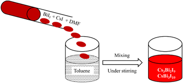 |
| | Fig. 1 Schematic representation of LARP process to synthesize Cs3Bi2I9/CsBi3I10 perovskite. | |
Device fabrication
Perovskite solar cells were fabricated on ITO-coated glass substrates with a sheet resistance of 15 Ω per square. The prepatterned ITO/glass substrates were cleaned using ultrasonication in acetone, and isopropanol each for 15 min. The wet-cleaned ITO/glass substrates were then dried using N2 stream and exposed to the UV ozone treatment for 15 min before the film deposition. A 30 nm thick NiOx HTL (hole transporting layer) was formed on the ITO surface by spin-coating at a rotation speed of 4000 rpm using NiOx precursor solution.19 The NiOx HTL was then annealed at 230 °C in air for 45 min. The NiOx-coated ITO/glass substrates were transferred into a nitrogen-purged glovebox, with oxygen and moisture levels below 0.1 ppm. The perovskite semiconductor films were formed by spin coating a precursor perovskite solution, dissolved in N,N-dimethylformamide at a concentration of 400 mg mL−1, on top of the NiOx layer at 4000 rpm for the 30 s. Then the spin-coated films were then annealed at 100 °C for 10 min. Then, PC61BM layer (20 mg mL−1 in chlorobenzene) was deposited by spin coating at 2000 rpm for the 30 s. Next, the bathocuproine (BCP) interlayer was deposited using 80 μL of solution (0.05 wt% in isopropanol) by spin coating at 4000 rpm. Subsequently, a 100 nm thick Ag top electrode was deposited using thermal evaporation, with a deposition rate of 0.2 Å s−1, in a vacuum chamber. The perovskite solar cells have an active area of 5.0 × 2.0 mm2.
Characterization and measurements
The crystal structures of Cs3Bi2I9 and CsBi3I10 were acquired by employing a Bruker D8 diffractometer using Cu Kα radiation (λ = 1.54 Å) at a scan rate of 0.02° min−1. The morphological studies were analyzed by JEOL 7401F scanning electron microscope. A Specord S 600 diode array UV-visible spectrometer was employed to record diffuse reflectance spectroscopy. The current density–voltage measurements of the perovskite devices were carried out using a 1 kW Oriel solar simulator with an AM 1.5G filter as the light source in conjunction with a Keithley 2400 source measurement unit. Solar measurements were carried out under 1000 W m−2 AM 1.5G illumination conditions. For accurate measurement, the light intensity was calibrated using a reference silicon solar cell (PV Measurements Inc.) certified by the National Renewable Energy Laboratory. Device fabrication and characterizations were performed in a glove box without any encapsulation. The photovoltaic parameters are derived from J–V plot, and FF was calculated using the following equation, FF = Jmpp × Vmpp/JSC × VOC. where, Jmpp and Vmpp and current density and voltage at maximum power point condition.
Results and discussions
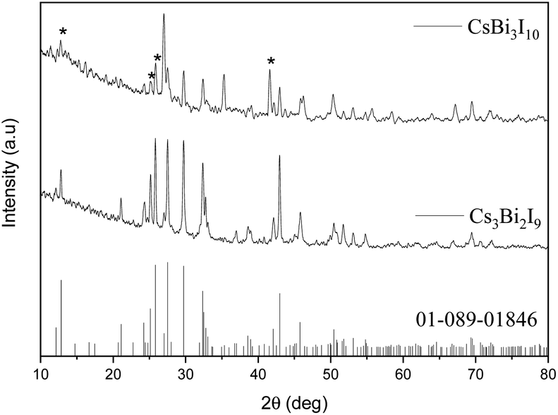
The XRD pattern of both Cs3Bi2I9 and CsBi3I10 are shown in Fig. 2. The formation of Cs3Bi2I9 has been compared with the available JCPDS card no. 01-089-1846, whereas the crystal system of the CsBi3I10 has been compared with the previously reported literature,15 since JCPDS card no. for reference pattern of CsBi3I10 is not available.
 |
| | Fig. 2 XRD pattern of Cs3Bi2I9/CsBi3I10 compared with the JCPDS card no. 01-089-1846 (* denote most significant peaks). | |
The XRD pattern of Cs3Bi2I9 shown in Fig. 3, reveals that the crystal structure belongs to a hexagonal geometry (space group P63/mmc) with the lattice constants of a = 8.40, b = 8.40, c = 21.24 Å (JCPDS card no. 01-089-1846) having two Bi3+ ions in the unit cell. The face sharing of two [BiI6]3− octahedra forms and [Bi2I9]3− bi-octahedra eventually ended with the 0-D crystal structure. The Cs+ ions fill the voids present in those bi-octahedra.16 The peaks observed at 12.8°, 21.1°, 24.3°, 25.1°, 25.8°, 27.5°, 29.7°, 32.3°, 36.9°, 38.5°, 42.1°, 42.9°, 45.8°, 50.4°, 51.7°, 53.0°, 54.8°, 69.4° are corresponding to the planes of (1 0 1), (1 1 0), (1 0 5), (0 0 6), (2 0 2), (2 0 3), (2 0 4), (2 0 5), (2 1 4), (2 0 7), (2 0 8), (2 2 0), (2 0 9), (2 2 6), (4 0 3), (4 0 4), (4 0 5), (3 3 4), respectively. The observed XRD pattern of the Cs3Bi2I9 well matches with the reference pattern (JCPDS card no. 01-089-1846), which confirms the formation of the same. The XRD pattern of CsBi3I10 reveals the most significant peaks (asterisk symbol shown in Fig. 2) at 12.8, 25.1, 25.8, 41.6 which correspond to the (0 0 3), (0 0 6), (1 1 5), (3 0 0) planes respectively. Further, many peaks corresponding to Cs3Bi2I9 have been found in the XRD pattern of CsBi3I10. It should be noted that the crystal structure of CsBi3I10 is comparable to the crystal structure of BiI3 and Cs3Bi2I9 which are stable secondary and ternary phases.17 In addition to this, the XRD pattern of CsBi3I10 deposited on the glass also confirms the presence of (0 0 3), (0 0 6), (1 1 5), (3 0 1) planes in the crystal lattice (Fig. S1†).
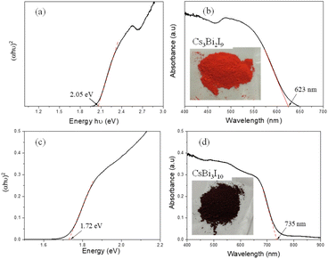 |
| | Fig. 3 (a, c) DRS and (b, d) absorption spectra of Cs3Bi2I9 and CsBi3I10 respectively, (inset photograph shows the respective perovskite samples). | |
The diffuse reflectance spectroscopy (DRS) of Cs3Bi2I9 shows (Fig. 3a) a bandgap of 2.05 eV which is in good agreement with the theoretically calculated bandgap value.18 The characteristic absorption peak at 488 nm has been observed in the UV-vis spectrum of Cs3Bi2I9 (Fig. 3b). The range of visible light absorption has been found to extend up to 623 nm. Compared to Cs3Bi2I9, the bandgap of CsBi3I10 has been reduced to 1.72 eV (shown in Fig. 3c), which causes extended light absorption. The absorption spectra of CsBi3I10 film recorded before (at room temperature) and after annealing (100 °C) are shown in Fig. S2a.† The dark colour of the CsBi3I10 layer can be visibly seen in the images shown in Fig. S2b and c (ESI†).
Morphological study
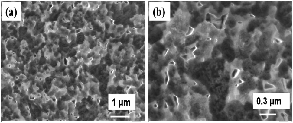
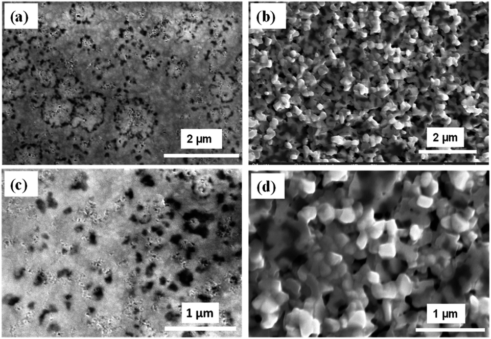
The FE-SEM images of Cs3Bi2I9 power with different magnifications are shown in Fig. 4a and b. The images show the morphology of the Cs3Bi2I9 appears to be hexagonal flakes-like shapes with low-dimension. The thickness of the flakes is found to be around 30 nm which is perpendicular to the surface. Further, the elemental presence of Cs, Bi, and I in Cs3Bi2I9 has been confirmed from the EDX image shown in Fig. S3.† The surface morphology of the CsBi3I10 films after annealing show the well-defined perovskite crystal with enhanced morphology (Fig. 5a–d). The EDX image of both Cs3Bi2I9 (powder) and CsBi3I10 perovskite film layer (after annealing at 100 °C) shown in Fig. S3† confirm the elemental presence of the components Cs, Bi, and I, respectively. The difference in the stoichiometry ratio (Fig. S3a†) might be due to the presence of secondary and ternary phase in the sample. The presence of indium and silicon (Fig. S3b†) element along with Cs, Bi, and I comes from the ITO/glass substrate (since EDX has been recorded for CsBi3I10 film coated on glass/ITO substrate after annealing 100 °C).
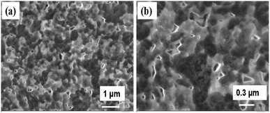 |
| | Fig. 4 (a and b) SEM images of Cs3Bi2I9. | |
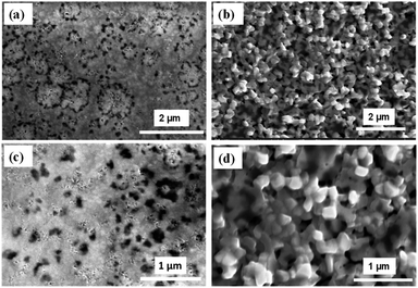 |
| | Fig. 5 (a, c) SEM images of CsBi3I10 film before annealing (b, d) after annealing. | |
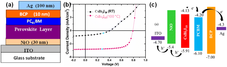
J–V characterization
The schematic representation of the device structure is shown in Fig. 6a. J–V measurements of the perovskite solar cell devices fabricated with Cs3Bi2I9, and CsBi3I10 (before and after annealing) have been depicted in Fig. 6b and the J–V parameters are shown in Table 1. The device structure adopted in this work is ITO/NiOx/perovskite layer/PC61BM/BCP/Ag. As shown in Fig. 6b, the device fabricated with Cs3Bi2I9 delivered a power conversion efficiency (PCE) of 0.7% with a FF of 47, VOC of 0.62 V, and JSC of 2.4 mA cm−2. The poor performance of the device might be due to the discrete nature of the [Bi2I9]3− bioctahedra as well as bulk recombination even though Cs3Bi2I9 has a long charge carrier lifetime.16 The device fabricated with CsBi3I10 before annealing delivered the PCE of 0.15% with FF of 34%, VOC of 0.40 V, and JSC of 1.1 mA cm−2. The poor performance of the device is due to the absence of perovskite structure formation. Finally, the device fabricated with annealed CsBi3I10 showed the best performance efficiency of 2.3% with improved FF of 69%, VOC of 0.79 V, and JSC of 4.2 mA cm−2. Upon annealing 100 °C, the CsBi3I10 film changes color from orange-red to blackish (Fig. S2–c†) with compact and large grain morphology. Compared to Cs3Bi2I9, the enhanced performance of CsBi3I10 perovskite-based device due to improved surface morphology, reduced interface energy barrier, and efficient interfacial charge extraction.16 In addition to this, the broader light absorption of CsBi3I10 compared to Cs3Bi2I9 which is evidenced by the UV-vis absorption spectra shown in Fig. 3d, enhances the generation of photocurrent of the CsBi3I10-based perovskite solar cell device. Furthermore, the usage of the BCP layer in the device architecture facilitates hole blocking with enhanced electron extraction at the cathode (PCBM/BCP/Ag) interface.12
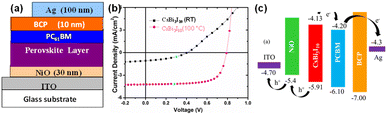 |
| | Fig. 6 (a) Schematic of perovskite solar cell (b) J–V measurements of perovskite devices fabricated with CsBi3I10 (before and after annealing) and (c) energy level diagram of device components of perovskite solar cell. | |
Table 1 Device characteristics of perovskite solar cells fabricated with Cs3Bi2I9 and CsBi3I10
| Perovskite layer |
JSC (mA cm−2) |
VOC (V) |
FF (%) |
PCE% |
| Cs3Bi2I9 (before annealing) |
2.2 |
0.60 |
45 |
0.60 |
| Cs3Bi2I9 (after annealing) |
2.4 |
0.62 |
47 |
0.70 |
| CsBi3I10 (before annealing) |
1.1 |
0.40 |
34 |
0.15 |
| CsBi3I10 (after annealing) |
4.2 |
0.79 |
69 |
2.30 |
Modifying the surface morphology and the film quality are most common way to improve the device performance.6 In this regard, researchers attempted to fabricate the CsBi3I10 film via spin coating and thermal annealing process to improve the surface morphology. In this work, the CsBi3I10 perovskite prepared from LARP assisted synthesis shows well-defined perovskite crystal with hexagonal flakes-like morphology which is desirable for the device performance. The results from this work reveal that LARP assisted synthesis can improve the film quality and morphology. Further, the utilization of hole extraction layer (NiOx nanoparticle) and hole blocking layer (BCP) facilitate the extraction of electron at the electrode interface12 which simultaneously enhances the overall performance of the device. The Cs3Bi2I9 and CsBi3I10 perovskite-based solar cell performances of the previously reported literature have been compared and shown in Table S1 (ESI†). It is evidenced that the CsBi3I10 perovskite synthesized via the LARP approach delivered the best overall performance along with improved FF among all the previous reports.
Conclusions
Herein, we demonstrated the LARP approach to the synthesis of highly efficient CsBi3I10 perovskite for solar cell application. The XRD pattern of CsBi3I10 showed the presence of secondary and ternary phases within it. The SEM images of CsBi3I10 showed improved morphology and crystallinity compared to Cs3Bi2I9. The device based on CsBi3I10 showed the best overall performance efficiency of 2.3%. The device fabricated with Cs3Bi2I9 showed a PCE of only 0.7%. The presence of excess BiI3 in the CsBi3I10 improved the performance efficiency by suppressing the intrinsic defects of the device. The higher absorption of CsBi3I10 in the extended UV-vis region compared to Cs3Bi2I9 helped to improve the JSC value of the device. Further, the device architecture ITO/NiOx/perovskite layer/PC61BM/BCP/Ag in which the BCP helps to block the unwanted hole leakage at the CsBi3I10/PCBM interface by improving the charge transport process in the device. This work paves the way to achieving high-performance CsBi3I10 perovskite solar cells.
Conflicts of interest
There are no conflicts to declare.
Acknowledgements
Author SV thanks the DST-WOS-A (SR/WOS-A/CS-78/2017). Author SA thanks the SPARC scheme (SPARC/2018-2019/P236/SL) for the financial assistance. JS and DJJ acknowledge the support of the Australian Government through the Australian Renewable Energy Agency (ARENA) and the Australian Centre for Advanced Photovoltaics (ACAP). The Australian Government does not accept responsibility for the views, information or advice expressed herein.
References
- J. Deng, L. Yang, X. Zhang, K. Wei, G. Du, G. Zhu and J. Zhang, J. Mater. Chem. A, 2022, 10(17), 9384–9392 RSC.
- J. Shamsi, A. S. Urban, M. Imran, L. De Trizio and L. Manna, Chem. Rev., 2019, 119(5), 3296–3348 CrossRef CAS PubMed.
- J. Kang, J. Liu, O. Allen, M. Al-Mamun, P. Liu, H. Yin, Y. Wang, S. Chen and H. Zhao, Energy Technol., 2022, 10(7), 2200318 CrossRef CAS.
- D. B. Khadka, Y. Shirai, M. Yanagida and K. Miyano, J. Mater. Chem. C, 2019, 7(27), 8335–8343 RSC.
- B. W. Park, B. Philippe, X. Zhang, H. Rensmo, G. Boschloo and E. M. Johansson, Adv. Mater., 2015, 27(43), 6806–6813 CrossRef CAS PubMed.
- J. Shin, M. Kim, S. Jung, C. S. Kim, J. Park, A. Song, K. B. Chung, S. H. Jin, J. H. Lee and M. Song, Nano Res., 2018, 11(12), 6283–6293 CrossRef CAS.
- B. B. Yu, M. Liao, J. Yang, W. Chen, Y. Zhu, X. Zhang, T. Duan, W. Yao, S. H. Wei and Z. He, J. Mater. Chem. A, 2019, 7(15), 8818–8825 RSC.
- M. B. Johansson, B. Philippe, A. Banerjee, D. Phuyal, S. Mukherjee, S. Chakraborty, M. Cameau, H. Zhu, R. Ahuja, G. Boschloo and H. Rensmo, Inorg. Chem., 2019, 58(18), 12040–12052 CrossRef CAS PubMed.
- M. B. Johansson, H. Zhu and E. M. Johansson, J. Phys. Chem. Lett., 2016, 7(17), 3467–3471 CrossRef CAS PubMed.
- X. Y. Chen, H. B. Lan, G. X. Liang and P. Fan, Photonics for Energy, Optica Publishing Group, 2018, p. PT4B-28 Search PubMed.
- M. Karim, K. Matsuishi, T. H. Chowdhury, W. I. Chowdhury, M. Abdel-shakour and A. Islam, J. Mater. Sci.: Mater. Electron., 2022, 33(10), 8114–8126 CrossRef CAS.
- P. Mariyappan, T. H. Chowdhury, S. Subashchandran, I. Bedja, H. M. Ghaithan and A. Islam, Sustainable Energy Fuels, 2020, 4(10), 5042–5049 RSC.
- R. F. Ali, I. Andreu and B. D. Gates, Nanoscale Adv., 2019, 1(11), 4442–4449 RSC.
- J. Shamsi, A. S. Urban, M. Imran, L. De Trizio and L. Manna, Chem. Rev., 2019, 119(5), 3296–3348 CrossRef CAS PubMed.
- P. Sebastia-Luna, M. C. Gélvez-Rueda, C. Dreessen, M. Sessolo, F. C. Grozema, F. Palazon and H. J. Bolink, J. Mater. Chem. A, 2020, 8(31), 15670–15674 RSC.
- B. Ghosh, B. Wu, H. K. Mulmudi, C. Guet, K. Weber, T. C. Sum, S. Mhaisalkar and N. Mathews, ACS Appl. Mater. Interfaces, 2018, 10(41), 35000–35007 CrossRef CAS PubMed.
- X. W. Tong, Z. X. Zhang, D. Wang, L. B. Luo, C. Xie and Y. C. Wu, J. Mater. Chem. C, 2019, 7(4), 863–870 RSC.
- K. M. McCall, C. C. Stoumpos, O. Y. Kontsevoi, G. C. Alexander, B. W. Wessels and M. G. Kanatzidis, Chem. Mater., 2019, 31(7), 2644–2650 CrossRef CAS.
- Z. Liu, J. Chang, Z. Lin, L. Zhou, Z. Yang, D. Chen, C. Zhang, S. Liu and Y. Hao, Adv. Energy Mater., 2018, 8(19), 1703432 CrossRef.
Footnotes |
| † Electronic supplementary information (ESI) available: XRD, absorption spectra, of CsBi3I10 film. EDX of Cs3Bi2I9. Comparison table. See DOI: https://doi.org/10.1039/d3ra00365e |
| ‡ Equally contribute. |
|
| This journal is © The Royal Society of Chemistry 2023 |
Click here to see how this site uses Cookies. View our privacy policy here. 
 Open Access Article
 This Open Access Article is licensed under a Creative Commons Attribution-Non Commercial 3.0 Unported Licence
 ab,
Jegadesan Subbiah*c,
David J. Jones
ab,
Jegadesan Subbiah*c,
David J. Jones