
 Open Access Article
 This Open Access Article is licensed under a Creative Commons Attribution-Non Commercial 3.0 Unported Licence
Characterization and study of high conductivity antimony-doped tin oxide thin films grown by mist chemical vapor deposition
Li Liu *a,
Mariko Uedab and
Toshiyuki Kawaharamuraabc
*a,
Mariko Uedab and
Toshiyuki Kawaharamuraabc
aSchool of System Engineering, Kochi University of Technology, 185 Miyanokuchi, Tosayamada, Kami, Kochi 782-8502, Japan. E-mail: liu.li@kochi-tech.ac.jp; kawaharamura.toshiyuki@kochi-tech.ac.jp
bIntelligent Mechr. Sys. Eng. Course, Kochi University of Technology, 185 Miyanokuchi, Tosayamada, Kami, Kochi 782-8502, Japan
cResearch Institute, Kochi University of Technology, 185 Miyanokuchi, Tosayamada, Kami, Kochi 782-8502, Japan
First published on 2nd May 2023
Abstract
Antimony doped tin oxide thin films are grown at atmospheric pressure using a home-built mist chemical vapor deposition system, which is an environmental-friendly technique with low energy consumption. For obtaining high quality Sb:SnOx films, different solutions are used to support the film fabrication process. The role of each component in supporting solution is also preliminarily analyzed and studied. In this work, the growth rate, density, transmittance, hall effect, conductivity, surface morphology, crystallinity, component and chemical states of Sb:SnOx films are investigated. Sb:SnOx films prepared at 400 °C using a mixing solution of H2O, HNO3 and HCl show a low electrical resistivity of 6.58 × 10⁻⁴ Ω cm, high carrier concentration of 3.26 × 1021 cm−3, high transmittance of 90%, and wide optical band gas of 4.22 eV. X-ray photoelectron spectroscopy analyses disclose that the samples with good properties have high [Sn4+]/[Sn2+] and [O–Sn4+]/[O–Sn2+] ratios. Moreover, it is discovered that supporting solutions also affect the CBM–VBM level and Fermi level in the band diagram of thin films. These experimental results confirm that Sb:SnOx films grown using mist CVD are a mixture of SnO2 and SnO. The sufficient supply of oxygen from supporting solutions leads to the stronger combination of cations and oxygen, and the combination of cations and impurities disappear, which is one of the reasons for obtaining high conductivity Sb:SnOx films.
Introduction
Tin oxide (SnO2) thin film is known as a promising material for transparent conducting oxide films (TCOs) because of its outstanding photoelectric properties, high chemical stability and good heat resistance.1,2 Especially the tin related oxide thin films, such as indium tin oxide (In2O3![[thin space (1/6-em)]](https://www.rsc.org/images/entities/char_2009.gif) :SnO2 = 9:1); ITO, fluorine doped tin oxide (SnO2:F); FTO, and antimony doped tin oxide (SnO2:Sb); ATO, exhibit lower resistivity (10−3 to 10−4 Ω cm) and higher transmittance (>80%) in the visible region (390–780 nm).3–5 Among these tin related oxide films, ATO is a candidate doping material with the potential to be studied because the Sb precursor is usually chemically-stable, earth-abundant and non-toxic.6,7
:SnO2 = 9:1); ITO, fluorine doped tin oxide (SnO2:F); FTO, and antimony doped tin oxide (SnO2:Sb); ATO, exhibit lower resistivity (10−3 to 10−4 Ω cm) and higher transmittance (>80%) in the visible region (390–780 nm).3–5 Among these tin related oxide films, ATO is a candidate doping material with the potential to be studied because the Sb precursor is usually chemically-stable, earth-abundant and non-toxic.6,7
However, compared with ITO and FTO films, which have been obtained easily with low resistivity of ∼10−4 Ω cm, the higher resistivity limits the wide application of ATO films in many fields. According to previous studies, ATO thin films have been prepared using various techniques, such as sputtering,8 pulsed-laser deposition,9 metal–organic chemical vapor deposition,10 aerosol assisted chemical vapor deposition,11 and spray pyrolysis.12 With the continuous improvement of fabrication techniques, the ATO films with resistivity in the order of ∼10−4 Ω cm can be obtained using high growth temperature, highly active precursors, or the subsequent annealing treatment.10,13
In this work, ATO thin films were prepared using the 3rd generation mist CVD system, which has a special supply unit including two or more solution chambers and one mixing chamber, and a special reactor with the fine channel (FC) structure. This fine channel type reactor has excellent control over the mist flow for fabricating uniform and high-quality thin films on a large-area substrate under atmospheric pressure. This precious control of mist flow, which makes mist CVD different from spray and AACVD techniques, is achieved by the following physics: the existence of Leidenfrost state droplets (ELSD) and the low probability of collisions between mist droplets (LPCD).14–18 As reported in some of the literature, the 2nd and 3rd generation mist CVD has been used to fabricate several metal oxide films.19–23
Moreover, in contrast to previous research, which improved the film conductivity by optimizing doping ratio and/or increasing growth temperature, we used several liquid materials to support the fabrication process. These liquid materials are called “supporting solution”, as they are different from the catalysts and react with the precursors in the reactor. In the experiment, ATO thin films were prepared using different supporting solutions. By summarizing and analyzing the experimental results, it was found that the ATO films were mixture of SnO and SnO2, and the combination of H2O, HNO3 and HCl promoted the formation of SnO2 by increasing the [Sn4+]/[Sn2+] ratio and [O–Sn4+]/[O–Sn2+] ratio, and affected the conductivity, which has never previously been reported.
Experiments
ATO thin films were deposited on quartz under atmospheric pressure by the 3rd generation mist CVD with two solution chambers at 400 °C. Tin(II) chloride dihydrate (SnCl2·2H2O) and antimony(III) chloride (SbCl3) were dissolved in methanol simultaneously (Sb doping ratio was 1.6%) and added to one solution chamber of mist CVD system, while supporting solutions were made with different combinations of H2O, HNO3 (69%) and HCl (35.0–37.0%), and were added to the other solution chamber. The detailed growth conditions were shown in Table 1. Quartz substrates were cleaned by sequential sonication in the acetone, isopropanol, and deionized water for 2 min each to remove the surface contamination, and O3 gas (5000 ppm of O3 in 1.5 L per min O2) was used to remove the hydrogen and carbon residues on quartz surface for 2 min at growth temperature. N2 was chosen as the carrier gas and dilution gas to transport the mist from solution chambers to reactor.| A | B | C | D | ||
|---|---|---|---|---|---|
| a Precursor solution chamber.b Supporting solution chamber.c Carrier gas/dilution gas. | |||||
| Ch. 1a | Solute concentration | SnCl2·2H2O, SbCl3 50 mM, 0.8 mM | |||
| Solvent | MeOH | ||||
| Ch. 2b | Supporting solution (composition ratio) | × | H2O only | H2O, HNO3 (99.2:0.8) |
H2O, HNO3, HCl (98.7:0.8:0.5) |
| Substrate | 30.0 × 30.0 × 0.5 mm3 Quartz | ||||
| c.g/d.gc of sol. Ch. 1, L min−1 | 5.0/0.0 | ||||
| c.g/d.g of sol. Ch. 2, L min−1 | 2.0/3.0 | ||||
| Growth temperature, °C | 400 | ||||
| Growth system | Fine-channel & three-sol.-ch. type mist CVD system | ||||
| Ultrasonic transducer | 2.4 MHz, 24 V × 0.6 A, 3 | ||||
A spectroscopic ellipsometer (J. A. Woollam, W-VASE) was employed to estimate the film thickness (t) and refractive index (n) using the Cauchy model in the transparent region. Sheet resistance (Rs) was studied by a Hall effect setup in the Van der Pauw configuration, the electrical resistivity (R) and conductivity (σ) were determined by the relations: R = Rs × t and σ = 1/R. Optical transmittance of sample was measured in the range of 176–2500 nm using UV-Visible spectrometer (Hitachi UV-Vis U-4100). Surface morphology of thin film was measured by Atomic Force Microscope (AFM, Pacific technology Nano-RJ). The crystal structure was analyzed by the X-ray diffraction (XRD) and grazing incident X-ray diffraction (GIXD) using the CuKα radiation (X-ray wavelength λ = 1.5418 Å, incident angle 0.35°, Rigaku SmartLab). X-ray reflectivity (XRR) was carried out to evaluate the density of thin films. X-ray photoelectron spectroscopy (XPS, AXIS Ultra DLD) was used to investigate the valence states of Sn, the monochromatic Al-Kα (hν = 1486.7 eV) X-ray source was operated at 40 W and 8 kV at room temperature, and the operating pressure was <3.0 × 10⁻⁸ Pa. The binding energies in XPS spectra were calibrated in terms of the peak position of C 1s spectra appearing at 284.8 eV for adventitious carbon surface contamination.24,25 Ionization energy was measured by photoelectron yield spectroscopy (PYS) (BIP-KV202GD/UVT, Bunkoukeiki Co., Ltd), in which a D2 lamp and photo multiplier were used as a light source and detector, respectively.
Results
In order to precisely study the effects of different supporting solutions on the ATO films, the thicknesses of samples were maintained at approximately 190 nm. However, the differences in film thickness still caused differences in colors. In addition, the different optical properties were also one of the reasons for the difference in film color. Although these four samples showed different colors, they had uniform surfaces without cracks over the whole region area of 30 × 30 mm2, as shown in Fig. 1.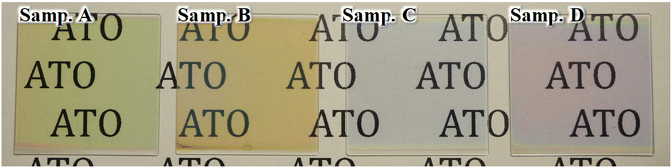 | ||
| Fig. 1 Photos of ATO films prepared using different supporting solutions. | ||
Table 2 and Fig. 2 summarized the effects of different supporting solutions on the film deposition rate, refractive index, density and electrical properties. In Fig. 2(a), ATO films prepared with H2O (sample B) has lower growth rate than the film prepared without supporting. Moreover, sample C and D show lower deposition rates compared to sample B. The film density obtained by XRR measurement is shown in Fig. 2(b). It can be seen that the film density increased from 5.1 g m−3 (sample A) to 6.3 g m−3 (sample B) by using H2O support. For sample C and D, HNO3 and HCl further increased the density to nearly 7.0 g m−3. The decrease in deposition rate and increase in film density are likely due to the use of H2O as an oxygen source, which reduces the impurities during film formation. Considering that HNO3 and HCl were used in the preparation of sample C and D, it was deduced that slight acid corrosion from HNO3 and HCl in supporting solutions affected the deposition rate of films. Fig. 2(c) shows the refractive index of four samples. Typically, the refractive index of pure SnO2 is 1.90–2.10.26–28 In this study, the refractive index value (in 550 nm) of sample prepared without support was 2.078, which was larger than that of sample B (n = 2.002), C (n = 1.993) and D (n = 1.984). These results clearly show that the film properties are improved by the supporting solutions.
| A | B | C | D | |
|---|---|---|---|---|
| Deposition rate (nm min−1) | 50.9 | 32.8 | 19.9 | 22.7 |
| Density (g cm−3) | 5.1 | 6.3 | 6.7 | 6.9 |
| Refractive index | 2.078 | 2.002 | 1.993 | 1.984 |
| Resistivity (Ω cm) | 9.50 × 10⁻¹ | 4.85 × 10⁻³ | 6.86 × 10⁻⁴ | 6.58 × 10⁻⁴ |
| Carrier concentration (cm3) | 3.19 × 10¹⁹ | 1.79 × 10²¹ | 2.85 × 10²¹ | 3.26 × 10²¹ |
| Hall mobility (cm2 V−1 s−1) | 0.20 | 0.72 | 3.20 | 2.92 |
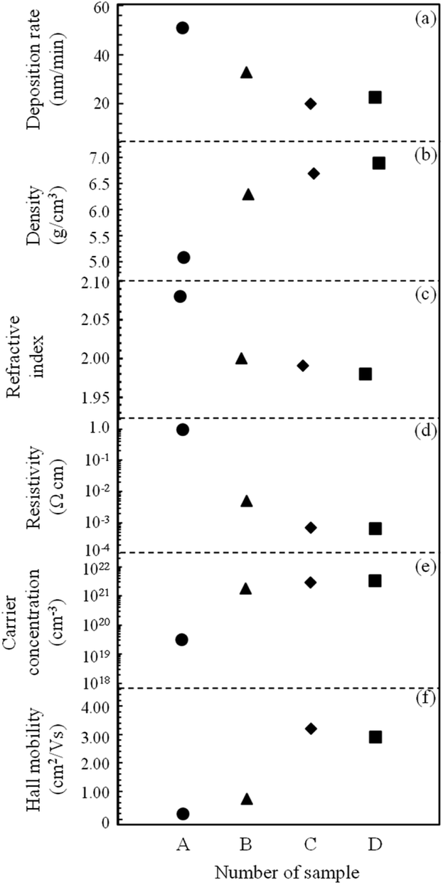 | ||
| Fig. 2 Summary of (a) deposition rate, (b) density, (c) refractive index and (d), (e), (f) electrical properties of ATO films prepared with different supporting solutions. | ||
Fig. 2(d)–(f) summarize the electrical properties of SnOx:Sb thin films growth using different supporting conditions. In Fig. 2(d), it can be seen that the resistivity significantly decreased from 9.50 × 10⁻¹ Ω cm (sample A) to 4.85 × 10⁻³ Ω cm (sample B) while using H2O to support the fabrication. When H2O + HNO3 (sample C) and H2O + HNO3 + HCl (sample D) were used, the resistivity decreased to 6.84 × 10⁻⁴ Ω cm and 6.58× 10⁻⁴ Ω cm respectively, that was dramatically lower than that of sample B. The decrease in resistivity was always accompanied by increasing carrier concentration (n) and Hall mobility (μ), a result consistent with ref. 10, in which it was reported that the film resistivity was associated with the carrier density and Hall mobility. According to previous research, it can be known that Sb may exist in two distinct oxidation states of Sb3+ and Sb5+ in Sb-doped SnO2 films.29–31 When the films prepared without supporting solution, Sb mainly existed in Sb3+. With the use of supporting solutions, Sb3+ were oxidized to Sb5+, and the Sb5+ replaced on Sn4+ sites operated as donor and contributed additional free electrons.32,33 This substitution phenomenon caused the decrease in film resistivity for sample B–D. Obviously, as one kind of oxygen source, H2O played an important role in reducing the resistivity. HNO3 and HCl were absolutely necessary for further reducing the resistivity of ATO films by acting as oxidants in the conversion Sb3+ state to Sb5+ state. R. L. Rich also concluded that the Sb3+ compounds can be oxidized to Sb5+ by HNO3 in previous research.34
In addition to the electrical properties, optical characteristics are also important for high-quality ATO thin films. Fig. 3 shows the optical transmittance spectra of sample A–D prepared on transparent quartz substrates, these spectra in Fig. 3 have deducted that of quartz substrate. The thin films fabricated without supporting solution (sample A) had the lowest average transmittance of ∼82% in the visible region (390–780 nm). For samples B, C and D, which were prepared using different supporting conditions, the average transmittances were near 90%. This result illustrates that the supporting solutions are propitious to obtaining the high transparent ATO thin films, while the similar average transmittance of sample B, C and D proves that the effect of H2O on the transparent is bigger than that of HNO3 and HCl. In the infrared region (wavelength is greater than 780 nm), the transmittances of sample B, C and D showed a common tendency in that the transmittance decreased with an increase in the wavelength. Considering that the carrier density of sample B, C and D were larger than that of sample A (in Fig. 2(e)), it was determined that the degradation of transmittance in the infrared region was caused by the free-carrier electro-reflection, which also was found in ref. 35. Moreover, the optical band gaps (Eg) of sample A (Eg = 3.52 eV), B (Eg = 4.08 eV), C (Eg = 4.20 eV) and D (Eg = 4.22 eV) were also calculated using the relationship (αhν)2 ∝ (hν − Eg).36,37 According to previous research, the large Eg values of sample B, C and D were usually caused by the Burstein–Moss effect, which is an apparent effect of the band gap extend caused by the high carrier concentration filling in the orbit.38,39 In short, the differences in optical band gaps come from the following relationship: Eg = Eg0 + ΔEMB, where Eg0 is the intrinsic band gap and ΔEMB is the Burstein–Moss effect.
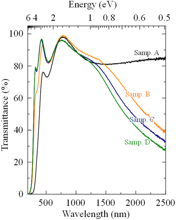 | ||
| Fig. 3 Optical transmittance spectra of ATO thin films fabricated with different supporting solutions. | ||
The surface morphology and crystal structure of samples were confirmed by atomic force microscope and X-ray diffractometer, shown in Fig. 4(a) and (b). In Fig. 4(a), it can be seen that all the ATO films were uniform and without cracks. The sample A, prepared without supporting solution, showed a smooth surface with the root mean square (RMS) roughness of 1.76 nm, which was smaller than that of sample B, C and D. In the images of sample B, C and D, the distribution of obvious grains was continuous and regular on the surface, which reduced the scattering effect, and increased in the transmittance of thin films.
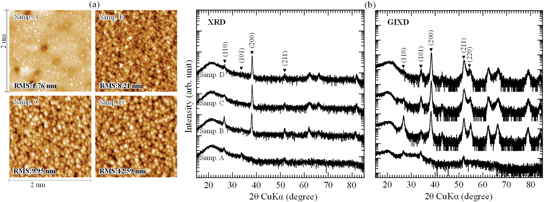 | ||
| Fig. 4 (a) AFM images and (b) XRD, GIXD spectra of ATO films fabricated with different supporting solutions. | ||
Fig. 4(b) depicts the XRD and GIXD patterns of ATO films. There were small diffraction peaks (110), (101) and (211) appeared in the XRD and GIXD spectra of sample A, indicating that the ATO films prepared by 3rd G mist CVD system had polycrystalline structure. When H2O was used to support the fabrication process (sample B), the crystallinity was changed. The intensity of peak (110) increased. New preferred peak (200) appeared in the XRD and GIXD spectra, a peak that was also reported in ref. 1, 9, 12 and 40. For sample C and D, the intensity of preferred peak (200) increased and that of peak (110) reduced. Moreover, a slight right shift of peak (200) also appeared in sample C and D. This shift may be caused by the increasing atomic ratio of Sb in the films, which was deduced to be promoted by the HNO3 in supporting solution.
Components and chemical states of ATO films were confirmed by the Sn 3d5/2, O 1s and VB edge XPS spectra with Gaussian deconvoluted curves, and shown in Fig. 5(a)–(c). According to the XPS-peak-differentiation-imitating analysis of corresponding Sn 3d5/2 and O 1s peaks, the atoms of Sn exist at three components corresponding to the Sn4+ (BE = 486.8 eV), Sn2+ (BE = 486.2 eV) and Sn0 (BE = 484.8 eV), the O atoms also exist at three components of the O–Sn4+ at 530.4 eV, and O–Sn2+ at 529.8 eV, OChem at 531.8 eV, respectively.41 The existence of different valence states of Sn atoms indicated that the ATO thin films obtained by mist CVD were built-up essentially as a mixture of SnO and SnO2. In Fig. 5(a) it is clear that the supporting solution increased the [Sn4+]/[Sn2+] ratio. Compared with that of sample B and C, the [Sn4+]/[Sn2+] ratio of sample D which prepared by supporting solution including H2O, HNO3 and HCl increased slightly. In Fig. 5(b), H2O obviously increased the intensity of O–Sn4+ component and decreased the intensity of O–Sn2+ and OChem components, proving that H2O was a strong oxygen source in the fabrication of ATO films. When a mixture of H2O and HNO3 was used as supporting solution (sample C), the intensity of O–Sn2+ component was further decreased. For sample D, the existence of HCl further reduced the amount of OChem component. XPS results show that the combination of Sn4+ and O was improved by the support of H2O, HNO3, and HCl + HNO3, and the improvement tendency may be clarified by the strength of oxidation.
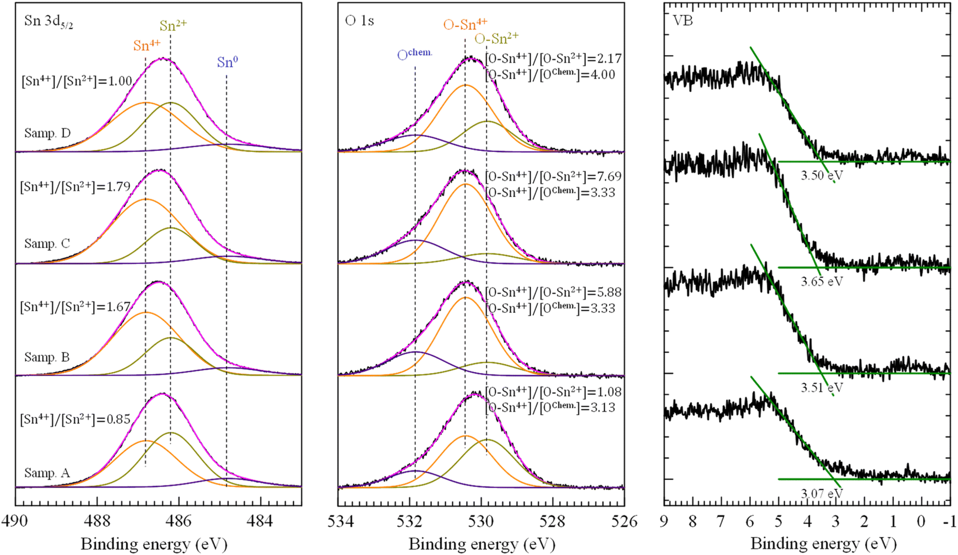 | ||
| Fig. 5 XPS spectra of Sn 3d5/2, O 1s and VB obtained from ATO thin films fabricated with different supporting solutions. | ||
In Fig. 5(c), the values of valence band maximum (VBM) were quantified by extrapolating the leading edge of valence band (VB) spectra to intersect with the background base line. It can be clearly seen that sample B, C, and D show high VBM value, which was attributed to Burstein-Moss effect caused by the large carrier density.42,43
Fig. 6(a) shown the PYS results of ATO films obtained using different supporting solutions. The measured ionization energy (IE) of sample A is 7.97 eV, while for sample B, C, and D, that value is 8.10 eV. By summarizing and analyzing the optical band gap, VBM, and PYS results, the band diagram of samples is obtained, as shown in Fig. 6(b). ECBM is the bottom of conduction band, EVBM is the top of valence band. The supporting materials obviously affected the CBM–VBM level and the Fermi level (EF). The influence of H2O on the band diagram is stronger than that of HNO3 or HCl + HNO3, proving that the H2O works as an oxygen source, which is important in the fabrication of high quality ATO films. Moreover, similarly to the H2O, HNO3 also changes the valence state of Sn, which can be seen from the change of Fermi level of sample C. For HCl, it is more likely to remove the impurities on the sample surface. In the near future, more experiments and studies are necessary to confirm the roles of HCl and HNO3 in the change of band diagram.
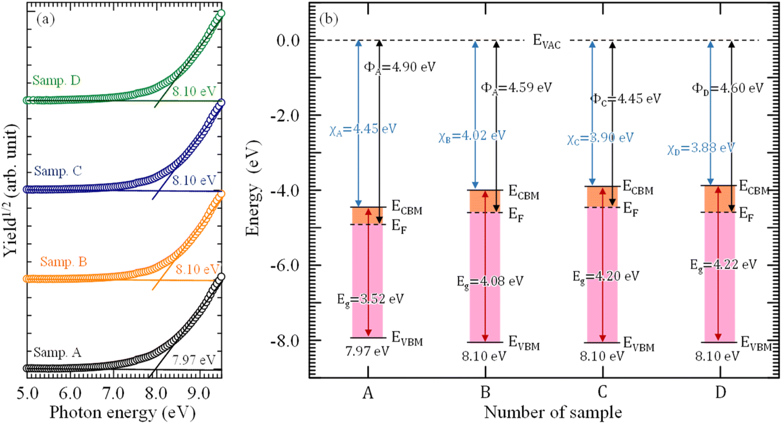 | ||
| Fig. 6 (a) PYS spectra and (b) energy band diagram of ATO films fabricated with different supporting solutions. Φ is work function, χ is electron affinity, Eg is optical band gap. | ||
Conclusions
In summary, fabrication of highly conductive thin films with good performances was achieved by 3rd G mist CVD system using different supporting solutions. To study the effects of different supporting materials on the properties of high quality ATO films, the electrical property, optical property, surface morphology, crystal structure, element chemical state in films and band diagram of samples prepared using different supporting solutions were investigated. Experimentally, the following results are obtained:1. H2O was an oxygen source, playing an important role in reducing the resistivity; HNO3 and HCl further reduced the film resistivity, and when mixture solution of H2O, HNO3 and HCl were used as supporting solution, the film with low resistivity of 6.58 × 10⁻⁴ Ω cm was obtained.
2. The obtained ATO thin films have polycrystalline structure, H2O promoted the crystallinity of samples and HNO3 reduced the intensity of peak (110) clearly.
3. These ATO films fabricated by mist CVD system were a mixture of SnO and SnO2, for the samples prepared without supporting solution, the lack of oxygen source may cause the combination of cations and impurities; when H2O was used as supporting solution, the sufficient supply of oxygen source lead to the stronger combination of cations and oxygen, and the combination of cations and impurities disappeared.
4. The combination effects of H2O, HNO3 and HCl promoted the formation of SnO2 by increasing the [Sn4+]/[Sn2+] ratio and [O–Sn4+]/[O–Sn2+] ratio, decreasing the content of OChem components in thin films.
5. The analysis of band diagram illustrates that H2O can affect the CBM–VBM level and Fermi level; furthermore, HNO3 works as a strong oxidation and HCl may play a role in cleaning the impurities.
In future experiments, the roles of HCl in fabrication of high quality ATO films will be investigated, and the mechanism by which H2O, HNO3 and HCl support the formation of ATO film will also be analyzed and studied.
Conflicts of interest
There are no conflicts to declare.References
- T. M. Hammad and N. K. Hejazy, Int. Nano Lett., 2012, 2, 7–11 CrossRef.
- T. Minami, S. Takata, H. Sato and H. Sonohara, J. Vac. Sci. Technol., A, 1995, 13, 1095–1099 CrossRef CAS.
- Y. Ren, Q. H. Wang, X. G. Zhou, Y. Gao and G. Y. Zhao, J. Electron. Mater., 2017, 46, 6864–6869 CrossRef CAS.
- Y. Akita, Y. Miyake, H. Nakai, H. Oi, M. Mita, S. Kaneko, M. Mitsuhashi and M. Yoshimoto, Appl. Phys. Express, 2011, 4, 035201 CrossRef.
- S. H. Yu, L. H. Ding, C. Xue, L. Chen and W. F. Zhang, J. Non-Cryst. Solids, 2012, 358, 3137–3140 CrossRef CAS.
- F. Chen, J. Y. Wu, Q. Shen, J. M. Schoenung and L. M. Zhang, Mater. Sci. Forum, 2014, 783–786, 1973–1978 CAS.
- J. Montero, J. Herrero and C. Guillén, Sol. Energy Mater. Sol. Cells, 2010, 94, 612–616 CrossRef CAS.
- H. P. Dang, Q. H. Luc, T. Le and V. H. Le, J. Nanomater., 2016, 2016, 7825456 Search PubMed.
- S. H. Yu, W. F. Zhang, L. Li, D. Xu, H. L. Dong and Y. X. Jin, Appl. Surf. Sci., 2013, 286, 417–420 CrossRef CAS.
- X. J. Feng, J. Ma, F. Yang, F. Ji, F. J. Zong, C. N. Luan and H. L. Ma, Appl. Surf. Sci., 2008, 254, 6601–6604 CrossRef CAS.
- S. D. Ponja, B. A. D. Williamson, S. Sathasivam, D. O. Scanlon, I. P. Parkin and C. J. Carmalt, J. Mater. Chem. C, 2018, 6, 7257–7266 RSC.
- A. A. Yadav, Thin Solid Films, 2015, 591, 18–24 CrossRef CAS.
- M. N. Yusnidar, V. Fauzia, D. Handoko and L. Hanum, J. Phys.: Conf. Ser., 2017, 817, 012031 CrossRef.
- T. Kawaharamura, Jpn. J. Appl. Phys., 2014, 53, 05FF08 CrossRef.
- P. Rutthongjan, L. Liu, M. Nishi, M. Sakamoto, S. Sato, E. K. C. Pradeep, G. T. Dang and T. Kawaharamura, Jpn. J. Appl. Phys., 2019, 58, 035503 CrossRef CAS.
- T. Kawaharamura, G. T. Dang, L. Liu, E. K. C. Pradeep, M. Tatsuta, M. Furuta, Y. Suwa, S. Sato, Y. Nakasone, S. Yamaoki, M. Nishi, Y. Kobayashi, M. Sakamoto, and P. Rutthongjan, 64th JSAP Spring Meeting, 2017, p. 17a-502-10 Search PubMed.
- T. Kawaharamura, P. Rutthongjan, L. Liu, M. Nishi, M. Sakamoto, Y. Kobayashi, E. K. C. Pradeep, G. T. Dang, S. Sato, S. Yamaoki, Y. Nakasone, and M. Ueda, 78th JSAP Autumn Meeting, 2017, p. 7a-C17-2 Search PubMed.
- L. Liu, T. Kawaharamura, G. T. Dang, E. K. C. Pradeep, S. Sato, T. Uchida, S. Fujita, T. Hiramatsu, H. Kobayashi and H. Orita, Jpn. J. Appl. Phys., 2019, 58, 025502 CrossRef CAS.
- L. Liu, Y. Suwa, S. Sato, Y. Nakasone, M. Nishi, G. T. Dang, E. K. C. Pradeep and T. Kawaharamura, Jpn. J. Appl. Phys., 2017, 56, 04CJ02 CrossRef.
- T. Kawaharamura, H. Nishinaka, K. Kametani, Y. Masuda, M. Tanigaki and S. Fujita, J. Soc. Mater. Sci., 2006, 55, 153–158 CrossRef CAS.
- T. Igawa, K. Kaneko and S. Fujita, J. Soc. Mater. Sci., 2011, 60, 994–997 CrossRef CAS.
- H. J. Jeon, S. G. Lee, H. Kim and J. S. Park, Appl. Surf. Sci., 2014, 301, 358–362 CrossRef CAS.
- G. T. Dang, Y. Suwa, M. Sakamoto, L. Liu, P. Rutthongjan, S. Sato, T. Yasuoka, R. Hasegawa and T. Kawaharamura, Appl. Phys. Express, 2018, 11, 111101 CrossRef.
- T. Uchida, R. Jinno, S. Takemoto, K. Kaneko and S. Fujita, Jpn. J. Appl. Phys., 2018, 57, 040314 CrossRef.
- T. Kamimura, K. Sasaki, M. H. Wong, D. Krishnamurth, A. Kuramata, T. Masui, S. Yamakoshi and M. Higashiwaki, Appl. Phys. Lett., 2014, 104, 192104 CrossRef.
- D.-w. Choi and J.-S. Park, Surf. Coat. Technol., 2014, 259, 238–243 CrossRef CAS.
- J. Heo, S. B. Kim and R. G. Gordon, Chem. Mater., 2012, 22, 4599–4602 RSC.
- J. W. Elam, D. A. Baker, A. J. Hryn, A. B. F. Martinson, M. J. Pellin and J. T. Hupp, J. Vac. Sci. Technol. A, 2008, 26, 244–252 CrossRef CAS.
- C. A. Vincent, J. Electrochem. Soc., 1972, 119, 515–518 CrossRef CAS.
- E. Elangovan and K. Ramamurthl, Cryst. Res. Technol., 2003, 38, 779–784 CrossRef CAS.
- S. Gupta, B. C. Yadav, P. K. Dwivedi and B. Das, Mater. Res. Bull., 2013, 48, 3315–3322 CrossRef CAS.
- K. Derrar, M. Zaabat, N. Rouabah, R. Nazir, F. Hanini, A. Hafdallah, S. A. Khan, N. S. Alsaiari, K. Mohammedsaleh Katubi and K. M. Abualnaja, J. Mater. Sci.: Mater. Electron., 2022, 33, 10142–10153 CrossRef CAS.
- R. Ramarajan, M. Kovendhan, K. Thangaraju, D. P. Joseph and R. R. Babu, Appl. Surf. Sci., 2019, 487, 1385–1393 CrossRef CAS.
- R. L. Rich, Inorganic Reactions in water, Springer, Germany, 1st edn, 2008, p. 349 Search PubMed.
- S. Y. Lee and B. O. Park, Thin Solid Films, 2006, 510, 154–158 CrossRef CAS.
- V. Fauzia, M. N. Yusnidar, L. H. Lalasari, A. Subhan and A. A. Umar, J. Alloys Compd., 2017, 720, 79–85 CrossRef CAS.
- B. Stjerna, E. Olsson and C. G. Granqvist, J. Appl. Phys., 1994, 76, 3797–3817 CrossRef CAS.
- K. G. Saw, N. M. Aznan, F. K. Yam, S. S. Ng and S. Y. Pung, PLoS One, 2015, 10, e0141180 CrossRef CAS PubMed.
- S. C. Dixon, D. O. Scanlon, C. J. Carmalt and I. P. Parkin, J. Mater. Chem. C, 2016, 4, 6946–6961 RSC.
- M. N. Yusnidar, V. Fauzia, D. Handoko and L. Hanum, J. Phys.: Conf. Ser., 2017, 817, 012031 CrossRef.
- J. Szuber, G. Czempik, R. Larciprete, D. Koziej and B. Adamowicz, Thin Solid Films, 2001, 391, 198–203 CrossRef CAS.
- C. Ke, W. G. Zhu, Z. Zhang, E. S. Tok, B. Ling and J. S. Pan, Sci. Rep., 2015, 5, 17424 CrossRef CAS PubMed.
- Y. Dou, T. Fishlock, R. G. Egdell, D. S. L. Law and G. Beamson, Phys. Rev. B, 1997, 55, R13381 CrossRef CAS.
| This journal is © The Royal Society of Chemistry 2023 |