DOI:
10.1039/D2RA07981J
(Paper)
RSC Adv., 2023,
13, 4236-4248
Influence of time dependent laser-irradiation for tuning the linear–nonlinear optical response of quaternary Ag10In15S15Se60 films for optoelectronic applications
Received
14th December 2022
, Accepted 25th January 2023
First published on 1st February 2023
Abstract
The impact of laser irradiation on thin films results in multiple beneficial modifications of their structural, morphological, nonlinear–linear properties for optoelectronics applications. This work deals with the thermally evaporated Ag10In15S15Se60 films and post-laser irradiation to study the variations in structural and optical properties. The current investigation was carried out for different laser irradiation time durations such as 0, 10, 20, 30, and 60 minutes by 532 nm laser (2.34 eV). According to the X-ray diffraction analysis, all thin films have polycrystalline character. The change in the surface morphology after being exposed to the laser has been checked by FESEM, whereas the presence of constitutional elements has been verified by the EDX study. The related changes with laser irradiation in the optical properties, including both linear and nonlinear, were studied using UV-Vis spectroscopy data. The irradiation caused an enhancement in the transmission, and the absorption edge moved towards a lower wavelength, increasing the bandgap energy from 1.71 eV to 1.88 eV. The refractive index reduced as a result of the film's altered structure. The behaviour of the refractive index satisfies Moss's rule (Egn4 = const). The nonlinear refractive index, first-order and 3rd order nonlinear susceptibility, is found to be decreased with laser irradiation. The dielectric parameters are also observed to be decreased with irradiation. Considering all the alterations in its properties caused by irradiation, the Ag10In15S15Se60 sample could be a favourable material for various photonic devices.
1. Introduction
Nowadays, chalcogenides have huge attention among scientists because of their electrical and optical characteristics.1,2 For a variety of solid-state devices, the carrier production and recombination processes in chalcogenides are vitally influenced by the intrinsic defect states and lack of long-range order.3,4 The measurement of photoelectrochemical characteristics can give a detailed view of the defect states inside the bandgap as well as the higher photosensitivity of the materials.5,6 The selenium-based chalcogenide alloys are particularly beneficial due to their large crystallization temperature, higher hardness, better photosensitivity, and less aging influence. Se-based chalcogenide materials have recently been shown to possess electrical and photoelectrical characteristics.7–9 Despite the fact that selenium has drawbacks, such as a short life and limited sensitivity in its natural state, it has various commercial applications. Scientists have combined other elements like Ge, Ag, In, Sb, Bi, etc., with Se to solve these issues.10,11 Indium chalcogenide thin films (In–Te–Se), which could be used to switch volatile PCM devices, have been reported by Pandian et al.12 Furthermore, the chalcogenide materials having Ag are currently used in many applications like phase change memory and optoelectronic devices because of their fast crystallization and better thermal stability.13 Similarly, AgInS2, a ternary compound, demonstrates notable third-order nonlinear optical characteristics. The material also can be used for solar cell technology due to its higher absorption coefficient and bandgap value.14 Considering the wide applications in the mentioned materials, it is worth investigating the quaternary In15Ag10S15Se60 thin film.
Amorphous chalcogenide thin films exhibit various photo and laser-induced phenomena. The optical constants, like optical gap, refractive index, and optical absorption coefficient, also vary with these photo-induced changes.15 Specifically, crystalline thin films exhibit reversible effects, while amorphous thin films experience irreversible processes. It has been regarded that chalcogenide glasses can undergo spatially selective structural change and crystallization under laser irradiation. The laser-induced changes in chalcogenides are mainly investigated for a better understanding of the mechanisms occurring in the sample, along with their practical applications. Laser crystallization boosts carrier mobility in thin film transistors used in flat panel display manufacturing. Moreover, multi-pulse scanning sequences and appropriate laser intensity profiles have been used to lower the number of grain boundaries. Extensive research is occurring on the impact of laser exposure, annealing, ultraviolet radiation, g-irradiation, etc., on the optoelectronic properties of thin films.
Chalcogenide films are excellent for light-induced alterations because of their distinctive electronic structure, which allows photo-excited carriers to create localized defect states in the gap area.16 The laser irradiation technique is a straightforward and environmentally friendly process that allows precise structural and optical modifications in a regulated manner with minor surface damage.17 It results in bond breaking and rearrangements that affect the localized structures of the amorphous material, which causes modifications in physical and optical characteristics such as transmittance, bandgap, refractive index, etc.18–20 Two significant phenomena are primarily caused by changes in bandgap values, such as photodarkening due to the reduction in bandgap and photobleaching due to an increase in bandgap values.21,22 The variations in laser beam pulse width and duration make it easy to differentiate between transient and metastable photoinduced modifications.23 Furthermore, the kinetics of modifications in the irradiated film that are analyzed by spectroscopic techniques are greatly influenced by the increase in time of laser irradiation.24 There are two types of laser irradiation techniques used such as ex situ and in situ measurements. Generally, ex situ measurements are used where the data is collected before and after the laser irradiation. These data show metastable and permanent optical changes.25
In previous work, we have reported changes in various optical properties of In15Ag10S15Se60 with the annealing temperature.26 The main focus of the current investigation is to study the change in optical parameters of the In15Ag10S15Se60 laser-irradiated thin films at different time duration. X-ray diffraction (XRD) and Raman spectroscopy are carried out to check the film's structural changes. The surface structures of the irradiated films are checked by field emission scanning electron microscope (FESEM), and energy dispersive X-ray analysis (EDX) helps to verify the presence of elements. Finally, the optical parameters of the film have been evaluated from UV-visible spectroscopy data.
2. Experimental details
2.1. Thin film deposition and laser irradiation
Before the preparation of the thin films, the bulk sample of Ag10In15S15Se60 has been synthesized by the melt quenching technique. The chemicals such as In, Ag, S, and Se of high purity (99.99%, Sigma Aldrich) were used in the synthesis. The required amount of chemicals has been taken inside the quartz ampoules and sealed by maintaining a vacuum of ∼10−5 torr. Further, the furnace gave the ampoules heat of 900 °C for 24 h. Finally, the bulk sample has been collected from the ampoules. The deposition of film on glass substrate has been performed by using thermal evaporation unit. The deposition rate has been maintained at ∼5 nm s−1, and finally, the associated thickness monitor determined the film's thickness to be 800 nm. The prepared thin films have been laser irradiated by 532 nm DPSS laser source (∼2.34 eV) having an intensity of 58 mW cm−2 (Model-PSU-III-LED, C192055). To compare the results, irradiation time varied from 0, 10, 20, 30, and 60 min.
2.2. Characterization methods
The laser-irradiated Ag10In15S15Se60 films were studied by different analytical tools. The structural characterization is done by XRD (Bruker D8 Advance). The surface morphology study of the laser-irradiated films has been done by FESEM. The presence of constituent elements was verified by the EDX. The Ramana spectroscopy data was taken (LabRAM HR system) from 100 to 1800 cm−1. The transmittance data of irradiated samples have been obtained by the UV-visible-NIR spectrometer (V-760, UV-Vis-NIR, JASCO) in the region of 600–2500 nm.
3. Results and discussion
3.1. XRD analysis
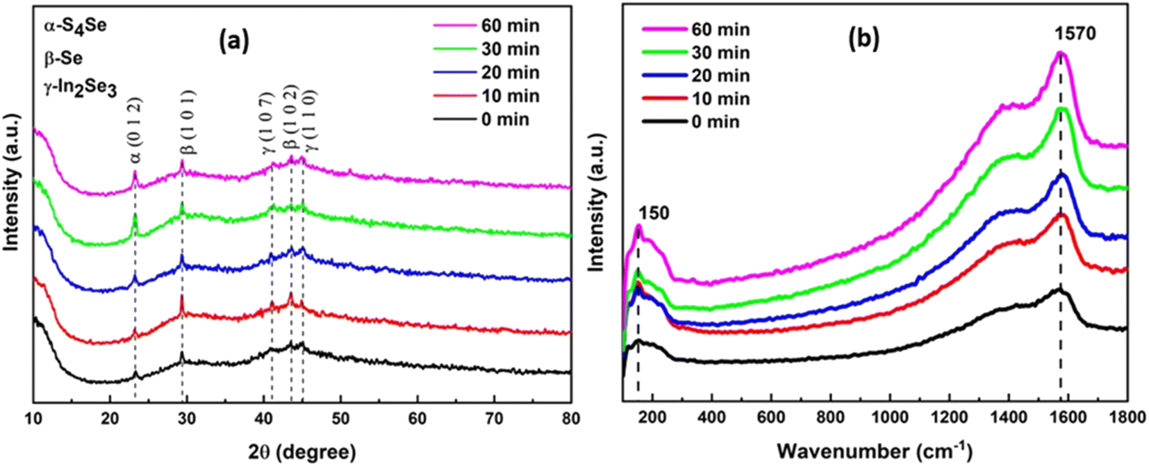
Fig. 1(a) depicts the XRD patterns of laser-irradiated Ag10In15S15Se60 films. All of the Ag10In15S15Se60 thin films exhibit polycrystalline character, according to the XRD data. Five crystalline peaks can be seen in the film that has not been exposed to laser light, indicating that crystallization can be induced during the film's deposition process. The International Center for Diffraction Data (ICDD) was matched with the observed peaks. Three distinct crystalline phases have been assigned to various diffraction peaks, including the S4Se (ICDD card: 00-047-1482) having monoclinic phase, which corresponds to the diffraction angle of 24.09°, Se (reference code: 00-001-0853) with hexagonal phase at 29.61°, 43.73° and In2Se3 (ICDD card: 00-040-1408) with hexagonal phase at 41.20° and 45.26°. With the increase of irradiation time, the peak intensity increases, that indicates the rise in their volume fraction. The fact that these peaks are more intense as the irradiation time rises indicates that the thin films are becoming highly crystalline and that the size of the crystallites is changing. Ghamdi et al. have found similar results where the sample Se75S25−xAgx crystallized after being exposed to the pulse laser.27
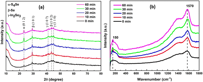 |
| | Fig. 1 (a) XRD pattern and (b) Raman spectra of Ag10In15S15Se60 laser irradiated films with different time duration. | |
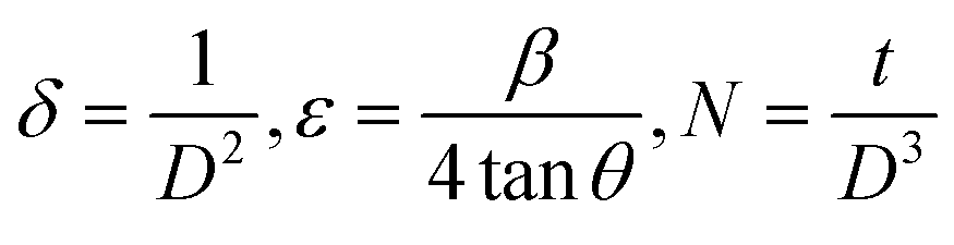
The crystallite size of the films was computed by Debye–Scherrer's formula,
| |
 | (1) |
here
k is Scherrer's constant with a value of 0.94,
β is the full width at half maximum in radians. The parameters like lattice strain (
ε), dislocation density (
δ), and number of crystallites per unit surface area (
N) are evaluated by utilizing the following formulas,
28| |
 | (2) |
All the above structural parameters are calculated, and the obtained values are shown in Table 1. The crystallite size rises, whereas the values of δ, ε, and N are reduced with the rise of laser irradiation time on In15Ag10S15Se60 thin film. It is clear that the film's crystallinity increased with the increase in irradiation time. This might be due to the recrystallization in the film that happened when the time of the laser exposure increased.29 Khudiar et al. have also reported an increase in crystallite size with the increase in laser exposure time upon the film.30
Table 1 Structural parameters of laser irradiated Ag10In15S15Se60 thin films
| Irradiation time |
D in m (× 10−8) |
δ in m−2 (× 1015) |
ε (× 10−3) |
N(1/m2) (× 1016) |
| 0 min |
1.646 |
3.690 |
8.69 |
17.937 |
| 10 min |
2.749 |
1.323 |
5.09 |
3.850 |
| 20 min |
2.813 |
1.263 |
4.9 |
3.592 |
| 30 min |
2.330 |
1.840 |
6.79 |
6.319 |
| 60 min |
2.899 |
1.189 |
5.39 |
3.281 |
3.2. Raman study
Raman spectroscopy is an essential analytical technique for examining the structural alterations in the material. Regarding the chemical bonds and atomic configurations of the material, the Raman vibrational spectra provide the necessary structural information. Fig. 1(b) shows the Raman vibrational bands at different wavenumbers. The thin film without laser irradiation shows clear bands at 150 and 1570 cm−1, whose intensity further increases with the increase of laser irradiation time. The Raman peak at 150 cm−1 can be ascribed to the B2 mode of AgInSe2 phase.31 The thin film sample exhibits the second strong Raman peak at around 1570 cm−1, corresponding to C![[double bond, length as m-dash]](https://www.rsc.org/images/entities/char_e001.gif) C stretching modes of aromatic rings.32 Further increase in the irradiation time increases the intensity of the band, and also, the surfaces of samples become rougher and more structured. As a result, the size and spacing between particles are easily changed by adjusting laser irradiation time, and the Raman signal strength can also be controlled.33
C stretching modes of aromatic rings.32 Further increase in the irradiation time increases the intensity of the band, and also, the surfaces of samples become rougher and more structured. As a result, the size and spacing between particles are easily changed by adjusting laser irradiation time, and the Raman signal strength can also be controlled.33
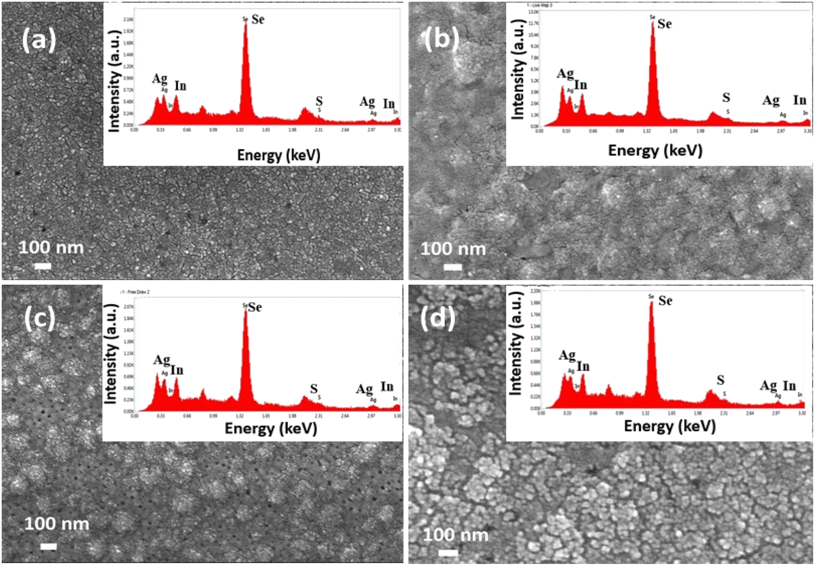
3.3. FESEM and EDX analysis
The FESEM micrographs of quaternary thin films exposed to laser radiation for 0, 10, 30, and 60 minutes are depicted in Fig. 2(a)–(d). The thin film without laser irradiation shows uniformly distributed grains throughout the image. The micrograph makes it very evident that as the irradiation time is raised, the grain size also rises, and agglomerates into various shapes. During the laser irradiation, the laser energy is transferred to the thin film resulting in the melting of the film. Then the film breaks into droplets containing solid metallic nanoparticles due to the instability of the film. But Ag has a very high melting temperature. Further, the breakup allows the self-assembly of nanoparticles to form agglomerated shapes, resulting in increased nanoparticle size with the irradiation time.33 The material's grain size increased due to the heat caused by laser irradiation. Khan et al. have observed similar changes in the surface structure of the films after laser irradiation.29 FESEM images show that the nanoparticles are formed with regulated size and consistent shape. Thus, it is possible to achieve desired size and shape by applying laser irradiation to the sample.
 |
| | Fig. 2 FESEM and EDX images of laser-irradiated Ag10In15S15Se60 thin films with irradiation time (a) 0 min (b) 10 min (c) 30 min (d) 60 min. | |
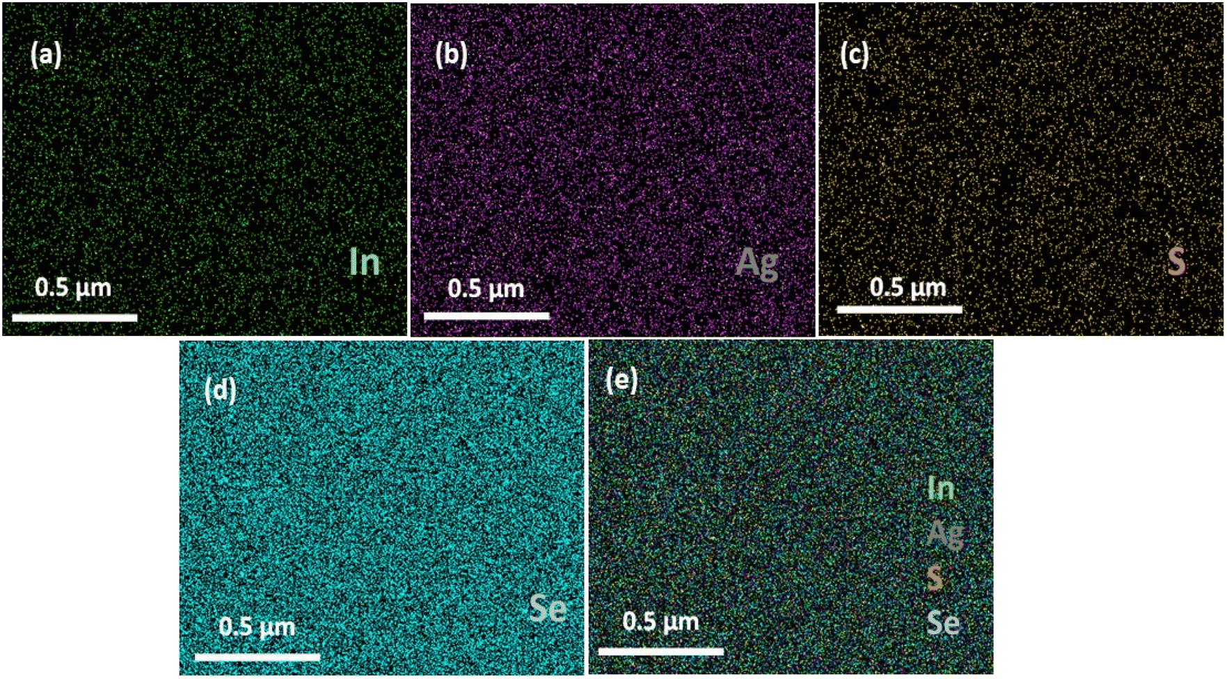
The EDX spectra are displayed with corresponding FESEM images that verified the existence of constituents elements in the Ag10In15S15Se60 thin films with regard to the respective peaks indicating the potential amount present in the sample. There is no remarkable change in composition with the irradiation time, and it is close to the starting material. All the compositional elements are present in the sample after laser irradiation which is confirmed through the EDX analysis. Similarly, Fig. 3(a)–(e), shows the elemental mapping images of the constituent elements of 60 min laser irradiated In15Ag10S15Se60 thin film.
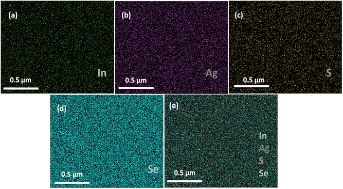 |
| | Fig. 3 Elemental mapping images of constituent elements (a) In (b) Ag (c) S (d) Se, and (e) Combined mapping image of Ag10In15S15Se60 thin film. | |
3.4. Optical analysis
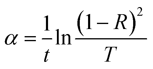
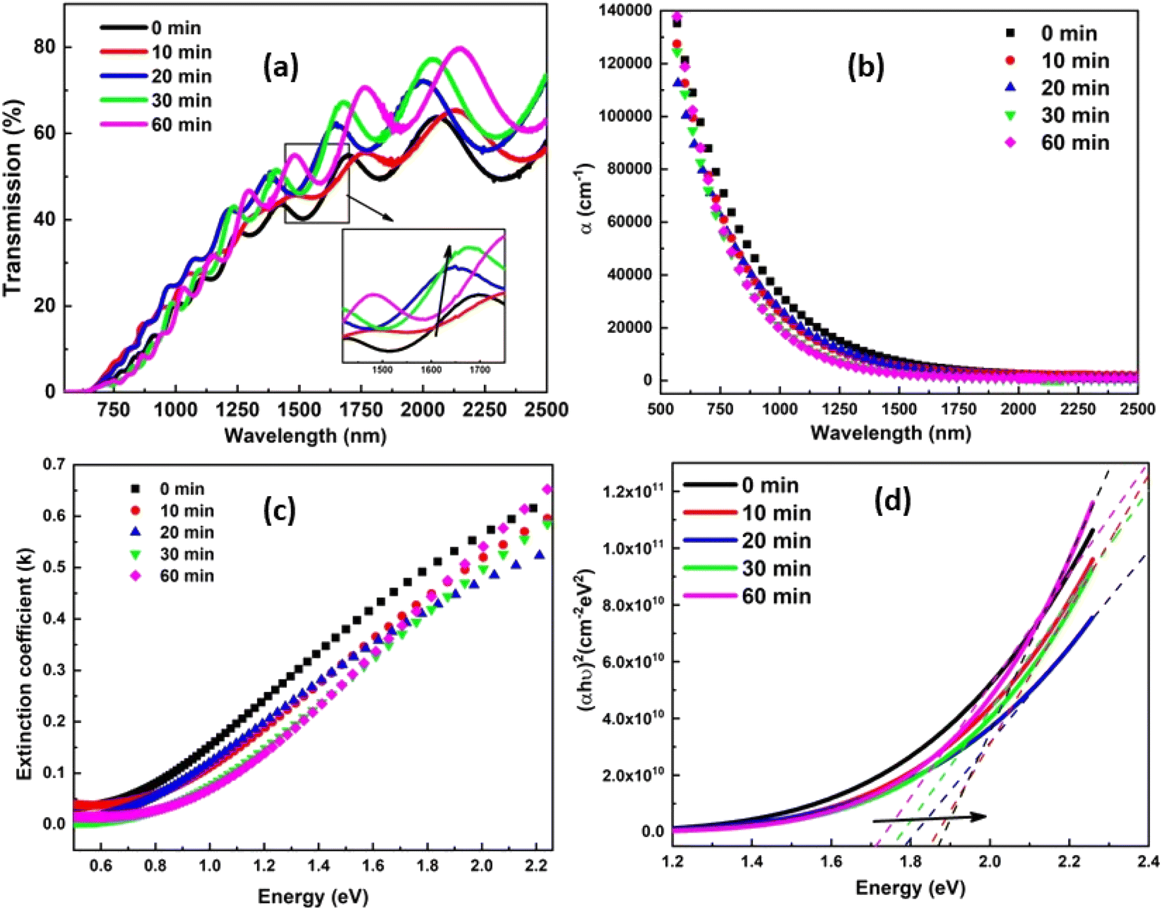
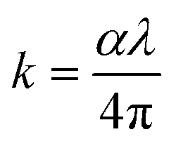
3.4.1. Transmittance, absorption coefficient, extinction coefficient, and optical bandgap. The transmittance, T, of the crystalline Ag10In15S15Se60 thin films is measured to determine their spectral dependency in the wavelength region of 600–2500 nm, as shown in Fig. 4(a). The spectra display an interference pattern for different laser irradiation times. Fig. 4(a) illustrates the fact that transmission rises as exposure time increases. The rise in crystallinity that occurs with laser irradiation time can be linked to the increase in transmittance and may result from the structure's homogenization and refilling. The absorption coefficient (α) demonstrates how effectively the films can absorb light. The value of ‘α’ for semiconductors in the strong absorption region (α ≥ 104 cm−1) is given by,34| |
 | (3) |
where ‘t’ stands for the film thickness, and ‘R’ is for their reflectance.
 |
| | Fig. 4 (a) Transmission spectra (b) absorption coefficient (c) extinction coefficient (d) calculation of optical bandgap of laser irradiated Ag10In15S15Se60 films with different time duration. | |
In the various absorption processes, both a photon and a phonon are absorbed by the electrons and holes. The required energy is provided by the photon, but the required momentum is provided by the phonon. The change in absorption coefficient (α) with energy could be understood with the help of fundamental, excitation, valence, and acceptor absorption. The absorption coefficient (α) is evaluated by using eqn (3), and the graph is shown in Fig. 4(b). From the figure, it is found that the absorption coefficient for thin film decreased with laser irradiation duration. The light intensity is reduced during the penetration in the sample due to scattering, and absorption is known as the extinction coefficient (k). The value of ‘k’ is evaluated by utilizing the absorption coefficient value in the following relation,  . The calculated value is plotted in the graph and shown in Fig. 4(c). The extinction coefficient is also decreased as the laser irradiation time increases upon the thin film surface. The k decreases with the irradiation time, which is the result of the increase in structural and surface defects caused by laser irradiation.35 The optical bandgap value (Eg) is a very important parameter that is used to select the semiconductor materials according to their applicability. Tauc suggested the direct allowed transition model, which is used to determine the optical bandgap by using Tauc's extrapolation.36
here the constant ‘
B’ is dependent on the transition probability, ‘
m’ is an index that have different values depending on the type of electronic transition that causes absorption.
37 Here the direct optical bandgap is evaluated, as the Ag
10In
15S
15Se
60 thin films showed the crystalline nature. The graph of (
αhν)
2 versus hν is shown in
Fig. 4(d). The intersection of the plot (
αhν)
2 and
hν yields the bandgap (
Eg), and the slope provides the Tauc parameter (
B2). The term ‘
B’ is highly affected by the type of bonding. The Tauc parameter rises with laser irradiation, indicating that there are more heteropolar bonds present because of chemical orderings in the film. The optical bandgap and Tauc parameter values are calculated and given in
Table 2. It was found that the bandgap values of laser-irradiated In
15Ag
10S
15Se
60 thin films increase with the increase of irradiation time, which shows the photobleaching phenomenon in the sample. Similar results showing the increase in the bandgap values after laser irradiation are also found in the reported literature.
38 The rise in bandgap might be described through the ‘density of state model’ put forward by Mott and Davis because the optical absorption is dependent on the short-range order in the amorphous states and defects linked with it.
39 In accordance with this theory, the disorderliness and defects in the amorphous structure determine the broadness of localized states around the mobility edges.
Table 2 Optical parameters of laser irradiated Ag10In15S15Se60 films with different irradiation time
| Estimated optical parameters |
0 min |
10 min |
20 min |
30 min |
60 min |
| Eg (eV) |
1.71 |
1.78 |
1.81 |
1.86 |
1.88 |
| B2 in cm−2 eV−2 |
1.85 × 10¹¹ |
1.94 × 10¹¹ |
1.69 × 10¹¹ |
2.36 × 10¹¹ |
3.07 × 10¹¹ |
| Ed (eV) |
1.46 |
1.04 |
0.70 |
0.61 |
0.48 |
| Eo (eV) |
1.466 |
1.486 |
1.481 |
1.515 |
1.535 |
| M−1 |
0.996 |
0.702 |
0.477 |
0.409 |
0.316 |
| M−3 |
0.463 |
0.317 |
0.217 |
0.178 |
0.134 |
| ε∞ |
1.996 |
1.702 |
1.477 |
1.409 |
1.316 |
| εL |
1.395 |
1.215 |
0.916 |
0.581 |
0.39 |
| f = E0Ed |
2.142 |
1.551 |
1.048 |
0.939 |
0.745 |
| N/m* |
3.78 × 10−52 |
3.28 × 10−52 |
2.49 × 10−52 |
1.77 × 10−52 |
1.15 × 10−52 |
| n0 |
1.413 |
1.304 |
1.215 |
1.187 |
1.147 |
| λ0 (nm) |
773.86 |
739.30 |
736.63 |
755.76 |
754.10 |
| S0 (nm2) |
3.62 × 10⁻⁶ |
2.89 × 10⁻⁶ |
2.27 × 10⁻⁶ |
1.56 × 10⁻⁶ |
1.16 × 10⁻⁶ |
| ηopt |
2.061 |
2.103 |
2.140 |
2.153 |
2.172 |
The variation in bandgap is also caused by the change in the position of Fermi level, which can be estimated based on how electrons are distributed among localized states.40 The irradiation time also affects the optical properties. The optical bandgap increases with the irradiation time. The presence of homopolar bonds and the dangling bonds are mainly responsible for the disorder in the sample. The irradiation process increases the structural ordering in the thin film by converting the homopolar bonds into heteropolar bonds. This finding is consistent with the fact that the latter bonds, which are stronger than the previous bonds, are more favoured as the glass strives to attain the thermal equilibrium with the lowest free energy.41 The bandgap (Eg) increases with irradiation which could be ascribed to the drop in the density of tail states near the band edge. Since the homopolar bonds are primarily responsible for the state of band tails in amorphous films, hence the enhancement in structural ordering because of the reduction in homopolar bonds results a rise in the bandgap.42
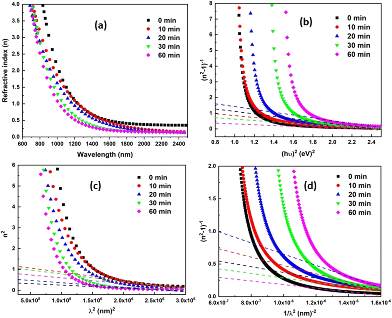
3.4.2. Refractive index, dispersive energy parameters, high-frequency dielectric constant, Sellmeier parameters. One of the crucial characteristics is the material's refractive index (n). Refractive index gives an idea about the polarization, local field, and phase velocity of light that helps to build an optical system. The refractive index is calculated by using the transmittance value by utilizing the relation as follows,43,44  . The film's refractive index decreases with laser irradiation, as shown in Fig. 5(a), which is consistent with earlier research on a variety of different high-intensity photo exposures.45,46 The ‘n’ value reduces due to the structure modification in the film, and the density of the film decrease upon exposure to light, which causes a reduction in the refractive index value.47 As stated by Moss's rule (Egn4 ∼ constant), the drop in the refractive index is typically followed by a rise in the bandgap.48 The decreasing behaviour of ‘n’ with regard to wavelength represents typical dispersion behaviour. The Wemple–DiDomenico (WDD) single oscillator model is used to study the refractive index dispersion. The dispersion parameters are evaluated by using the following relations,49,50
| |
 | (5) |
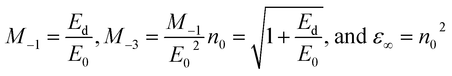
where ‘E0’ and ‘Ed’ denotes the oscillator and dispersion energy. ‘Ed’ indicates the strength in which the optical transitions occurred among two optical bands. Fig. 5(b) shows the graph of (n2 − 1)−1 vs. (hν)2 drawn with the help of eqn (7). The value of the Ed, E0 are evaluated from the intercept and slope of the plot. The E0 value also referred to as the average energy gap, offers exact details about the sample's complete band structure. The ‘Ed’ is related to the physical properties of the material and is connected to the alteration in the sample's structural ordering. The increase of Ed is frequently regarded as a microstructural order parameter since it is associated with the development of the thin film microstructure into a more ordered phase. For the present sample, the value of dispersion energy decreases with laser irradiation time. This shows that the irradiated film has less structural order than the without irradiation film. This local microstructural ordering may have a significant impact on the film density, which may result in the reduction of the refractive index of irradiated films. It is noted that the Ed decreased with irradiation time, whereas the value of E0 exhibits the reverse manner of Ed. As a result of local structure modification in the film, the film's density decreases upon laser irradiation, which causes a reduction in the refractive index.46 The increase in irradiation time results in the photobleaching phenomenon accompanied by a shift of transmission edge to a lower wavelength. This corresponding increase in E0 values shifts the absorption edge toward higher energy resulting the increase in bandgap as well as the decrease in the refractive index. The oscillator strength (f) of the film could be calculated by multiplying the E0 and Ed values (f = E0Ed).51 From Table 2, the computed values of ‘f’ show a decreasing order with the irradiation time. Furthermore, the dispersion parameters are used to calculate the first-order moments (M−1), third-order moments (M−3), dielectric constant (ε∞), and static refractive index (n0) using the following relations,52| |
 | (6) |
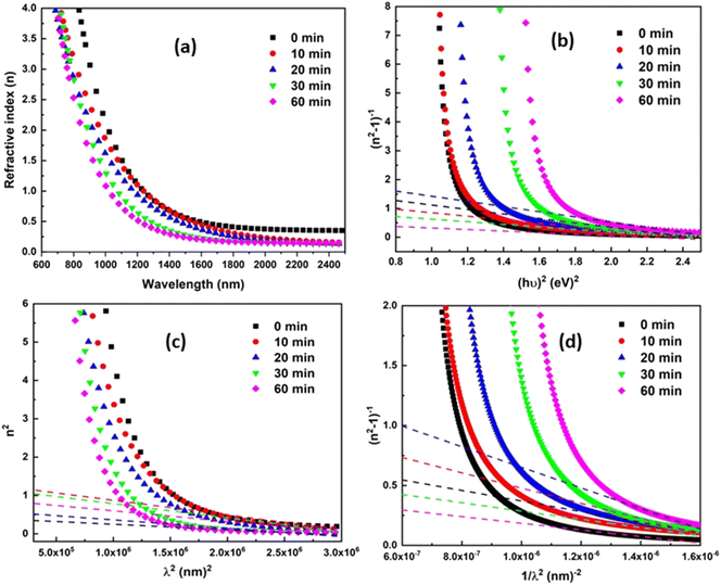 |
| | Fig. 5 (a) Variation of ‘n’ with ‘λ’ (b) variation of (n2 − 1)−1 vs. hν (c) variation of n2 vs. λ2 (d) change of (n2 − 1)−1 vs. 1/λ2 laser irradiated Ag10In15S15Se60 films with different time duration. | |
All the calculated values from the above relations are tabulated in Table 2. The value of ‘n0’ reduced along the irradiation time, which agrees with the linear refractive index. The parameters like high-frequency dielectric constant (εL) and the carrier concentration per unit mass (N/m*) can also be evaluated by using the relation,53
| |
 | (7) |
here ‘
C’ stands for the speed of light in a vacuum, and ‘
e’ stands for an electronic charge. The intercept and slope of
n2 vs. λ2 graph are used to calculate the
εL and
N/
m*, shown in
Fig. 5(c). These values are produced by considering the free-electron charge carriers and lattice vibrational modes of the system. With laser irradiation, the
εL values show a declining pattern of behaviour. The obtained results complement the encouraging values of optical nonlinearity because both
εL and
N/
m* contribute to the polarization of the material.
54
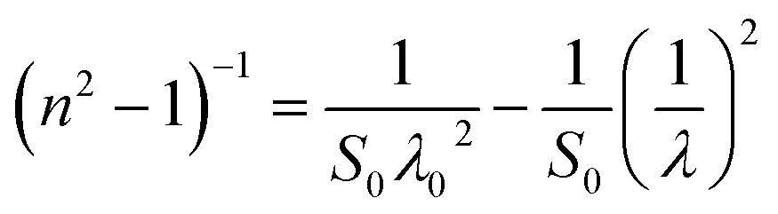
Sellmeier proposed a classical dispersion relation at low frequency for refractive index based on the single oscillator model is stated as,55
| |
 | (8) |
where
S0 and
λ0 represent oscillator strength and oscillator wavelength, respectively. Using
eqn (10), the graph plotted between (
n2 − 1)
−1 and 1/
λ2 from which the slope and the intercept value are used to calculate
S0 and
λ0 values. From
Table 2, it is found that both
S0 and
λ0 values decreased with the irradiation time. The observed results from both dispersion models suggest that the investigated dispersion behaviour of the film favours the development of photonic applications since it exhibits noticeable alteration when exposed to laser light.
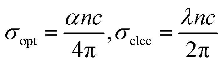
3.4.3. Optical density, optical, and electrical conductivity. The optical density (OD) of the materials is a measure of how well they can absorb electromagnetic radiation. The formula OD = α × t is used to get the OD value.56 According to Fig. 6(a), the optical density varies with wavelength and decreases over the course of irradiation time. The decreasing behaviour of the OD is because of the reduction in the α value. The optical and electrical conductivity of the material can provide detailed knowledge about the electronic states, and those could be determined by using the value of α, n, and λ in the relation,57
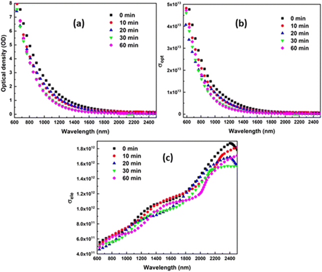 |
| | Fig. 6 Variation of (a) OD with wavelength (b) optical conductivity, and (c) electrical conductivity with the wavelength of laser irradiated Ag10In15S15Se60 films with different time duration. | |
The conductance of charge carriers because of optical excitation is represented by the σopt. Fig. 6(b) and (c) shows the fluctuation of these two conductivities (σopt and σele) at various irradiation times. Both the conductivities decreased with the irradiation time, that is because of loss in ‘α’ and density of localized defect states caused by the irradiation.58
3.4.4. Real dielectric constant (εr), imaginary dielectric constant (εi), and dielectric loss factor. The dielectric properties of the material greatly influence the polarizability of the material. The polarizability of the material is very important and suitable for different photonics applications. The complex dielectric constant contains two parts a real part and an imaginary part. The relation is given as ε* = εr + iεi = (n + ik)2, where εr and εi represent real and imaginary dielectric constants. The value of both εr and εi is evaluated by using the given equations,59
| εr = n2 − k2 and εi = 2nk |
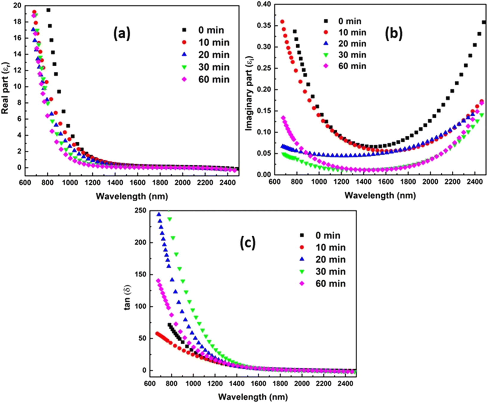
The imaginary portion (εi) indicates the energy from the electric field that is absorbed by dipole motion and describes the disruptive rate of the wave of the sample. The real part (εr) denotes the dispersion of electromagnetic waves moving inside the sample and also signifies the deduction in its propagation speed.60 Fig. 7(a) and (b) show how the εr and εi behave with wavelength over various time domains of laser irradiation. It is evident that the values of εr > εi, that is because of the dependence of εr on higher ‘n’ values as compared to lower values of ‘k’. The change in the dielectric properties with the change in wavelength indicates a possible interaction among photons and free electrons. The behavioural change in dielectric properties during laser irradiation suggests a reduction in the amount of energy lost and the disruptive rate of electromagnetic waves.61
 |
| | Fig. 7 (a) Variation of εr vs. λ (b) plot of εi vs. λ, and (c) variation of dielectric loss factor of the film with different irradiation time. | |
Furthermore, the relationship between the εr and εi can be utilized to determine the medium's dielectric loss, tan(δ) = εi/εr, where ‘δ’ represents the loss angle. The loss factor provides the loss rate of mechanical mode power of a dissipative medium.11 Fig. 7(c) shows the rise in dielectric loss of the system with the rise of laser exposure time on film, whereas, for 60 minutes of irradiation time, the energy loss again decreases.
The electron losses its energy when traveling in the material, which could be divided into two parts volume energy loss function (VELF) and surface energy loss function (SELF). Both parameters are calculated by given relations,62
| |
 | (9) |
Fig. 8(a) and (b) show the change of VELF and SELF with wavelength at different irradiation times. From the figure, it is observed that the volume energy losses increased, whereas the surface energy losses decreased with the rise of irradiation time. The increase in losses can be referred to as the increase in the optical path inside the semiconductor.
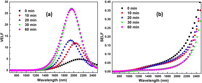 |
| | Fig. 8 Variation of (a) VELF with wavelength (b) SELF with the wavelength of laser irradiated Ag10In15S15Se60 films. | |
The parameter optical electronegativity defines the tendency of atoms and molecules to make ionic bonds because of their attractive nature towards electrons. Duffy proposes the relation to calculate the value of optical electronegativity as,
where ‘
C’ represents a constant value of 25.54. The calculated values are presented in
Table 2 and were found in increasing order with the irradiation time.
3.5. Nonlinear optical parameters
The nonlinear relationship among optical characteristics and the material's electric field is referred to as optical nonlinearity. The nonlinear properties have a large importance in the field of nonlinear devices such as all-optical switching and integrated photonic devices etc.63 When intense light is exposed to the material, polarization develops, and hence nonlinearity appears because of the nuclear interaction with electronic polarizability (αp), that further influences the bond length.64 The dipole moment and the susceptibility (χ) are directly proportional, which can be represented as P = ε0χE, where ε0 and E represent the permeability of free space and electric field intensity, respectively. The susceptibility contributes to both the linear as well as nonlinear portions: χ = χL + χNL. The linear part contains χL = χ(1), whereas the nonlinear part of the susceptibility contains χNL = χ(2) + χ(3). The first-order and third-order nonlinear susceptibility (χ(1), χ(3)) are determined by utilizing the relation given as,65,66| |
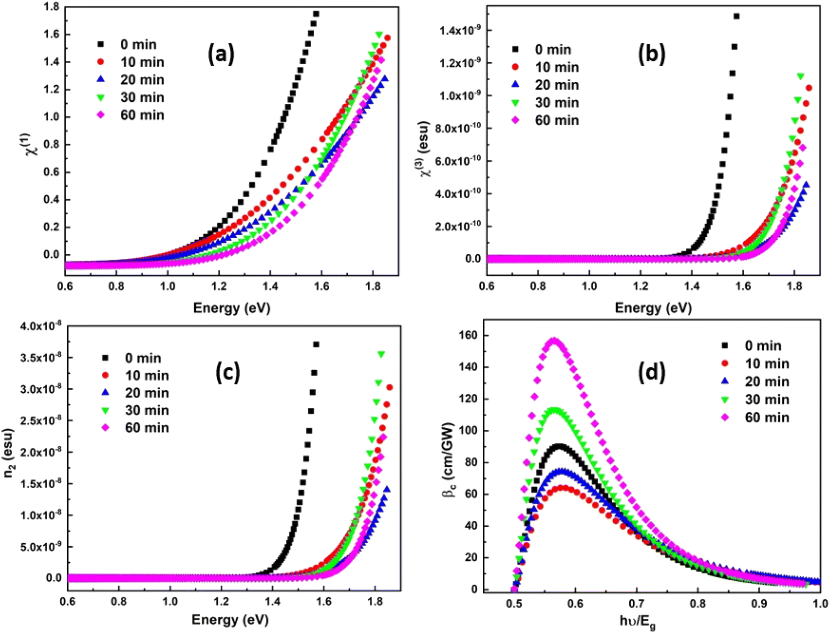
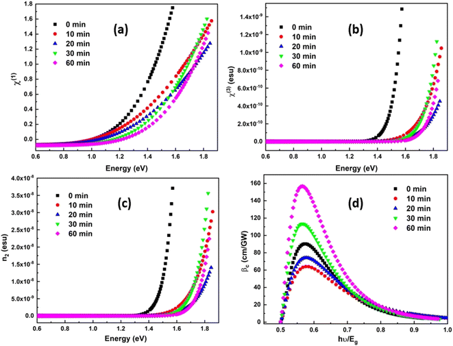
 | (10) |
where ‘A’ has the value of 1.7 × 10⁻¹⁰ esu. The first-order and second-order optical nonlinearities values are drawn with energy values shown in Fig. 9(a) and (b). It is observed that both the values of χ(1) and χ(3) decreased with the increase in irradiation time. Furthermore, the nonlinear refractive index (n2) is calculated from Ticha and Tichy's relation67  , where n0 represents the static refractive index at hν → 0. Fig. 9(c) shows the variation of nonlinear refractive index with energy. It is found that the n2 value decreases with the rise of irradiation time. The decrease in nonlinear parameters due to irradiation is also reported in other studies.47 The decrease in n2 and χ(3) is due to the decrease in Ed/E0 ratio. The variation in the n2 and χ(3) parameters are beneficial in UV nonlinear optical material, solid-state laser.68
 |
| | Fig. 9 (a) Variation of χ(1) with energy for different irradiation time (b) plot for χ(3) vs. energy (c) variation of n2 with energy (d) variation of βc with hν/Eg for different irradiation time. | |
The two-photon absorption phenomenon is a well-known characteristic of chalcogenide materials. The interaction of light with semiconductor material with high optical nonlinearity leads to a multiphoton process. This makes semiconductor materials like chalcogenides as potential candidates for various photonics devices. In this nonlinear phenomenon, an electron is simultaneously stimulated from its ground state to higher states, and two or more photons are absorbed.69 Thus the nonlinear absorption coefficient (βc) can be defined as the efficiency of two-photon absorption in semiconductor materials which further depends on optical bandgap (Eg) and photon energy (hν). The nonlinear absorption coefficient is calculated by using the following relation,70
| |
 | (11) |
Fig. 9(d) shows the variation of βc with hν/Eg. From the figure, it is found that the overall non-linear absorption coefficient increases with the rise of irradiation time on the thin film.
4. Conclusion
The quaternary thin films prepared by the thermal evaporation method is exposed to laser light for different time durations, and the relative changes in the linear and nonlinear optical parameters are investigated. The XRD spectra confirmed the polycrystalline nature of the film, and also the obtained crystallite size increased with the rise of irradiation time. The average crystallite size increased whereas the dislocation density decreased with irradiation time. The change in the morphology is clearly distinguished from the FESEM images as the roughness of the films increased with irradiation time. The transmission increased, whereas the absorption coefficient, extinction coefficient, and optical density decreased with the irradiation time. The shift absorption edge towards lower wavelength leads to the increase of bandgap and hence the decrease of refractive index with the irradiation time. The oscillator energy increased whereas the dispersion energy decreased with irradiation time. The real and imaginary dielectric constants are found to be decreased with irradiation. The increase in optical electronegativity also led to the variation in nonlinear optical properties due to the presence of extra lone pairs. The nonlinear absorption coefficient increased with laser irradiation. The nonlinear susceptibility, as well as the nonlinear refractive index, decreased with the irradiation time. These films are strong contenders for optoelectronic applications because of their linear and nonlinear optical responses.
Author contributions
Abinash Parida: writing – original draft, software, data curation, investigation. D. Alagarasan: investigation, experiments. R. Ganesan: visualization, investigation. Sagar Bisoyi: experiments, investigation. R. Naik: conceptualization, methodology, writing – review & editing, Supervision.
Conflicts of interest
The authors declare that they have no known competing financial interests or personal relationships that could have appeared to influence the work reported in this paper.
Acknowledgements
Dr Naik thanks IISc Bangalore for optical measurements.
References
- A. H. Ammar, A. A. M. Farag and M. S. Abo-Ghazala, Influence of Sb addition on the structural and optical characteristics of thermally vacuum evaporated SbxSe1−x thin films, J. Alloys Compd., 2017, 694, 752–760 CrossRef CAS.
- A. M. Adam, E. Lilov, V. Lilova and P. Petkov, Characterization and optical properties of bismuth chalcogenide films prepared by pulsed laser deposition technique, Mater. Sci. Semicond. Process., 2017, 57, 210–219 CrossRef CAS.
- M. M. El-Nahass, A. A. Attia, H. A. M. Ali, G. F. Salem and M. I. Ismail, Nature of electrical transport properties of nanocrystalline ZnIn2Se4 thin films, Chaos, Solitons Fractals, 2017, 95, 52–56 CrossRef.
- P. Kumar and R. Thangaraj, Effect of phase separation on the kinetics of photocurrent relaxation in Sn–Sb–Se glassy films, J. Phys.: Condens. Matter, 2009, 21, 375102 CrossRef PubMed.
- S. Shukla and S. Kumar, Role of Sb incorporation on the electrical and photoelectrical properties of Se-In glassy alloy, J. Non-Cryst. Solids, 2011, 357, 847–850 CrossRef CAS.
- A. K. Diab, M. M. Wakkad, E. K. Shokr and W. S. Mohamed, Structural and electrical properties of In35Sb45Se20−xTex chalcogenide thin films, Optik, 2015, 126, 1855–1860 CrossRef CAS.
- V. Kumari, A. Kaswan, D. Patidar, K. Sharma and N. S. Saxena, Electrical conduction mechanism in GeSeSb chalcogenide glasses, Bull. Mater. Sci., 2016, 39, 255–262 CrossRef CAS.
- A. S. Krymus, G. L. Myronchuk, O. V. Parasyuk, G. Lakshminarayana, A. O. Fedorchuk, A. El-Naggar, A. Albassam and I. V. Kityk, Photoconductivity and nonlinear optical features of novel AgxGaxGe1-xSe2 crystals, Mater. Res. Bull., 2017, 85, 74–79 CrossRef CAS.
- K. S. Bindra, N. Suri, P. Kumar and R. Thangaraj, Effect of Ag addition on the photoconductivity of amorphous Se–Sb thin films, Solid State Commun., 2007, 144, 83–87 CrossRef CAS.
- L. Jatautė, V. Krylova, N. Dukštienė, M. Lelis and S. Tučkutė, Ag-In-Se films on flexible architectural textiles as efficient material for optoelectronics applications: A preliminary study, Thin Solid Films, 2021, 721, 138566 CrossRef.
- S. Mishra, P. Kumar Singh, R. K. Yadav, A. Umar, P. Lohia and D. K. Dwivedi, Investigation of glass forming ability, linear and non-linear optical properties of Ge-Se-Te-Sb thin films, Chem. Phys., 2021, 541, 111021 CrossRef CAS.
- M. Pandian, P. Matheswaran, B. Gokul, R. Sathyamoorthy and K. Asokan, Preparation and characterization of indium chalcogenide thin films: a material for phase change memory, Appl. Surf. Sci., 2018, 449, 55–67 CrossRef CAS.
- P. Singh, P. Sharma, V. Sharma and A. Thakur, Linear and non-linear optical properties of Ag-doped Ge2Sb2Te5 thin films estimated by single transmission spectra, Semicond. Sci. Technol., 2017, 32, 045015 CrossRef.
- L. Tian, H. I. Elim, W. Ji and J. J. Vittal, One-pot synthesis and third-order nonlinear optical properties of AgInS2 nanocrystals, Chem. Commun., 2006, 4276–4278 RSC.
- R. Naik, C. Sripan and R. Ganesan, Photo darkening in As50Se50 thin films by 532 nm laser irradiation, Opt. Laser Technol., 2017, 90, 158–164 CrossRef CAS.
- K. Tanaka, Photo-induced phenomena in chalcogenide glass: Comparison with those in oxide glass and polymer, J. Non-Cryst. Solids, 2006, 352, 2580–2584 CrossRef CAS.
- P. Fabbri and M. Messori, Surface modification of polymers: chemical, physical, and biological routes, Modification of Polymer Properties, 2017, vol. 352, pp. 109–130 Search PubMed.
- B. J. Eggleton, B. Luther-Davies and K. Richardson, Chalcogenide photonics, Nat. Photonics, 2011, 535, 141–148 CrossRef.
- T. Robinson, S. O. Kasap, A. C. van Popta, C. J. Haugen, J. N. McMullin, R. G. DeCorby and D. Tonchev, Photoinduced refractive index change in As2Se3 by 633nm illumination, Opt. Express, 2002, 10, 639–644 CrossRef PubMed.
- P. Pradhan, R. Naik, N. Das and A. K. Panda, Band gap tuning in As40Se53Sb07 thin films by 532 nm laser irradiation: An optical investigation by spectroscopic techniques, Opt. Mater., 2018, 75, 699–709 CrossRef CAS.
- Y. Ikeda and K. Shimakawa, In situ simultaneous measurements of photodarkening and photoinduced volume changes in chalcogenide glasses, J. Non-Cryst. Solids, 2006, 352, 1582–1586 CrossRef CAS.
- S. Zhang, Y. Chen, R. Wang, X. Shen and S. Dai, Observation of photobleaching in Ge-deficient Ge16.8Se83.2 chalcogenide thin film with prolonged irradiation, Sci. Rep., 2017, 7, 1–7 CrossRef PubMed.
- V. Lyubin, M. Klebanov, A. Bruner, N. Shitrit and B. Sfez, Transient photodarkening and photobleaching in glassy GeSe2 films, Opt. Mater., 2011, 33, 949–952 CrossRef CAS.
- C. Y. Yan, B. A. Liu, X. C. Li, C. Liu and X. Ju, Time-dependent photothermal characterization on damage of fused silica induced by pulsed 355-nm laser with high repetition rate, Chin. Phys. B, 2020, 29, 027901 CrossRef CAS.
- R. Naik, S. Jena, R. Ganesan and N. K. Sahoo, Photo-induced optical bleaching in Ge12Sb25S63 amorphous chalcogenide thin films: effect of 532 nm laser illumination, Laser Phys., 2015, 25, 036001 CrossRef.
- A. Parida, D. Sahoo, D. Alagarasan, S. Varadhrajaperumal, R. Ganesan and R. Naik, Impact on Nonlinear/Linear optical and structural parameters in quaternary In15Ag10S15Se60 thin films upon annealing at different temperatures, Ceram. Int., 2022, 48, 15380–15389 CrossRef CAS.
- A. A. Al-Ghamdi and S. A. Khan, Laser-induced changes on optical band gap of amorphous and crystallized thin films of Se75S25−xAgx, Phys. B, 2009, 404, 4262–4266 CrossRef CAS.
- P. Priyadarshini, S. Das, D. Alagarasan, R. Ganesan, S. Vardharajperumal and R. Naik, Observation of high nonlinearity in Bi doped BixIn35-xSe65 thin films with annealing, Sci. Rep., 2021, 11, 21518 CrossRef CAS PubMed.
- M. I. Khan and A. Ali, Effect of laser irradiation on the structural, morphological and electrical properties of polycrystalline TiO2 thin films, Results Phys., 2017, 7, 3455–3458 CrossRef.
- A. I. Khudiar, M. Zulfequar and Z. H. Khan, Laser wavelength effect on structural and optical properties of Cd34Se66 nanocrystalline thin film, J. Non-Cryst. Solids, 2011, 357, 1264–1269 CrossRef CAS.
- Y. Jin, K. Tang, C. An and L. Huang, Hydrothermal synthesis and characterization of AgInSe2 nanorods, J. Cryst. Growth, 2003, 253, 429–434 CrossRef CAS.
- J. C. Valmalette, Z. Tan, H. Abe and S. Ohara, Raman scattering of linear chains of strongly coupled Ag nanoparticles on SWCNTs, Sci. Rep., 2014, 4, 1–8 Search PubMed.
- R. Hong, W. Shao, W. Sun, C. Deng, C. Tao and D. Zhang, Laser irradiation induced tunable localized surface plasmon resonance of silver thin film, Opt. Mater., 2018, 77, 198–203 CrossRef CAS.
- A. Parida, D. Sahoo, D. Alagarasan, S. Varadhrajaperumal, R. Ganesan and R. Naik, Enhancing the third-order nonlinearity and crystallinity by selenium incorporation in tin sulfide films (SnS1−x Sex) for optoelectronic applications, Mater. Adv., 2022, 3, 5930–5940 RSC.
- M. Jin, P. Chen, P. Boolchand, T. Rajagopalan, K. L. Chopra, K. Starbova and N. Starbov, Origin of giant photocontraction in obliquely deposited amorphous GexSe1-x thin films and the intermediate phase, Phys. Rev. B: Condens. Matter Mater. Phys., 2008, 78, 214201 CrossRef.
- J. Tauc, Amorphous and liquid semiconductors, Plenum Press, New York, 1979, p. 159 Search PubMed.
- S. Das, D. Alagarasan, S. Vardharajaperumal, R. Ganesan and R. Naik, Tuning the nonlinear susceptibility and linear parameters upon annealing the Ag60-xSe40Tex nanostructured films for nonlinear and photonic applications, Mater. Adv., 2022, 3, 7640–7654 RSC.
- R. Naik, S. Jena, R. Ganesan and N. K. Sahoo, Effect of laser irradiation on optical properties of Ge12Sb25Se63 amorphous chalcogenide thin films, Indian J. Phys., 2015, 89, 1031–1040 CrossRef CAS.
- Y. H. Wang, J. Lin and C. H. A. Huan, Structural and optical properties of a-Si:H/nc-Si:H thin films grown from Ar–H2–SiH4 mixture by plasma-enhanced chemical vapor deposition, Mater. Sci. Eng., B, 2003, 104, 80–87 CrossRef.
- A. Kumara and P. K. Ahluwalia, Electronic structure of transition metal dichalcogenides monolayers 1H-MX2 (M = Mo, W; X = S, Se, Te) from ab-initio theory: new direct band gap semiconductors, Eur. Phys. J. B, 2012, 85, 1–7 CrossRef.
- Q. Yan, H. Jain, J. Ren, D. Zhao and G. Chen, Effect of photo-oxidation on photobleaching of GeSe2 and Ge2Se3 films, J. Phys. Chem. C, 2011, 115, 21390–21395 CrossRef CAS.
- W. H. Wei, S. Xiang, S. W. Xu, L. Fang and R. P. Wang, Structural investigation on GexSb10Se90−x glasses using x-ray photoelectron spectra, J. Appl. Phys., 2014, 115, 183506 CrossRef.
- S. Yaseem, F. Iqbal, T. Munawar, M. A. Nawaz, M. Asghar and A. Hussain, Synthesis, structural and optical analysis of surfactant assisted ZnO–NiO nanocomposites prepared by homogeneous precipitation method, Ceram. Int., 2019, 45, 17859–17873 CrossRef.
- S. Das, P. Priyadarshini, D. Alagarasan, R. Ganesan, S. Vardharajperumal and R. Naik, Structural, morphological, and linear/non-linear optical properties tuning in Ag60-xSe40Tex films by thermal annealing for optoelectronics, J. Non-Cryst. Solids, 2022, 592, 121742 CrossRef CAS.
- S. K. Tripathi, S. Gupta, F. I. Mustafa, N. Goyal and G. S. S. Saini, Laser induced changes on a-Ga50Se50 thin films, J. Phys. D: Appl. Phys., 2009, 42, 185404 CrossRef.
- X. Su, R. Wang, B. Luther-Davies and L. Wang, The dependence of photosensitivity on composition for thin films of GexAsySe1-x-y chalcogenide glasses, Appl. Phys. A: Mater. Sci. Process., 2013, 113, 575–581 CrossRef CAS.
- A. V. Kolobov, Photo-induced metastability in amorphous semiconductors, 2003, p. 412 Search PubMed.
- P. Knotek, L. Tichy, D. Arsova, Z. G. Ivanova and H. Ticha, Irreversible photobleaching, photorefraction and photoexpansion in GeS2 amorphous film, Mater. Chem. Phys., 2010, 119, 315–318 CrossRef CAS.
- I. M. El Radaf, H. Y. S. Al-Zahrani and A. S. Hassanien, Novel synthesis, structural, linear and nonlinear optical properties of p-type kesterite nanosized Cu2MnGeS4 thin films, J. Mater. Sci.: Mater. Electron., 2020, 31, 8336–8348 CrossRef CAS.
- S. H. Wemple and M. DiDomenico, Behavior of the electronic dielectric constant in covalent and ionic materials, Phys. Rev. B: Solid State, 1971, 3, 1338 CrossRef.
- A. S. Hassanien, Studies on dielectric properties, opto-electrical parameters and electronic polarizability of thermally evaporated amorphous Cd50S50−xSex thin films, J. Alloys Compd., 2016, 671, 566–578 CrossRef CAS.
- A. S. Hassanien, R. Neffati and K. A. Aly, Impact of Cd-addition upon optical properties and dispersion parameters of thermally evaporated CdxZn1-xSe films: discussions on bandgap engineering, conduction, and valence band positions, Optik, 2020, 212, 164681 CrossRef CAS.
- M. M. El-Nahass, M. H. Ali and I. T. Zedan, Photoinduced changes in the linear and non-linear optical properties of Ge10In10Se80 thin films, J. Non-Cryst. Solids, 2014, 404, 78–83 CrossRef CAS.
- D. Sahoo, P. Priyadarshini, R. Dandela, D. Alagarasan, R. Ganesan, S. Varadharajaperumal and R. Naik, In situ laser irradiation: the kinetics of the changes in the nonlinear/linear optical parameters of As50Se40Sb10 thin films for photonic applications, RSC Adv., 2021, 11, 16015–16025 RSC.
- F. Yakuphanoglu, A. Cukurovali and I. Yilmaz, Determination and analysis of the dispersive optical constants of some organic thin films, Phys. B, 2004, 351, 53–58 CrossRef CAS.
- F. A. Al-Agel, S. A. Khan, E. A. Al-Arfaj, F. M. Al-Marzouki, A. A. Al-Ghamdi, Z. H. Khan and M. Zulfequar, Influence of laser-irradiation on structural and optical properties of phase change Ga25Se75−xTex thin films, Mater. Lett., 2013, 92, 424–426 CrossRef CAS.
- M. M. Soraya, Structural and optical properties of Se85−xTe15Inx chalcogenide thin films for optoelectronics, Appl. Phys. A: Mater. Sci. Process., 2020, 126, 1–9 CrossRef.
- F. Yakuphanoglu, A. Cukurovali and I. Yilmaz, Refractive index and optical absorption properties of the complexes of a cyclobutane containing thiazolyl hydrazone ligand, Opt. Mater., 2005, 27, 1363–1368 CrossRef CAS.
- P. Priyadarshini, D. Alagarasan, R. Ganesan, S. Varadharajaperumal and R. Naik, Influence of proton ion irradiation on the linear–nonlinear optoelectronic properties of Sb40Se20S40 thin films at different fluences for photonic devices, ACS Appl. Opt. Mater., 2023, 1(1), 55–68 CrossRef.
- S. Ikeda and M. Aniya, Correlation between the nonlinear optical constants and the structural relaxation parameters in chalcogenide glasses, J. Non-Cryst. Solids, 2012, 358, 2381–2384 CrossRef CAS.
- Q. Shen, K. Katayama, T. Sawada and T. Toyoda, Characterization of electron transfer from CdSe quantum dots to nanostructured TiO2 electrode using a near-field heterodyne transient grating technique, Thin Solid Films, 2008, 516, 5927–5930 CrossRef CAS.
- M. S. El-Bana and S. S. Fouad, Optoelectrical properties of Ge10Se90 and Ge10Se85Cu5 thin films illuminated by laser beams, Appl. Phys. A: Mater. Sci. Process., 2018, 124, 1–8 CrossRef CAS.
- Q. Liu and X. Zhao, Non-linear optical properties of chalcogenide and chalcohalide glasses, J. Non-Cryst. Solids, 2010, 356, 2375–2377 CrossRef CAS.
- L. K. Benjamin, P. Dube, C. B. Tabi and C. M. Muiva, Physical, linear and nonlinear optical properties of amorphous Se90-xTe10Mx (M = Zn, In, Pb, x = 0, 5) chalcogenide thin films by electron-beam deposition, J. Non-Cryst. Solids, 2021, 557, 120646 CrossRef CAS.
- H. Ticha, L. Tichy and L. Tichy, Semiempirical relation between non-linear susceptibility (refractive index), linear refractive index and optical gap and its application to amorphous chalcogenides, J. Optoelectron. Adv. Mater., 2002, 4, 381–386 CAS.
- R. Chauhan, A. K. Srivastava, A. Tripathi and K. K. Srivastava, Linear and nonlinear optical changes in amorphous As2Se3 thin film upon UV exposure, Prog. Nat. Sci.: Mater. Int., 2011, 21, 205–210 CrossRef.
- L. Tichý, H. Ticha, P. Nagels, R. Callaerts, R. Mertens and M. Vlček, Optical properties of amorphous As-Se and Ge-As-Se thin films, Mater. Lett., 1999, 39, 122–128 CrossRef.
- X. Dong, L. Huang, Q. Liu, H. Zeng, Z. Lin, D. Xu and G. Zou, Perfect balance harmony in Ba2NO3(OH)3 : a beryllium-free nitrate as a UV nonlinear optical material, Chem. Commun., 2018, 54, 5792–5795 RSC.
- M. Dongol, A. F. Elhady, M. S. Ebied and A. A. Abuelwafa, Effect of Thermal Annealing on the Optical Properties of Ge20Se65S15 Thin Films, Indian J. Phys., 2021, 95, 1245–1253 CrossRef CAS.
- A. A. Abuelwafa, M. S. A. El-sadek, S. Elnobi and T. Soga, Effect of Transparent Conducting Substrates on the Structure and Optical Properties of Tin (II) Oxide (SnO) Thin Films: Comparative Study, Ceram. Int., 2021, 47, 13510–13518 CrossRef CAS.
|
| This journal is © The Royal Society of Chemistry 2023 |
Click here to see how this site uses Cookies. View our privacy policy here. 
 Open Access Article
 This Open Access Article is licensed under a Creative Commons Attribution-Non Commercial 3.0 Unported Licence
 *a
*a
 . The calculated value is plotted in the graph and shown in Fig. 4(c). The extinction coefficient is also decreased as the laser irradiation time increases upon the thin film surface. The k decreases with the irradiation time, which is the result of the increase in structural and surface defects caused by laser irradiation.35 The optical bandgap value (Eg) is a very important parameter that is used to select the semiconductor materials according to their applicability. Tauc suggested the direct allowed transition model, which is used to determine the optical bandgap by using Tauc's extrapolation.36
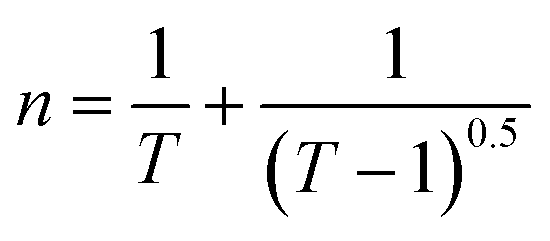 . The film's refractive index decreases with laser irradiation, as shown in Fig. 5(a), which is consistent with earlier research on a variety of different high-intensity photo exposures.45,46 The ‘n’ value reduces due to the structure modification in the film, and the density of the film decrease upon exposure to light, which causes a reduction in the refractive index value.47 As stated by Moss's rule (Egn4 ∼ constant), the drop in the refractive index is typically followed by a rise in the bandgap.48 The decreasing behaviour of ‘n’ with regard to wavelength represents typical dispersion behaviour. The Wemple–DiDomenico (WDD) single oscillator model is used to study the refractive index dispersion. The dispersion parameters are evaluated by using the following relations,49,50
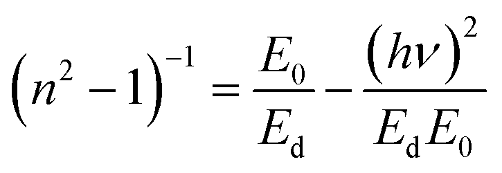


 , where n0 represents the static refractive index at hν → 0. Fig. 9(c) shows the variation of nonlinear refractive index with energy. It is found that the n2 value decreases with the rise of irradiation time. The decrease in nonlinear parameters due to irradiation is also reported in other studies.47 The decrease in n2 and χ(3) is due to the decrease in Ed/E0 ratio. The variation in the n2 and χ(3) parameters are beneficial in UV nonlinear optical material, solid-state laser.68