
 Open Access Article
 This Open Access Article is licensed under a Creative Commons Attribution-Non Commercial 3.0 Unported Licence
Interface contact and modulated electronic properties by in-plain strains in a graphene–MoS2 heterostructure†
Qian Wang a,
Zhenjun Songb,
Junhui Taoa,
Haiqin Jina,
Sha Lia,
Yuran Wanga,
Xuejuan Liuc and
Lin Zhang*a
a,
Zhenjun Songb,
Junhui Taoa,
Haiqin Jina,
Sha Lia,
Yuran Wanga,
Xuejuan Liuc and
Lin Zhang*a
aSchool of Physics and Mechanical & Electrical Engineering, Hubei Engineering Technology Research Center of Environmental Purification Materials, Hubei University of Education, Wuhan 430000, China. E-mail: zhanglin@hue.edu.cn
bSchool of Parmaceutical and Materials Engineering, Taizhou University, Taizhou 318000, PR China
cCollege of Physics and Engineering, Chengdu Normal University, Chengdu 611130, China
First published on 19th January 2023
Abstract
Designing a specific heterojunction by assembling suitable two-dimensional (2D) semiconductors has shown significant potential in next-generation micro-nano electronic devices. In this paper, we study the structural and electronic properties of graphene–MoS2 (Gr–MoS2) heterostructures with in-plain biaxial strain using density functional theory. It is found that the interaction between graphene and monolayer MoS2 is characterized by a weak van der Waals interlayer coupling with the stable layer spacing of 3.39 Å and binding energy of 0.35 J m−2. In the presence of MoS2, the linear bands on the Dirac cone of graphene are slightly split. A tiny band gap about 1.2 meV opens in the Gr–MoS2 heterojunction due to the breaking of sublattice symmetry, and it could be effectively modulated by strain. Furthermore, an n-type Schottky contact is formed at the Gr–MoS2 interface with a Schottky barrier height of 0.33 eV, which can be effectively modulated by in-plane strain. Especially, an n-type ohmic contact is obtained when 6% tensile strain is imposed. The appearance of the non-zero band gap in graphene has opened up new possibilities for its application and the ohmic contact predicts the Gr–MoS2 van der Waals heterojunction nanocomposite as a competitive candidate in next-generation optoelectronics and Schottky devices.
Introduction
Based on their extraordinary electrical, optical, chemical and mechanical properties, two-dimensional (2D) materials have been widely regarded as crucial ingredients in the fabrication of next generation of optoelectronics and nanoelectronics functional devices.1–4 As a typical 2D material, sp2-hybridized graphene is expected to replace mainstream silicon-driven semiconductors owing to its excellent mobility up to 2 × 106 cm2 V−1 s−1 at room temperature,5–7 massless Dirac fermions and remarkable optical transmittance.8 However, the gapless nature and fast carrier recombination of graphene have seriously limited its applications in the field of electronic devices, especially in the logic circuit. Unlike graphene, monolayer MoS2, comprising one molybdenum atom with two surrounding sulfur atoms, has a direct band gap semiconductor of 1.8 eV.9 Meanwhile, the on/off current ratio of MoS2 exceeds 108,10 making it a broad application prospect in nanoelectronics.10,11 However, the relatively low carrier mobility12,13 which mainly arises from the large contact resistance14,15 with metal electrodes, limits its further improvement in device performance.Recently, van der Waals (vdW) heterojunctions based on vertically stacked 2D layered materials have attracted considerable attentions.16–18 It is an effective way to open the graphene band gap through assembling graphene on top of another function 2D materials,19 since electronic properties of graphene are very sensitive to substrate interactions in preparation and synthesis processes.20,21 The calculation results have revealed that bandgap can be opened in graphene, mainly because of the sublattice symmetry breaking. For instance, the band gap at the Dirac point in graphene is opened when graphene deposited on SiC,22,23 h-BN,24 and Al2O3 (ref. 20) substrates. Besides, the electronic performances of primeval 2D materials are preserved in 2D heterojunctions in which the interface are connected by weak interlayer vdW force without dangling bonds.25 Similar to the interfaces at traditional three-dimensional (3D) metal-semiconductor junctions, the interface between graphene and monolayer MoS2 leads to the formation of a Schottky barrier (SB) caused by the differences in work function. However, the vdW interface of graphene–MoS2 (Gr–MoS2) without dangling bonds is expected to have a weak Fermi-level pinning effect, which enables more effective modulation of the SB and yields higher carrier mobility than that of 3D metal-MoS2 junctions with fixed SB.26,27 Besides, the vdW Gr–MoS2 heterojunction is dynamically stable28,29 and successfully synthesized experimentally,30–32 and the electron mobility of the heterojunction is comparable to graphene, theoretically.33
On top of that, Gr–MoS2 vdW heterojunction is investigated here. We investigate the structural optimizations and electronic characteristics of Gr–MoS2 vdW heterojunctions with in-plain biaxial strain using first-principles calculations with vdW correction. An n-type ohmic contact is obtained when a tensile strain greater than 6% is applied. Meanwhile, a tiny bandgap up to 1.2 meV of graphene has opened at the Dirac point in the presence of MoS2, and the bandgap increases to 2.6 meV when tensile strain increases to 6%. In this present work, a systematic study of Gr–MoS2 heterojunction under in-plane strains is carried out, which gives an insight into the interface contacts and electronic properties.
Methods
First-principles calculations are carried out using density functional theory as implemented in the Vienna ab initio Simulation Package (VASP) with periodic boundary conditions.34–36 The projected augmented wave (PAW) method37 is adopted to describe the ion cores with valence electrons. All the calculations are carried out using the newly-developed strongly constrained and appropriately normed (SCAN) meta-generalized gradient approximation (meta-GGA) density functional38 with rVV10 (the revised Vydrov–van Voorhis nonlocal correlation functional) for vdW correction.39 The SCAN+rVV10 method has offered a good performance for layered-materials compared with experimental results40 and is especially appropriate for metal-semiconductor contacts.41 The Mo 4s and 4p electrons are also taken as valence electrons so that each Mo atom contains 14 valence electrons in the PAW potential. In addition, the plane-wave energy cut-off is taken as 500 eV, and the Brillouin-zone integration of 5 × 5 × 1 Monkhorst–Pack mesh is utilized throughout the geometric relaxations and electronic structure calculations. All of geometric models are fully relaxed until achieving the convergence thresholds where atomic forces and energy difference in the self-consistency process are less than 0.01 eV Å−1 and 1 × 10⁻⁴ eV per atom, respectively. A vacuum region of 20 Å is added and a dipole correction is applied to avoid spurious interactions between periodic images of the slab.42 In this work, we also carry out the spin-polarized calculation. Our results indicate that the Gr–MoS2 interfaces are nonmagnetic.Results and discussions
Geometry optimization and stability
The optimized lattice constants of graphene and monolayer MoS2 are 2.454 Å and 3.167 Å (see Fig. S1† in ESI) respectively, which agree with theoretical and experimental results in literature.3,39,43,44 Here graphene is stretched to match the MoS2 lattice. The unit cell of Gr–MoS2 heterojunction is comprised of 5 × 5 primitive cells of graphene and 4 × 4 primitive cells of MoS2 along the X and Y directions. And these two layers can nicely match, whose lattice mismatch is 3.01% for the composed configuration. The equilibrium geometry configurations of the Gr–MoS2 heterojunctions are depicted in Fig. 1. | ||
| Fig. 1 Supercell used to model the Gr–MoS2 heterostructure, comprising 4 × 4 primitive cells of MoS2 and 5 × 5 primitive cells of graphene. Top (a), and side (b) views of relaxed atomic structures of Gr–MoS2 heterostructures. D is the interlayer distance between graphene and MoS2. | ||
Based on previous experience, Gr–MoS2 heterojunctions can be controlled by an external electric field and vertical strain.45,46 In addition, strain engineering is a prominent mean to modulate the nature of 2D materials since 2D materials are capable to withstand much larger strain than their bulk phase. Thus here, we consider the sensitive response of electronic performances and geometric properties of Gr–MoS2 contacts in the case of in-plane biaxial compression and tension strains. 2D materials can be stretched or compressed by depositing or transferring substrates experimentally, while strain engineering can be simulated by altering the cell lattice constants and relaxing the atoms theoretically. Therefore, the biaxial strain ε is defined as ε = (a − a0)/a0 = Δa/a0,47 where a0 and a are the in-plane lattice constants of the unstrained and strained systems, respectively. Thus, if ε is positive, the system is endured an in-plane tensile strain, and vice versa. All of our calculations are performed under in-plane biaxial strain, and the strains considered here are all checked within the elastic limit which enable the deformed structure can be restored to its initial state when the mechanical strains are removed48 (Fig. S2†).
In Gr–MoS2 heterojunctions, the equilibrium distances (D) under different strain (defined as the separation between the C atom layer and the S atom layer of MoS2 close to graphene) are shown in Table 1, which vary from 3.35 Å to 3.45 Å with biaxial strain from −4% (minus indicates a compressive strain of 4%) to 6% (positive 6 represents 6% tensile strain). It can be seen that the D decreases with a larger compressive strain and increases with a larger tensile strain. The variation of D with strain is opposite to that of common sense, and the main reason is that the thickness of MoS2 varies with strain (as discussed in Fig. S7†). The typical covalent bond length of C–S is about 1.81 Å while the sum of vdW radii of C and S is 3.56 Å, therefore, typical vdW interaction can be expected between graphene and MoS2 during the strain process. The typical vdW interaction character is further confirmed by binding energies. Here, the binding energy (Eb) between graphene and MoS2 is defined as Eb = (Etot − EGr − EMoS2)/A, where Etot, EGr, and EMoS2 are the total energies of Gr–MoS2 heterojunction, isolated graphene and MoS2 layer, respectively; and A is the surface area of the supercell. The calculated Eb values are in the range of −0.347 and −0.362 J m−2, which suggests that MoS2 is physiosorbed on graphene, just like graphene-SnS49 and graphene-WSe2,50 whose binding energies are 0.281 and 0.260 J m−2 close to typical vdW interstratification −0.3 J m−2.
| Strain (%) | Distance (Å) |
|---|---|
| −4 | 3.349 |
| −2 | 3.383 |
| 0 | 3.392 |
| 2 | 3.417 |
| 4 | 3.439 |
| 6 | 3.453 |
Electronic property
The energy band structures of monolayer MoS2 and pristine graphene are checked initially, as plotted in Fig. 2a. It shows that the monolayer MoS2 is a direct bandgap semiconductor at the K point with a band gap of 1.75 eV via the SCAN+rVV10 functional, while the graphene has no distinguishable bandgap and manifests as metallic character with π band (bonding) and π* band (antibonding) cross at the Dirac point at the hexagonal corner of the graphene's Brillouin zone, which agrees with previous theoretical studies.6,51 More details can be drawn from the partial density of states (PDOS) in Fig. 2b. In freestanding graphene, the half-filled 2pz orbitals of carbon atoms perpendicular to the planar form the π band and π* band, which touch at the Dirac point exactly at the Fermi energy, consistent with the energy band results. For MoS2, it can be seen that the bottom of the conduction band is mainly contributed by Mo-4d orbitals and the top of the valence band is contributed by Mo-d and S-p orbitals. Also, Mo-d and S-p orbitals are hybridized with each other near the top of the valence band. | ||
| Fig. 2 (a) Band structures of 5 × 5 graphene sheet with the blue lines, 4 × 4 MoS2 monolayer with the purple lines, and 5 × 5 Gr-4 × 4 MoS2 heterojunction with the blue point represents the projected band of graphene, and the purple lines represent MoS2. (b) Partial density of states (PDOS) of C-2pz orbitals in isolated graphene, Mo-4d and S-3p orbitals in isolated MoS2 and Gr–MoS2 heterojunction. The Fermi energy level is set to be zero. | ||
The band diagram of Gr–MoS2 heterostructure is shown in Fig. 2a. As expected, the energy band of the heterojunction is nearly a simple linear superposition compared with the energy bands of graphene and MoS2, because of the weak vdW force and small lattice mismatch, which further proves that both the semiconducting nature of MoS2 and the semi-metal performance of graphene with a Dirac cone are basically well preserved. Additionally, relative to the pristine MoS2 monolayer, bandgap of the MoS2 in Gr–MoS2 heterojunction is increased by 0.08 eV, meanwhile, the direct band gap at K points transforms into indirect with valence band maximum value (VBM) places in the Γ point and the conduction band minimum (CBM) remains in the K point. The transform from direct to indirect bandgap in MoS2 is due to effects of graphene action on MoS2 orbital contributions, as detailed in Fig. S3.† At the same time, Fermi level of the MoS2 in the heterostructure moves upward around 0.50 eV from the VBM to the CBM, which means that an n-type Schottky barrier is formed in the heterostructure. Obviously from the PDOS of Mo-d and S-p orbitals in Gr–MoS2 heterojunction in Fig. 2b, the Fermi level is close to CBM which also proves the formation of n-type Schottky barrier at Gr–MoS2 interface. Notably, for graphene, a minimal band gap of 1.2 meV arises at the K point, which is owing to the sub-lattice symmetry breaking and interlayer force between the separated layers, which is similar to the heterostructure organized of graphene and other monolayer materials, graphene-SnS,49 graphene-h-BN,52 and graphene-WSe2 (ref. 50) et al.
Work function (WF) is a central factor that determines the charge distribution upon the interface. Here, the calculated WF of graphene is about 4.59 eV, which agrees well with experimental measured value 4.50 eV53 and previous theoretical results of 4.73 eV,54 while the monolayer MoS2 has an electron affinity energy (EAE) of 4.32 eV and an ionization energy (IE) of 6.07 eV. Since graphene's WF 4.59 eV locates within the band gap of MoS2 and is closer to the EAE of MoS2 (4.32 eV), when graphene layer contacts with MoS2 layer, electrons in the graphene layer spontaneously flow to the MoS2 layer, so that electrons accumulate on the MoS2 side, and leave behind the aggregated holes in the graphene layer. Therefore, comparatively speaking, the Fermi level is expected to rise in MoS2 which will promote the formation of an n-type Schottky barrier, while the Fermi level of the graphene is reduced correspondingly and the Dirac point is going to be higher than the Fermi level in the graphene after stacking.
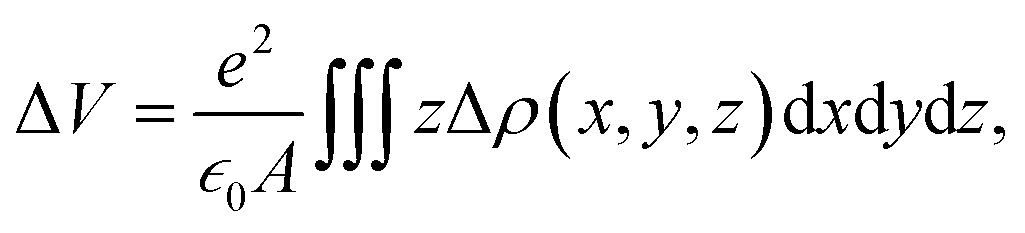
The charge transfer condition at Gr–MoS2 interface is confirmed in electron density redistribution in Fig. 3, which further visualizes the interface coupling between the graphene and MoS2 layers. The electron density difference,Δρ(x, y, z), is an effective tool to analyze the bonding at Gr–MoS2 interfaces which is defined as the difference of the electron density distribution of the composite full system and the isolated subsystems:
| Δρ = ρtot − ρGr − ρMoS2, | (1) |
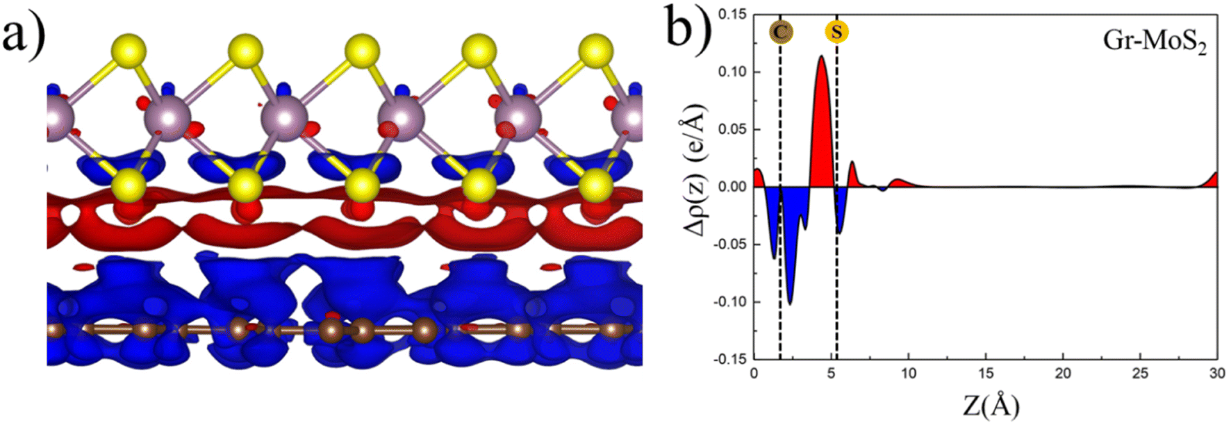 | ||
| Fig. 3 (a) 3D electron density redistribution of Gr–MoS2 heterostructure. The isosurface refers to isovalues of 1 × 10⁻³ e Å−3. (b) The plane-averaged electron density difference Δρ(z) along the z-direction perpendicular to the Gr–MoS2 interfaces. Red (blue) region represents electron accumulation (depletion). The region of interface is indicated by two dotted black lines representing the surface-atom-layers of carbon and sulfur. | ||
According to Poisson equation, the interface dipole ΔV and electron density distribution Δρ satisfies the following relation:
 | (2) |
| ΔV = WGr–MoS2 − WGr, | (3) |
 | ||
| Fig. 4 Projected band structures of MoS2 in Gr–MoS2 heterojunction with strain from −4% (a) to 6% (f). The red point represents the projected band of MoS2, and the size of the point represents the weight. The blue double arrows represent the Schottky barrier height. | ||
Effects of in-plane strain
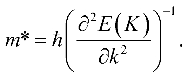
Sequentially, sensitive responses of electronic performances in Gr–MoS2 heterostructure in case of in-plane biaxial compression and tension strains are evaluated. Especially the Schottky barriers at Gr–MoS2 interfaces as indicated by the project band structures of MoS2 in heterojunctions are shown in Fig. 4. By assembly with graphene substrate, the direct band gap of monolayer MoS2 transforms to indirect and an n-type Schottky barrier forms at Gr–MoS2 interface with absence of strain in Fig. 4c. It is observed that with compress strain changes from 2% to 4% in Fig. 4a and b, the VBM and CBM of MoS2 keep at the high symmetry point K, manifesting as a direct band gap. Simultaneously, the EF moves downward to the VBM of MoS2, creating n-type Schottky barriers. However, with tensile strain, the VBM in MoS2 shifts from K to Γ, the CBM keeps at the high symmetry point K, resulting an indirect band gap. When tensile strain varies from 2% to 6%, the Fermi level gradually moves towards the CBM of MoS2, representing a reduction in the n-type Schottky barrier of heterostructure, as illustrated in Fig. 4(d–f). Relatively speaking, although the energy difference from VBM to the Fermi level also decreases with tensile strain, it is always significantly greater than that of CBM to the Fermi level, thus the system vigorously preserves the contact of n-type. It is worth noting that the n-type Schottky barrier turns to ohmic contact at a tensile strain of 6%. It could be speculated that the certain biaxial strain is not only conducive to the occurrence of conversion for the contact types, but also the modulation of the Schottky barrier heights.The band structures of Gr–MoS2 heterojunction are shown in Fig. 5. Since the effective masses are closely associated with carrier motion capacity, therefore the effective mass of graphene in this heterostructure is firstly considered to check whether the superior carrier motion capacity of graphene is maintained. The electron mobility is inversely proportional to the effective mass, which is described as: μ = eτ/m*, where μ is electron mobility, e is the electron charge, m* is the effective electron mass, and τ is the relaxation time. For semiconductors, both electrons and holes contribute to carrier mobility, therefore, the effective masses of holes  and electrons
  of the heterostructure are calculated. The effective masse of electrons and holes are determined by matching parabolic functions to the band structure of CBM and VBM for the wave vectors:48,56
 | (4) |
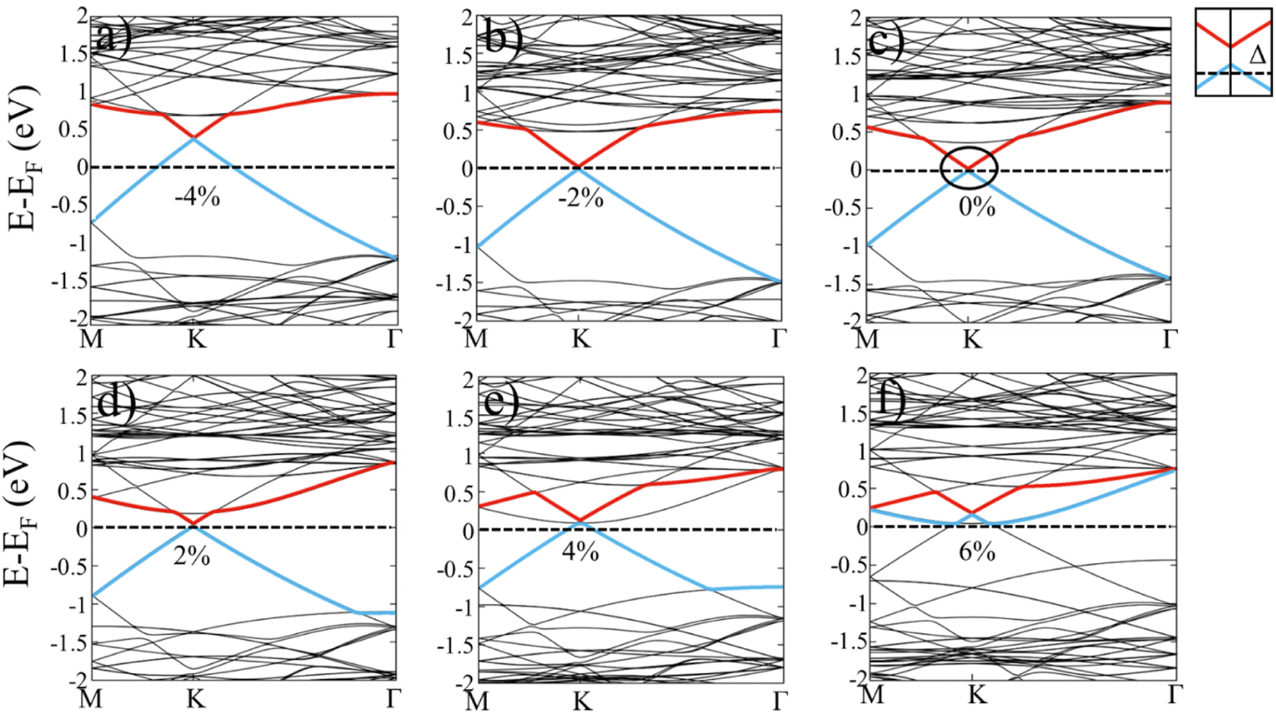 | ||
| Fig. 5 Band structures of the Gr–MoS2 heterostructure under different strain. The blue, and red lines stand respectively for bonding π-band and antibonding π*-band of graphene. (a)–(f) represent the strain of −4%, −2%, 0%, 2%, 4%, and 6%, respectively. Detailed information of Dirac Point is shown. The Fermi level is set to zero and marked by black dotted lines. | ||
As shown in Fig. 5c, the energy band of graphene remains linear near the Dirac point, while the Fermi level in the heterojunction is shifted and lied slightly below the Dirac point of graphene. This is because electrons transfer from graphene to MoS2 which is consistent with the charge transfer results (Fig. 3). In addition, since the small quantity of charge transfer at Gr–MoS2 interface, the Fermi level shift is small, according with the vdW characteristics between graphene and MoS2. When tensile strain is applied, the charge transfer between graphene and MoS2 increase gradually (as shown in Fig. S5†), so that the Fermi level gradually moving away from the Dirac point (Fig. 5d–f).
A tiny band gap of 1.2 meV for graphene in Gr–MoS2 heterostructure is opened at the Dirac point due to sublattice symmetry breaking, shown in Fig. 5c. Based on the π-electron tight-binding (TB) approximation of graphene, the dispersion relation near the Fermi level can be approximated as:
 | (5) |
The C-pz orbitals in isolated graphene and Gr–MoS2 heterojunction are displayed in Fig. 6a, and it is obvious that the CBM and VBM at Dirac point are both contributed by the C-pz orbital electrons in both systems. In comparison with freestanding graphene, the PDOS of the C-pz orbitals in heterostructure are more local. Furthermore, the PDOS of C-pz, S-p, and Mo-d orbitals in Gr–MoS2 heterojunction are shown in Fig. 6b, and a weak hybridization is formed between the C-pz of graphene and S-p orbitals of the MoS2, as marked by a green circle. Therefore, after the deposition of MoS2, the symmetry of graphene is broken, and the interaction of C-pz and S-p in the direction perpendicular to the interface give rise to out-plane sp3 orbitals in graphene, the bonding π and anti-bonding π* bands repulse each other, forming an energy gap at Dirac point.60,61 As tensile strain is applied, the interaction between MoS2 and graphene becomes stronger, a larger band gap has been opened. Additionally, a maximum gap of 2.6 meV is obtained when 6% tensile strain is imposed.
 | ||
| Fig. 6 Partial density of states (PDOS) of (a) C-pz orbitals in isolated graphene and in Gr–MoS2 heterojunction; and (b) C-pz, S-p, and Mo-d orbitals in Gr–MoS2 heterojunction. The Fermi energy level is set to be zero. | ||
Conclusions
In conclusion, the structural optimizations and electronic characteristics of Gr–MoS2 vdW heterostructure are explored under the applied in-plane biaxial strains through first-principles calculations. The heterostructure is formed by the weak interlayer coupling with the typical vdW binding energy of 0.35 J m−2. In Gr–MoS2 heterojunctions, the electronic band structure of graphene and MoS2 are preserved well, with an n-type SBH of 0.33 eV is obtained at the equilibrium state with absence of strain, which may be effectively adjusted via imposing the in-plane biaxial strains. Especially, the n-type Schottky contact transform to ohmic contact when the tensile strain is greater than 6%. In contrast to metal-MoS2 contacts, the Gr–MoS2 interface presents a negligible interface dipole, implying that the SBH at the interface can be obtained from the freestanding layers by aligning the vacuum levels. The linear Dirac-like dispersion relation around the Fermi level of graphene is still preserved in Gr–MoS2 interface. In addition, a tiny band gap of 1.2 meV of Gr–MoS2 interface is opened at the Dirac K-point of graphene, and the bandgap increase to 2.6 meV when 6% tensile strain is applied. The appearance of the energy band gap of graphene has opened up new possibilities for using it in graphene-based device applications. Moreover, in-plane strain can be used as an effective means to regulate the Schottky barrier.Conflicts of interest
There are no conflicts of interest to declare.Acknowledgements
This work was financially supported by Natural Science Foundation of Hubei Province of China (No. 2020CFB245), teaching research projects in Colleges and Universities of Hubei (No. 2020668), National Natural Science Foundation of China (22101198, 51801057), research start-up funding of Hubei University of Education (19RC03, ESRC20220030), teaching research project of Hubei University of Education (X2019007).References
- Y. Zhao, M. Gobbi, L. E. Hueso and P. Samori, Molecular Approach to Engineer Two-Dimensional Devices for CMOS and beyond-CMOS Applications, Chem. Rev., 2022, 122, 50–131 CrossRef CAS PubMed.
- E. C. Ahn, 2D materials for spintronic devices, npj 2D Mater. Appl., 2020, 4, 17 CrossRef CAS.
- G. G. Naumis, S. Barraza-Lopez, M. Oliva-Leyva and H. Terrones, Electronic and optical properties of strained graphene and other strained 2D materials: a review, Rep. Prog. Phys., 2017, 80, 1–62 CrossRef PubMed.
- Y. Dong, C. Yan, H. Zhao and Y. Lei, Recent Advances in 2D Heterostructures as Advanced Electrode Materials for Potassium-Ion Batteries, Small Struct., 2022, 3, 2100221 CrossRef CAS.
- K. S. Novoselov, A. K. Geim, S. V. Morozov, D. Jiang, Y. Zhang, S. V. Dubonos, I. V. Grigorieva and A. A. Firsov, Electric Field Effect in Atomically Thin Carbon Films, Science, 2004, 306, 666–669 CrossRef CAS PubMed.
- A. H. Castro Neto, F. Guinea, N. M. R. Peres, K. S. Novoselov and A. K. Geim, The electronic properties of graphene, Rev. Mod. Phys., 2009, 81, 109–162 CrossRef CAS.
- P. V. Pham, S. C. Bodepudi, K. Shehzad, Y. Liu, Y. Xu, B. Yu and X. Duan, 2D Heterostructures for Ubiquitous Electronics and Optoelectronics: Principles, Opportunities, and Challenges, Chem. Rev., 2022, 122, 6514–6613 CrossRef CAS PubMed.
- K. Shi, J. Su, H. Liang, K. Hu and J. Xu, Highly optically transparent graphene mesh for electromagnetic interference shielding, Diamond Relat. Mater., 2022, 123, 108849 CrossRef CAS.
- K. F. Mak, C. Lee, J. Hone, J. Shan and T. F. Heinz, Atomically Thin MoS2: A New Direct-Gap Semiconductor, Phys. Rev. Lett., 2010, 105, 136805 CrossRef PubMed.
- H. Liu, A. T. Neal and P. D. Ye, Channel Length Scaling of MoS2 MOSFETs, ACS Nano, 2012, 6, 8563–8569 CrossRef CAS PubMed.
- O. Samy, D. Birowosuto and A. El Moutaouakil, Ieee, A short review on Molybdenum disulfide (MoS2) applications and challenges, 6th International Conference on Renewable Energy-Generation and Applications (ICREGA), United Arab Emirates Univ, Al Ain, U Arab Emirates, ( 2021), pp. 220–222 Search PubMed.
- G. He, K. Ghosh, U. Singisetti, H. Ramamoorthy, R. Somphonsane, G. Bohra, M. Matsunaga, A. Higuchi, N. Aoki, S. Najmaei, Y. Gong, X. Zhang, R. Vajtai, P. M. Ajayan and J. P. Bird, Conduction Mechanisms in CVD-Grown Monolayer MoS2 Transistors: From Variable-Range Hopping to Velocity Saturation, Nano Lett., 2015, 15, 5052–5058 CrossRef CAS PubMed.
- V. K. Sangwan and M. C. Hersam, Electronic Transport in Two-Dimensional Materials, Annu. Rev. Phys. Chem., 2018, 69, 299–325 CrossRef CAS PubMed.
- S. Das, H.-Y. Chen, A. V. Penumatcha and J. Appenzeller, High Performance Multilayer MoS2 Transistors with Scandium Contacts, Nano Lett., 2013, 13, 100–105 CrossRef CAS PubMed.
- D. S. Schulman, A. J. Arnold and S. Das, Contact engineering for 2D materials and devices, Chem. Soc. Rev., 2018, 47, 3037–3058 RSC.
- J. Y. Kwak, J. Hwang, B. Calderon, H. Alsalman, N. Munoz, B. Schutter and M. G. Spencer, Electrical Characteristics of Multilayer MoS2 FET's with MoS2/Graphene Heterojunction Contacts, Nano Lett., 2014, 14, 4511–4516 CrossRef CAS PubMed.
- S. Kang, D. Lee, J. Kim, A. Capasso, H. S. Kang, J.-W. Park, C.-H. Lee and G.-H. Lee, 2D semiconducting materials for electronic and optoelectronic applications: potential and challenge, 2DMaterials, 2020, 7, 022003 CAS.
- S. Gbadamasi, M. Mohiuddin, V. Krishnamurthi, R. Verma, M. W. Khan, S. Pathak, K. Kalantar-Zadeh and N. Mahmood, Interface chemistry of two-dimensional heterostructures-fundamentals to applications, Chem. Soc. Rev., 2021, 50, 4684–4729 RSC.
- J. Shim, D.-H. Kang, Y. Kim, H. Kum, W. Kong, S.-H. Bae, I. Almansouri, K. Lee, J.-H. Park and J. Kim, Recent progress in Van der Waals (vdW) heterojunction-based electronic and optoelectronic devices, Carbon, 2018, 133, 78–89 CrossRef CAS.
- B. Huang, Q. Xu and S.-H. Wei, Theoretical study of corundum as an ideal gate dielectric material for graphene transistors, Phys. Rev. B, 2011, 84, 155406 CrossRef.
- X. Xu, C. Liu, Z. Sun, T. Cao, Z. Zhang, E. Wang, Z. Liu and K. Liu, Interfacial engineering in graphene bandgap, Chem. Soc. Rev., 2018, 47, 3059–3099 RSC.
- F. Varchon, R. Feng, J. Hass, X. Li, B. N. Nguyen, C. Naud, P. Mallet, J. Y. Veuillen, C. Berger, E. H. Conrad and L. Magaud, Electronic Structure of Epitaxial Graphene Layers on SiC: Effect of the Substrate, Phys. Rev. Lett., 2007, 99, 126805 CrossRef CAS PubMed.
- R. Nandee, M. A. Chowdhury, A. Shahid, N. Hossain and M. Rana, Band gap formation of 2D materialin graphene: Future prospect and challenges, Results Eng., 2022, 15, 100474 CrossRef CAS.
- N. Jain, F. Yang, R. B. Jacobs-Gedrim, X. Xu, M. P. Anantram and B. Yu, Extenuated interlayer scattering in double-layered graphene/hexagonal boron nitride heterostructure, Carbon, 2018, 126, 17–22 CrossRef CAS.
- F. Ersan, D. Kecik, V. O. Ozcelik, Y. Kadioglu, O. U. Akturk, E. Durgun, E. Akturk and S. Ciraci, Two-dimensional pnictogens: A review of recent progresses and future research directions, Appl. Phys. Rev., 2019, 6, 021308 Search PubMed.
- D. Qiu and E. K. Kim, Electrically Tunable and Negative Schottky Barriers in Multi-layered Graphene/MoS2 Heterostructured Transistors, Sci. Rep., 2015, 5, 13743 CrossRef PubMed.
- L. Yu, Y.-H. Lee, X. Ling, E. J. G. Santos, Y. C. Shin, Y. Lin, M. Dubey, E. Kaxiras, J. Kong, H. Wang and T. Palacios, Graphene/MoS2 Hybrid Technology for Large-Scale Two-Dimensional Electronics, Nano Lett., 2014, 14, 3055–3063 CrossRef CAS PubMed.
- S. Singh, C. Espejo and A. H. Romero, Structural, electronic, vibrational, and elastic properties of graphene/MoS2 bilayer heterostructures, Phys. Rev. B, 2018, 98, 155309 CrossRef CAS.
- Z. Zhuo, F. Yang, J. Han, X. Cao, Y. Tao, L. Zhang, W. Liu, Z. Zhu and Y. Dai, Substitutional doping at S site of MoS2/G heterostructure: The influence on voltage-current and electronic characteristics, Superlattices Microstruct., 2021, 156, 106978 CrossRef CAS.
- J. N. Coleman, M. Lotya, A. O'Neill, S. D. Bergin, P. J. King, U. Khan, K. Young, A. Gaucher, S. De, R. J. Smith, I. V. Shvets, S. K. Arora, G. Stanton, H. Y. Kim, K. Lee, G. T. Kim, G. S. Duesberg, T. Hallam, J. J. Boland, J. J. Wang, J. F. Donegan, J. C. Grunlan, G. Moriarty, A. Shmeliov, R. J. Nicholls, J. M. Perkins, E. M. Grieveson, K. Theuwissen, D. W. McComb, P. D. Nellist and V. Nicolosi, Two-dimensional nanosheets produced by liquid exfoliation of layered materials, Science, 2011, 331, 568–571 CrossRef CAS PubMed.
- C. Chang, W. Chen, Y. Chen, Y. Chen, Y. Chen, F. Ding, C. Fan, H. J. Fan, Z. Fan, C. Gong, Y. Gong, Q. He, X. Hong, S. Hu, W. Hu, W. Huang, Y. Huang, W. Ji, D. Li, L.-J. Li, Q. Li, L. Lin, C. Ling, M. Liu, N. Liu, Z. Liu, K. P. Loh, J. Ma, F. Miao, H. Peng, M. Shao, L. Song, S. Su, S. Sun, C. Tan, Z. Tang, D. Wang, H. Wang, J. Wang, X. Wang, X. Wang, A. T. S. Wee, Z. Wei, Y. Wu, Z.-S. Wu, J. Xiong, Q. Xiong, W. Xu, P. Yin, H. Zeng, Z. Zeng, T. Zhai, H. Zhang, H. Zhang, Q. Zhang, T. Zhang, X. Zhang, L.-D. Zhao, M. Zhao, W. Zhao, Y. Zhao, K.-G. Zhou, X. Zhou, Y. Zhou, H. Zhu, H. Zhang and Z. Liu, Recent Progress on Two-Dimensional Materials, Acta Phys.-Chim. Sin., 2021, 37, 2108017 Search PubMed.
- D. Yuan, Y. Dou, Z. Wu, Y. Tian, K.-H. Ye, Z. Lin, S. X. Dou and S. Zhang, Atomically Thin Materials for Next-Generation Rechargeable Batteries, Chem. Rev., 2022, 122, 957–999 CrossRef CAS PubMed.
- Y. Ma, Y. Dai, M. Guo, C. Niu and B. Huang, Graphene adhesion on MoS2 monolayer: An ab initio study, Nanoscale, 2011, 3, 3883–3887 RSC.
- G. Kresse and J. Hafner, Ab initio molecular dynamics for liquid metals, Phys. Rev. B, 1993, 47, 558–561 CrossRef CAS PubMed.
- P. E. Blöchl, Projector augmented-wave method, Phys. Rev. B, 1994, 50, 17953–17979 CrossRef PubMed.
- G. Kresse and J. Furthmüller, Efficient iterative schemes for ab initio total-energy calculations using a plane-wave basis set, Phys. Rev. B, 1996, 54, 11169–11186 CrossRef CAS PubMed.
- G. Kresse and D. Joubert, From ultrasoft pseudopotentials to the projector augmented-wave method, Phys. Rev. B, 1999, 59, 1758–1775 CrossRef CAS.
- J. Sun, A. Ruzsinszky and J. P. Perdew, Strongly Constrained and Appropriately Normed Semilocal Density Functional, Phys. Rev. Lett., 2015, 115, 036402 CrossRef PubMed.
- H. Peng, Z.-H. Yang, J. P. Perdew and J. Sun, Versatile van der Waals Density Functional Based on a Meta-Generalized Gradient Approximation, Phys. Rev. X, 2016, 6, 041005 Search PubMed.
- H. Peng and J. P. Perdew, Rehabilitation of the Perdew-Burke-Ernzerhof generalized gradient approximation for layered materials, Phys. Rev. B, 2017, 95, 081105 CrossRef.
- Q. Wang, K. Dou and X. Shi, Band alignment in multilayered semiconductor homojunctions supported on metals, J. Mater. Chem. C, 2020, 8, 959–967 RSC.
- J. Neugebauer and M. Scheffler, Adsorbate-substrate and adsorbate-adsorbate interactions of Na and K adlayers on Al(111), Phys. Rev. B, 1992, 46, 16067–16080 CrossRef CAS PubMed.
- T. Böker, R. Severin, A. Müller, C. Janowitz, R. Manzke, D. Voß, P. Krüger, A. Mazur and J. Pollmann, Band structure of MoS2, MoSe2, and α-MoTe2: Angle-resolved photoelectron spectroscopy and ab initio calculations, Phys. Rev. B, 2001, 64, 235305 CrossRef.
- A. A. Al-Hilli and B. L. Evans, The preparation and properties of transition metal dichalcogenide single crystals, J. Cryst. Growth, 1972, 15, 93–101 CrossRef CAS.
- J. Shi, L. Chen, M. Yang, Z. Mi, M. Zhang, K. Gao, D. Zhang, S. Su and W. Hou, Interface contact and modulated electronic properties by external vertical strains and electric fields in graphene/MoS2 heterostructure, Curr. Appl. Phys., 2022, 39, 331–338 CrossRef.
- K. Y. Thai, I. Park, B. J. Kim, A. T. Hoang, Y. Na, C. U. Park, Y. Chae and J.-H. Ahn, MoS2/Graphene Photodetector Array with Strain-Modulated Photoresponse up to the Near-Infrared Regime, ACS Nano, 2021, 15, 12836–12846 CrossRef CAS PubMed.
- Q. Wang, B. Deng and X. Shi, A new insight for ohmic contacts to MoS2: by tuning MoS2 affinity energies but not metal work-functions, Phys. Chem. Chem. Phys., 2017, 19, 26151–26157 RSC.
- X. Lu, L. Li, X. Guo, J. Ren, H. Xue and F. Tang, The controllable electronic characteristics and Schottky barrier of graphene/GaP heterostructure via interlayer coupling and in-plane strain, Mater. Sci. Eng., B, 2022, 284, 115882 CrossRef CAS.
- W. Xiong, C. Xia, X. Zhao, T. Wang and Y. Jia, Effects of strain and electric field on electronic structures and Schottky barrier in graphene and SnS hybrid heterostructures, Carbon, 2016, 109, 737–746 CrossRef CAS.
- M. Sun, J.-P. Chou, J. Yu and W. Tang, Effects of structural imperfection on the electronic properties of graphene/WSe2 heterostructures, J. Mater. Chem. C, 2017, 5, 10383–10390 RSC.
- A. C. Ferrari, J. C. Meyer, V. Scardaci, C. Casiraghi, M. Lazzeri, F. Mauri, S. Piscanec, D. Jiang, K. S. Novoselov, S. Roth and A. K. Geim, Raman Spectrum of Graphene and Graphene Layers, Phys. Rev. Lett., 2006, 97, 187401 CrossRef CAS PubMed.
- E. Wang, X. Lu, S. Ding, W. Yao, M. Yan, G. Wan, K. Deng, S. Wang, G. Chen, L. Ma, J. Jung, A. V. Fedorov, Y. Zhang, G. Zhang and S. Zhou, Gaps induced by inversion symmetry breaking and second-generation Dirac cones in graphene/hexagonal boron nitride, Nat. Phys., 2016, 12, 1111–1115 Search PubMed.
- H. Li, Z. Zhou and H. Wang, Tunable Schottky barrier in InTe/graphene van der Waals heterostructure, Nanotechnology, 2020, 31, 335201 CrossRef CAS PubMed.
- W. Hu, T. Wang, R. Zhang and J. Yang, Effects of interlayer coupling and electric fields on the electronic structures of graphene and MoS2 heterobilayers, J. Mater. Chem. C, 2016, 4, 1776–1781 RSC.
- M. Farmanbar and G. Brocks, First-principles study of van der Waals interactions and lattice mismatch at MoS2/metal interfaces, Phys. Rev. B, 2016, 93, 085304 CrossRef.
- B. Zhou, X. Wang, S. Dong, K. Zhang and W. Mi, Tunable gap opening and spin polarization of two dimensional graphene/hafnene van der Waals heterostructures, Carbon, 2017, 120, 121–127 CrossRef CAS.
- I. N. Yakovkin, Dirac Cones in Graphene, Interlayer Interaction in Layered Materials, and the Band Gap in MoS2, Crystals, 2016, 6, 143 CrossRef.
- H. V. Phuc, N. N. Hieu, B. D. Hoi, L. T. T. Phuong and C. V. Nguyen, First principle study on the electronic properties and Schottky contact of graphene adsorbed on MoS2 monolayer under applied out-plane strain, Surf. Sci., 2018, 668, 23–28 CrossRef CAS.
- H. V. Phuc, N. N. Hieu, B. D. Hoi and C. V. Nguyen, Interlayer coupling and electric field tunable electronic properties and Schottky barrier in a graphene/bilayer-GaSe van der Waals heterostructure, Phys. Chem. Chem. Phys., 2018, 20, 17899–17908 RSC.
- H. Coy Diaz, J. Avila, C. Chen, R. Addou, M. C. Asensio and M. Batzill, Direct Observation of Interlayer Hybridization and Dirac Relativistic Carriers in Graphene/MoS2 van der Waals Heterostructures, Nano Lett., 2015, 15, 1135–1140 CrossRef CAS PubMed.
- D. Pierucci, H. Henck, J. Avila, A. Balan, C. H. Naylor, G. Patriarche, Y. J. Dappe, M. G. Silly, F. Sirotti, A. T. C. Johnson, M. C. Asensio and A. Ouerghi, Band Alignment and Minigaps in Monolayer MoS2-Graphene van der Waals Heterostructures, Nano Lett., 2016, 16, 4054–4061 CrossRef CAS PubMed.
Footnote |
| † Electronic supplementary information (ESI) available. See DOI: https://doi.org/10.1039/d2ra07949f |
| This journal is © The Royal Society of Chemistry 2023 |