
 Open Access Article
 This Open Access Article is licensed under a Creative Commons Attribution-Non Commercial 3.0 Unported Licence
Femtosecond laser patterned silicon embedded with gold nanostars as a hybrid SERS substrate for pesticide detection†
Sree Satya Bharati Moram a,
Chandu Byramb and
Venugopal Rao Soma*a
a,
Chandu Byramb and
Venugopal Rao Soma*a
aAdvanced Centre for Research in High Energy Materials (ACRHEM), DRDO Industry Academia–Centre of Excellence (DIA-COE), University of Hyderabad, Prof. C. R. Rao Road, Hyderabad 500046, Telangana, India. E-mail: soma_venu@uohyd.ac.in; soma_venu@yahoo.com
bDepartment of Physics, College of Arts and Sciences, University of Dayton, 300 College Park, Dayton, Ohio 45469, USA
First published on 17th January 2023
Abstract
We have developed simple and cost-effective surface-enhanced Raman scattering (SERS) substrates for the trace detection of pesticide (thiram and thiabendazole) and dye (methylene blue and Nile blue) molecules. Surface patterns (micro/nanostructures) on silicon (Si) substrates were fabricated using the technique of femtosecond (fs) laser ablation in ambient air. Different surface patterns were achieved by tuning the number of laser pulses per unit area (4200, 8400, 42![[thin space (1/6-em)]](https://www.rsc.org/images/entities/char_2009.gif) 000, and 84000 pulses per mm2) on Si. Subsequently, chemically synthesized gold (Au) nanostars were embedded in these laser-patterned areas of Si to achieve a plasmonic active hybrid SERS substrate. Further, the SERS performance of the as-prepared Au nanostar embedded Si substrates were tested with different probe molecules. The as-prepared substrates allowed us to detect a minimum concentration of 0.1 ppm in the case of thiram, 1 ppm in the case of thiabendazole (TBZ), 1.6 ppb in the case of methylene blue (MB), and 1.8 ppb in case of Nile blue (NB). All these were achieved using a simple, field-deployable, portable Raman spectrometer. Additionally, the optimized SERS substrate demonstrated ∼21 times higher SERS enhancement than the Au nanostar embedded plain Si substrate. Furthermore, the optimized SERS platform was utilized to detect a mixture of dyes (MB + NB) and pesticides (thiram + TBZ). The possible reasons for the observed additional enhancement are elucidated.
000, and 84000 pulses per mm2) on Si. Subsequently, chemically synthesized gold (Au) nanostars were embedded in these laser-patterned areas of Si to achieve a plasmonic active hybrid SERS substrate. Further, the SERS performance of the as-prepared Au nanostar embedded Si substrates were tested with different probe molecules. The as-prepared substrates allowed us to detect a minimum concentration of 0.1 ppm in the case of thiram, 1 ppm in the case of thiabendazole (TBZ), 1.6 ppb in the case of methylene blue (MB), and 1.8 ppb in case of Nile blue (NB). All these were achieved using a simple, field-deployable, portable Raman spectrometer. Additionally, the optimized SERS substrate demonstrated ∼21 times higher SERS enhancement than the Au nanostar embedded plain Si substrate. Furthermore, the optimized SERS platform was utilized to detect a mixture of dyes (MB + NB) and pesticides (thiram + TBZ). The possible reasons for the observed additional enhancement are elucidated.
Introduction
Surface-enhanced Raman scattering (SERS) is a widely recognized and approved spectroscopic tool because of its high sensitivity. This technique has been extensively used in innumerable applications over the last decade.1,2 In general, the analyte molecule's Raman signal amplification relies upon localized electric fields on a metallic substrate (EM) and electron transfer between the analyte and metal (CT). Pesticides are typically used in agriculture to protect crops and their products. However, most used pesticides enter the environment (soil) and agricultural products, including fruits and vegetables. Even trace amounts of pesticides gradually cause health risks to all creatures and pollute the agricultural environment. The advantage of the fingerprint-based SERS technique is quick and can be applied to detect pesticide residues in a real-life scenario. Over the past few decades, different sizes/shapes of noble metal colloids have been extensively used as SERS substrates.3 Among all the various types of nanostructures, gold nanostars and multi-branched gold nanoparticles are promising candidates due to their plasmon band quality.4 Notably, substantial electric field enhancements are present at the sharp tips and edges of Au nanostars because of the they support high surface charge density required for activating localized surface plasmon polariton. The confined field enhancement at sharp tips/edges acts as excellent “hot spots” for the Raman signal enhancement.5–10 Chang et al.11 reported the detection of the Raman signal of the analyte (4-mercaptobenzoic acid) with a single Au nanostar and without the need for NPs aggregation/assembly or resonant excitation wavelength of the analyte used. Chung et al.12 numerically studied the effect of the core size, spikes number, and spike tip angle on the SERS enhancement factors. Guerrero et al.13 reviewed the various fabrication procedures for the colloidal gold nanostars synthesis and demonstrated the promising applications in SERS and catalysis etc. Recently, a heterogeneous SERS substrate attracted significant attention to achieve further enhancement from the colloidal nanostars. Instead of depositing those colloids on a plain substrate such as silicon/glass, it is believed that rough surfaces will further strengthen the Raman signal of the analyte molecule because of its high surface-to-volume ratio, which allows it to generate more hotspots and capture more molecules within the probing area. Wu et al.14 fabricated Au nanoparticles embedded in nano-porous silicon SERS substrate through the immersion plating technique and subsequently detected methylene blue molecule at minute concentrations (μM). Chang et al.11 fabricated Ag NPs on Si substrate by simple replacement reduction method and demonstrated the detection of R6G and melamine in different aqueous media. Kang et al.15 have synthesized 24-faced PbS–Au hybrids SERS substrates through a steerable hydrothermal strategy. These SERS substrates efficacy was tested with a model Raman molecule of Rhodamine B and achieved the analytical enhancement factor up to ∼108 with a minimal detection limit of 10−12 M.16 Yan et al.17 investigated the Cu(110) triangular micro-cavity arrays that were synthesized using a tip-based force-modulated indention method. Subsequently, they have performed the detection studies on R6G and obtained enhancement factors (EFs) of ∼106. SERS substrates having rough surfaces with micro/nano features have found a great deal of attention in a wide range of fields and can be fabricated using numerous methods including electrochemical, lithography, electrochemical etching, laser ablation, etc.18–21 Among those diverse approaches, ultrafast laser ablation is a versatile technique that can induce various surface patterns on solid substrates like two/three-dimensional micro/nanostructures on diverse materials (metals, semiconductors, dielectrics, polymers, etc.).22,23 Previously, our group has reported the fabrication of various laser-induced surface structures as well as nanoparticles (NPs) utilizing various materials. Further, the as-prepared NPs and nanostructures were efficiently used for the SERS-based detection of diverse analytes, including explosives and dyes.24–26 Even though the patterned Si materials are not strongly active SERS substrates, they do demonstrate an enhancement in the Raman signals due to the photo-induced charge transfer mechanism.27 Few reports have demonstrated the EFs of ∼106 using Si web-like structures, ∼103 using Si nanowires and nanocones, and ∼510 using Si Nano-pillars, etc.28–30 Herein, we have developed a hybrid-based SERS substrates composed of laser-patterned Si substrates and Au nanostars achieved using a simple approaches of femtosecond laser ablation and chemical method, respectively. Different patterns on Si substrates were achieved by varying the number of pulses and then coated with chemically prepared Au nanostars. Further, the Au nanostars embedded fs laser-patterned Si surfaces were efficaciously utilized for the detection of pesticides, dyes and their mixtures using the SERS approach. The Raman enhancements are attributed to the strong electric field at the sharp tips and plasmonic coupling between the Au nanostars decorated on roughened SiO2.Experimental details
Fabrication of micro/nano patterns on silicon using laser irradiation
Si micro/nanostructures were fabricated using a Ti: sapphire femtosecond (fs) laser system (LIBRA, M/s Coherent) delivering ∼50 fs pulses at a central wavelength of 800 nm and a repetition rate of 1 kHz. The Si wafer (99.9%, Sigma-Aldrich) with dimension 1 × 1 cm2 was placed on the holder and then mounted on the motorized X–Y stage (Newport, USA), controlled by a computer. The focused fs laser beam was guided onto the Si surface using a plano-convex lens (focal length ∼100 mm). Multiple linear and squared array patterns were created over the area of 5 × 5 mm2 on Si by controlling the stage parameters (velocities x = y = 5 mm s−1 and x = y = 0.5 mm s−1 with a line pitch of 50 μm). Further, the estimated number of laser pulses per mm2 on the Si is (1) 4200 for Si at 5 mm s−1 line-pattern (denoted as Si_5L), (2) 8400 for Si at 5 mm s−1 cross-pattern (denoted Si_5C), (3) 42000 for Si at 0.5 mm s−1 line-pattern (denoted as Si_0.5L), and (4) 84000 for Si at 0.5 mm s−1 cross-pattern (denoted as Si_0.5C). The laser-induced NSs were denoted as Si_5L, Si_5C, Si_0.5L, and Si_0.5C for their respective pulse numbers. All the laser patterns on the Si substrate were achieved with a constant pulse energy of ∼30 μJ. A simple procedure was utilized for Au nanostars fabrication.31 Briefly, PVP (2.5 mM) was dissolved in DMF mixed with NaOH (1.5 mM) and HAuCl4·3H2O (0.27 mM), and the solution was stirred using a magnetic stirrer, the color of the solution was changed to blue after 30 minutes. Further, any excess amount of polymer was removed from the colloidal solution by centrifuging it four times in ethanol solvent. Subsequently, Au nanostars were dispersed in 5 mL of ethanol for 10 minutes using an ultrasonicator.
The surface morphology of laser-created patterns on the Si substrate was inspected by a field emission scanning electron microscope (FESEM, Carl Zeiss) operated at 30 kV, and elemental compositions were recorded with the same instrument equipped with an Energy dispersive X-ray spectroscopy (EDX). The 3D topography images of laser-patterned Si surfaces were obtained by atomic force microscope (AFM Oxford Instrument, MFP3D). The optical absorption measurements for Au colloids were conducted using a UV-visible absorption spectrometer (JASCO V-670). Further, the Au nanostars' crystallinity was investigated by recording the X-ray diffraction (XRD) pattern, and their shape and sizes were confirmed by conducting the TEM (FEI TecnaiG2 S-Twin) measurements. For TEM characterization studies, a tiny drop of 2 μL colloidal solution was deposited on a carbon-coated copper grid and then dried at room temperature. Various analyte molecules such as methylene blue (MB-C16H18ClN3S) – 0.1 M, Nile blue (NB-C20H20ClN3O) – 0.1 M, thiram −5 mM, and thiabendazole (TBZ) – 50 mM were initially prepared in-stock solution, and then diluted successively to attain desired lower concentrations. Finally, the SERS substrates were accomplished by dropping 10 μL of Au nanostars suspensions on the laser-patterned Si areas. Later, the SERS investigations were done for the earlier mentioned analytes (quantity of 10 μL) by depositing them onto the Au nanostars decorated laser-patterned Si substrates. The Raman data were acquired with a portable Raman spectrometer (i-Raman plus, M/s B&W Tek, USA) equipped with a continuous laser emitting a wavelength of 785 nm and the spot size of the laser on the sample ∼100 μm. During the Raman measurements, the laser power was set to ∼30 mW and an integration time of 5 s. All the recorded spectra were baseline-corrected using Origin software.
Results and discussion
Characterization studies
Fig. 1(a)–(d) illustrate the FESEM micrographs recorded at lower and higher magnifications. The surface topography images were collected using AFM, which are shown in Fig. 1(e) and (f) (denoted as Si_5L and Si_5C). The micro-spikes around the nanoprotrusions/nano-holes occurred along the laser scan path. From Fig. 1(a) and (b), it is evident that the width of the crater was ∼30 μm and the non-interacted area width was about ∼20 μm with a line spacing of ∼50 μm. The laser-patterned regions consisted of micro-spikes and re-deposited Si nanoparticles, which are evident in Fig. 1(a)–(d). The observed surface features on the Si could be attributed to the melting of the target surface with an intense laser pulse interaction which might have led to the surface tension gradient of molten silicon, which subsequently was possibly dragged from hotter zones to colder zones. Thus, the melted material solidified on the surface leading to the creation of nano spikes/nano craters along the laser scan path. In the case of crossed pattern, many pulses interacted with the target surface leading to the formation of a higher number of micro-spikes with nanoclusters as compared to the linear pattern, which is apparent from the FESEM micrographs presented in Fig. 1(a)–(d). Liang et al.32 demonstrated the observation of grid arrays, droplet arrays, and ultrafine periodic surface structures along the fs laser scan path on the Si substrate, and those nano surface structures are attributed to the Coulomb explosion, ultrafast melting, interference, and local field arrangement. Fig. 1(e) and (f) depict the AFM images of linear and crossed-patterned (obtained at higher scan speed) Si surfaces, respectively. The surface roughness of Si_5L and Si_5C were estimated from “Ra” (the arithmetic average of the absolute value of the surface height deviations measured from the mean plane) and “Rq” (the root-mean-square average of height deviation taken from the mean image data plane). The roughness values of Si_5L were Ra = ∼593.780 nm, Rq = ∼593.785 nm and for that of Si_5C, were Ra = ∼620.228 nm, Rq = ∼620.233 nm. As expected, in the case of crossed patterns, a large number of ablated particles were re-deposited onto the Si surface compared to the linear patterned Si surface under laser irradiation leading to the increase of roughness of the laser-scanned areas of Si. Fig. 2 shows the lower and higher magnification images of linear and crossed-patterned Si samples at low-speed laser scanning (0.5 mm s−1). The lower scan speed resulted in a greater number of pulses interaction at the target surface, yielding a large crater depth (∼μm) compared to the higher scanning speed. The nano periodic surface structures, along with the spherical nanoclusters, were observed near the microgrooves in the case of Si_0.5L [shown in Fig. 2(a) and (b)]. Compared to the linear Si_0.5L, the crossed Si_0.5C substrate comprised deeper grooves surrounded with a large number of ablated species which is evident from the illustrated images in Fig. 2(c) and (d).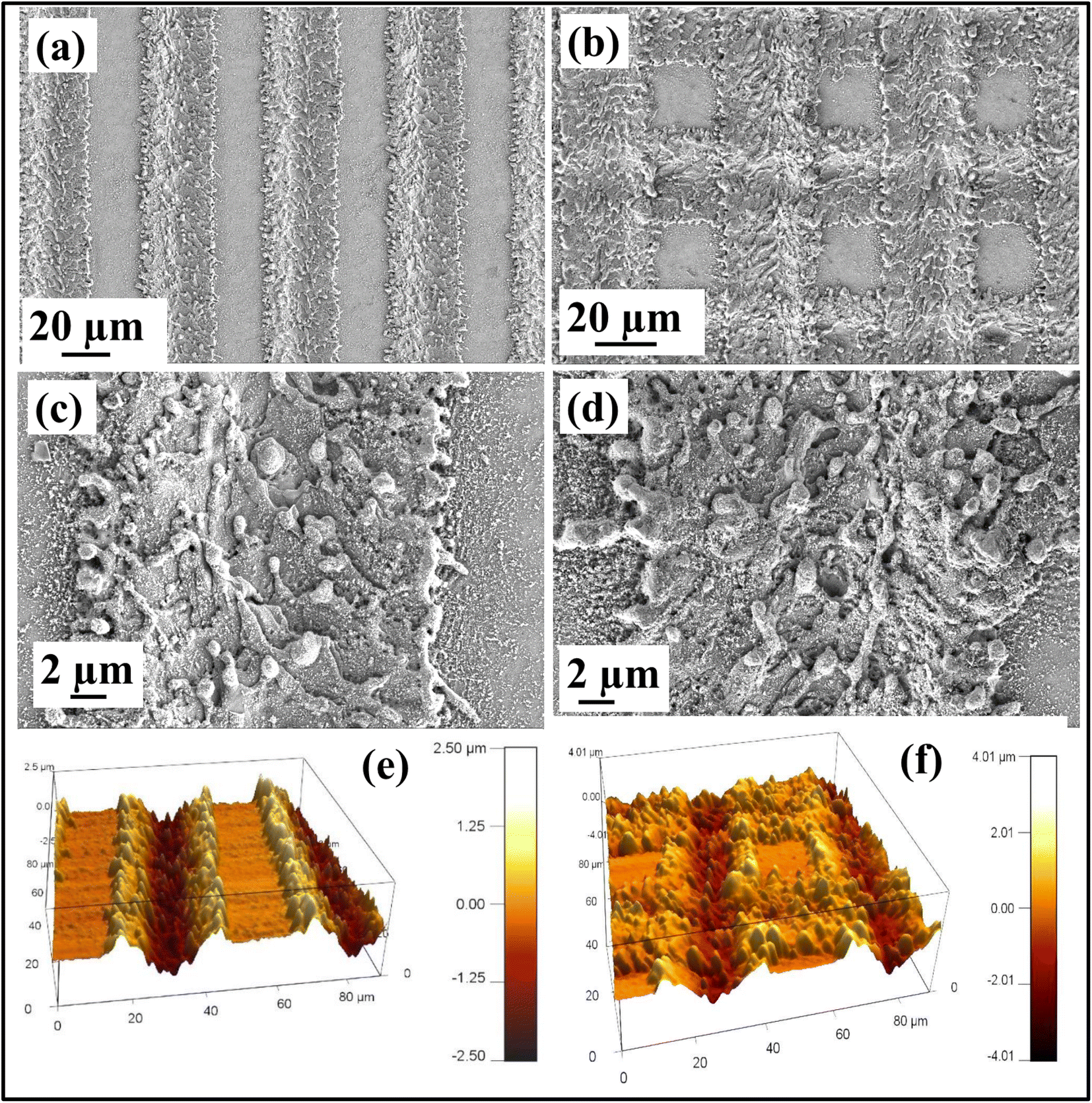 | ||
| Fig. 1 (a, b) and (c, d) Lower and higher magnification FESEM images (e and f) AFM images of Si_5L and Si_5C, respectively. | ||
 | ||
| Fig. 2 Lower and higher magnification FESEM images of Si_0.5L at (a) lower magnification and (b) higher magnification. Images of Si_0.5C at (c) lower magnification and (d) higher magnification. | ||
The energy-dispersive X-ray analysis was performed using FESEM-EDX to confirm the chemical composition of laser-patterned Si substrates. The EDX measurements were conducted on linear and crossed patterned Si surfaces fabricated at various pulse numbers Si_5L (4200 pulses per mm2), Si_5C (8400 pulses per mm2), Si_0.5L (42000 pulses per mm2), and Si_0.5C (84000 pulses per mm2) were shown in Fig. 3(a)–(d). The insets depict the corresponding elemental composition of silicon and oxygen, which reveals the extent of the formation of silicon oxide. The degree of oxidation on the laser-patterned Si surface was observed to increase (O wt% was observed to increase from ∼5 to ∼26) since the number of pulses increased from 4200 to 84000, which could probably be attributed to the increased atomization of oxygen from the surrounding air. The laser plasma plume is produced on the sample surface and discharged at high speed. Typically, it collides with oxygen molecules in the air and ionizes them, causing oxygen ions to enter the silica group and thus increase oxidation.33,34 At the lower scanning speed of 0.5C, more ablative particle deposition led to a more obvious oxidation on the Si surface.35,36
 | ||
| Fig. 3 EDX spectra of laser ablated silicon (a) Si_5L (b) Si_5C (c) Si_0.5L (d) Si_0.5C (inset elemental distribution wt%). | ||
Fig. 4(a) and (b) show the TEM and HRTEM micrographs of as-prepared Au nanostars. TEM images revealed the well-dispersed nanostars (typically 50 nm core with four to eight tips). The d-spacing value was estimated from the HRTEM image to be ∼0.24 nm, which is attributed to the (111) zone axis presented in Fig. 4(b). The inset shows the inverse fast Fourier transform (IFFT) image of the selected region (yellow color). Fig. 4(c) represents the UV-visible absorption spectra of Au colloids, which exhibited two broad (but distinct) LSPR bands, a weaker band or shoulder located at a visible range of 500–600 nm and an intense band typically at NIR range of 650–1000 nm with the peak centered at ∼945 nm. The first weaker band is attributed to the collective electron oscillations of the core, and the second strong band is attributed to the electron oscillations along the sharp edges, i.e., tip-to-tip. Fig. 4(d) represents the XRD spectrum of the Au nanostars. The peak maxima are located at 38.3°, 44.5°, 64.9°, and 77.8°, and these correspond to the Bragg reflections of Au from the planes (1 1 1), (2 0 0), (2 2 0), (3 1 1), and (2 2 2), respectively. The diffraction peaks matched exactly with the previous reports.31
 | ||
| Fig. 4 (a and b) TEM and HRTEM images, inset of (b) show the IFFT of the highlighted area (yellow square), (c) UV-visible absorption spectra, and (d) XRD pattern of Au nanostars. | ||
Fig. 5 depicts the FESEM images of Au nanostars deposited on the plain Si and laser-patterned Si surfaces. The distribution of the Au nanostars is illustrated in 5(a) for plain Si. In Fig. 5(b), the distribution is that of the nanostars on the silicon surface where the debris is deposited (laser pulses did not interact with the surface in this case). In Fig. 5(c) and (d), the distribution is illustrated for the case of laser-patterned Si micro/nanostructures (different areas of same magnification). The Au nanostars were distributed randomly on the plain surface and in the laser-ablated regions of Si. Generally, nanostars exhibit multiple field enhancements due to interactions at the core-sharp tip, tip-to-tip. Further, the enhancements depend on the applied field direction, the number of tips, and the sharpness of the tip edges. The large surface area of laser-patterned Si surfaces facilitates the immobilization of more nanostars. This might have led to the generation of multiple hot spots during SERS measurements. It is to be noted here that the spot size in our Raman measurements was 90–100 μm resulting in covering a large number of nanostars.
 | ||
| Fig. 5 Lower and higher magnification FESEM images of NPs deposited (a) plain Si, (b) untreated Si-redeposited Si NPs, (c) within the groove, (d) on the micro-spikes edge of the ablated line. | ||
SERS studies
To characterize the SERS performance of Au nanostars embedded laser-patterned Si SERS substrates, MB and NB were utilized as model molecules. Fig. 6(a) and (b) present the acquired SERS spectra of MB (at a concentration of 1.6 ppb) and NB (at a concentration of 1.8 ppb) from Au nanostars embedded (i) plain Si, (ii) Si_5L, (iii) Si_5C, (iv) Si_0.5L, and (v) Si_0.5C, respectively. All the important Raman modes were identified and marked in Fig. 6. The characteristic peaks of MB and NB observed in this study matched with earlier works reported recently.37 All the SERS substrates have exhibited a strong and sharp Raman scattering peak at 1620 cm−1 for MB, associated with the ring stretching of C–C and 590 cm−1 peaks for NB, corresponding to the C–C–C and C–N–C deformations, respectively. The complete peaks and their assignments are provided in ESI (Table T1).† | ||
| Fig. 6 SERS spectra (a) MB (1.6 ppb) (b) NB (1.8 ppb) using Au nanostars embedded on (i) plain Si, (ii) Si_5L (iii) Si_5C(iv) Si_0.5L (v) Si_0.5C. The molecular structure is also depicted in the figures. | ||
Unlike planar Si substrates used in previous studies, laser-patterned surfaces exhibited an enormous enhancement due to the accommodation of a huge number of Au nanostars in the micro/nano dimensional areas. The larger surface area of micro spikes/nanoclusters possibly provided an outstanding density of the closely packed Au nanostars with a large cross-section leading to the generation of a large number of hotspots, where the fields are further amplified in narrow gaps between interacting particles. Chang et al.38 demonstrated that the pyramidal Si structures have improved the light capturing and multiple light reflections. Additionally, they have also proposed that the more surface area of the pyramid structures decorated with Ag NPs could have contributed additional Raman signal enhancement for R6G than the flat Si with Ag NPs. Tan et al.39 noticed a substantial improvement in the Raman signal of the R6G molecule from the fs laser-treated Si surface coated with NPs than the flat Si surface with NPs. The estimated enhancement factors (EFs) of MB (for 1620 cm−1 peak) were found to be 4.05 × 10⁷, 8.17 × 10⁷, 1.55 × 10⁸, 2.97 × 10⁸ and 3.79 × 10⁸ while in the case of NB (for 590 cm−1 peak) they were estimated to be 6.82 × 10⁸, 1.87 × 10⁹, 2.4 × 10⁹, 3.27 × 10⁹, and 5.53 × 10⁹ for plain Si, Si_5L, Si_5C, Si_0.5L and Si_0.5C with Au nanostars respectively. Compared with Au nanostars embedded in plain Si, the Raman intensities for the important peaks of MB and NB have significantly amplified from Au nanostars embedded in laser-patterned Si SERS substrates. The as-fabricated Au nanostars embedded Si_5L, Si_5C, Si_0.5L, and Si_0.5C substrates have exhibited 2-, 3-, 7-, and 9-times improvement in the SERS EFs for MB molecule and 3-, 4-, 5-, and 8-times improvement in the EFs of NB molecule than the Au nanostars embedded plain Si substrate. Fig. 7 depicts the obtained EFs for different substrates in which it is evident that the Au nanostars embedded Si_0.5C has shown the best SERS performance among the others.
 | ||
| Fig. 7 The obtained EFs of MB and NB with Au nanostars embedded in plain Si and laser-pattered Si substrates. | ||
Further, we have also tested Au nanostars embedded laser-patterned substrates with thiram (pesticide) at 0.1 ppm concentration. Fig. 8(a) presents the enhanced Raman spectra of thiram-0.1 ppm recorded from Au nanostars embedded (i) plain Si, (ii) Si_5L, (iii) Si_5C, (iv) Si_0.5L, and (v) Si_0.5C substrates. From all the SERS substrates, thiram's four most obvious peaks were located at 566 cm−1, 1139 cm−1, 1370 cm−1, and 1492 cm−1 (depicted in Fig. 8). The intense Raman peak of thiram at 1370 cm−1 can be associated with the CH3 symmetric in-plane deformation and C–N stretching.40 The Raman spectra of thiram is shown in Fig. S1 (ESI†) and observed vibrational peaks with their corresponding mode assignments are tabulated in Table T2 (ESI†). The calculated EFs for the strongest Raman band of thiram positioned at 1370 cm−1 were found to be 6.03 × 10³, 1.93 × 10⁴, 8.31 × 10⁴, 2.39 × 10⁴ and 1.30 × 10⁵ for Au nanostars embedded plain Si, Si_5L, Si_5C, Si_0.5L, and Si_0.5C substrates, respectively. From the obtained results, we could conclude that ∼21.5 times higher SERS enhancement was attained from Au nanostars-embedded laser-patterned Si (denoted as Si_0.5C) substrate than the Au nanostars embedded plain Si SERS substrate. Further, the Raman measurements are performed with Si_0.5C substrate without Au nanostars using TBZ 25 mM molecule. And noticed an increase of the Raman signal at 1578 cm−1 ∼3.5 times compared to bare silicon without Au nanostars, spectra was provided in the ESI S3.† The observed superior SERS enhancement from the Si_0.5C substrate could have originated from their morphological differences as well as the accumulation of nanostars, which possibly led to the generation of numerous hot spots in the grooved surface areas of the Si_0.5C substrate. Additionally, there could be a small contribution from the chemical enhancement of the SiO2 nanostructures (the presence of oxygen in these nanostructures was confirmed from the EDX data). Previously, laser-ablated Si/Ag micro/nanostructures decorated with spherical NPs were studied, and the NSs decorated with spherical NPs demonstrated a superior sensitivity as compared to the plain substrate.26,41
 | ||
| Fig. 8 (a) SERS spectra of thiram 0.1 ppm using (i) plain Si, (ii) Si_5L, (iii) Si_5C, (iv) Si_0.5L (v) Si_0.5C. (b) Reproducibility of SERS spectra from 15 different locations with RSD histogram of thiram 0.1 ppm – 1370 cm−1 from Au nanostars deposited on (i) Si_5L (ii) Si_5C (iii) Si_0.5L (iv) Si_0.5C. | ||
Uniformity has been a prominent factor in the practical applications of SERS-based substrates for many years. To evaluate the SERS uniformity of the four laser-patterned Si substrates, a series of thiram SERS spectra were acquired from fifteen randomly selected spots on each substrate. Fig. 8(b) illustrates the estimated SERS intensity of the most substantial Raman mode at 1370 cm−1, which is identified from all the substrates. The main peak intensity values at 1370 cm−1 from 15 random locations from four substrates (i) Si_5L (ii) Si_5C (iii) Si_0.5L (iv) Si_0.5C are shown as a histogram plot in Fig. 8(b). The obtained calculations reveal that the SERS substrates have exhibited an RSD of 7.8%, 7.1%, 10.9%, and 5.6% for Si_5L, Si_5C, Si_0.5L, and Si_0.5C, respectively, indicating a good uniformity of each substrate throughout the larger area of 5 × 5 mm2. The presented outcomes revealed that the Au nanostars embedded Si_0.5C substrate demonstrated higher EFs along with relatively good uniformity for three Raman probes among the others.
In real-time scenarios, the samples certainly coexist with other multiple interferants in a mixed form. TBZ is a fungicide (Benz-imidazole derivative) that is used to protect crops from different fungal diseases and is also applied as a protective layer on various fruits, such as apples, pears, etc. The gradual intake of TBZ affects the thyroid hormone balance and may also cause liver damage in human beings.42 Thiram, a typical dithiocarbamate fungicide, is also extensively used in agriculture, and its residue can also cause serious health issues.43 Therefore, there is an urgency to prevent potential health risks by sensitive detection of mixed pesticides with a simple and quick approach of the SERS technique. Thus, detecting molecules in the mixed form has been one of the most imperative and challenging applications of SERS technology, apart from sensitivity and reproducibility. Therefore, the SERS competence of Si_0.5C substrate was further examined by collecting the Raman signal of mixture molecules MB + NB and thiram + TBZ. Fig. 9(a) illustrates the SERS spectra of individual molecules (i) NB, (ii) MB, and along with (iii) MB and NB mixture spectra. The foremost Raman modes of MB and NB in individual spectra are labeled with # and * symbols, respectively. The major Raman peaks of both molecules were clearly identified with their individual modes in the mixed spectra (marked with both # and *). Furthermore, the optimized SERS substrate efficiency was further examined with a pesticide mixture, i.e., thiram molecule having a concentration of 12 ppb and TBZ having a concentration of 1 ppm. Fig. 9(b) illustrates three characteristic SERS spectra recorded from the sample, indicating spectrally distinct (i) thiram-only (red), (ii) TBZ-only (green), and mixed spectra of (iii) thiram + TBZ (blue). The characteristic peaks of thiram observed at 565 cm−1, 1186 cm−1, and 1374 cm−1 (labeled with *, red color) and of TBZ at 751 cm−1, 1277 cm−1, and 1577 cm−1 (labeled with #, green color) were seen clearly in Fig. 9(b). The primary characteristic spectra and fingerprint peaks of each individual molecule were clearly identified even in the mixed spectra signifying the efficacy of the Si_0.5C SERS substrate. The TBZ Raman spectra and vibrational mode assignments are provided in Fig. S2 and Table T3 (ESI† file). Additionally, we have estimated the limit of detection (LOD) of pesticide (TBZ) as ∼11 ppb on the superior substrate Si_0.5C with Au nanostars. The details are provided in the ESI Fig. S4.†
 | ||
| Fig. 9 SERS spectra of (a) mixed solution containing MB and NB, peaks labeled with * for NB and # for MB, (b) mixed solution containing thiram, peaks labeled with * for thiram, and with # for TBZ. | ||
The SERS signal uniformity was also tested for mixture (MB + NB) compound by recording a series of 10 ten spectra at random spots on the Si_0.5C substrate, and the corresponding spectra are presented in Fig. S5 (ESI†). Fig. 10(a) depicts the SERS intensities for the characteristic modes of MB (446 cm−1 and 1620 cm−1), and Fig. 10(b) depicts the Raman mode intensities of NB (590 cm−1 and 1640 cm−1) obtained at various positions. The relative standard deviation (RSD) values of the SERS intensities of two prominent peaks of MB and NB were determined to be 10.75%, 11.2%, and 7.9%, 7.2%, respectively. Similarly, the reproducibility of SERS spectra of thiram + TBZ is shown in Fig. S6 (ESI†). Fig. 10(c) and (d) represent the thiram + TBZ mixture molecules SERS intensity variation of the significant peaks obtained at 18 different locations. Fig. 10(c) depicts the variation of the thiram characteristic peak intensity at 1374 cm−1, and 10(d) depicts the predominant peak intensity variation of TBZ at 1577 cm−1. The determined RSDs values were 24% and 15% for thiram and TBZ, respectively. Even in the case of the mixture molecule detection, Au nanostars embedded laser-patterned Si (Si_0.5C) substrate exhibited reasonably good reproducibility, i.e., a low RSD of <25%, revealing the homogeneity of our SERS substrates.
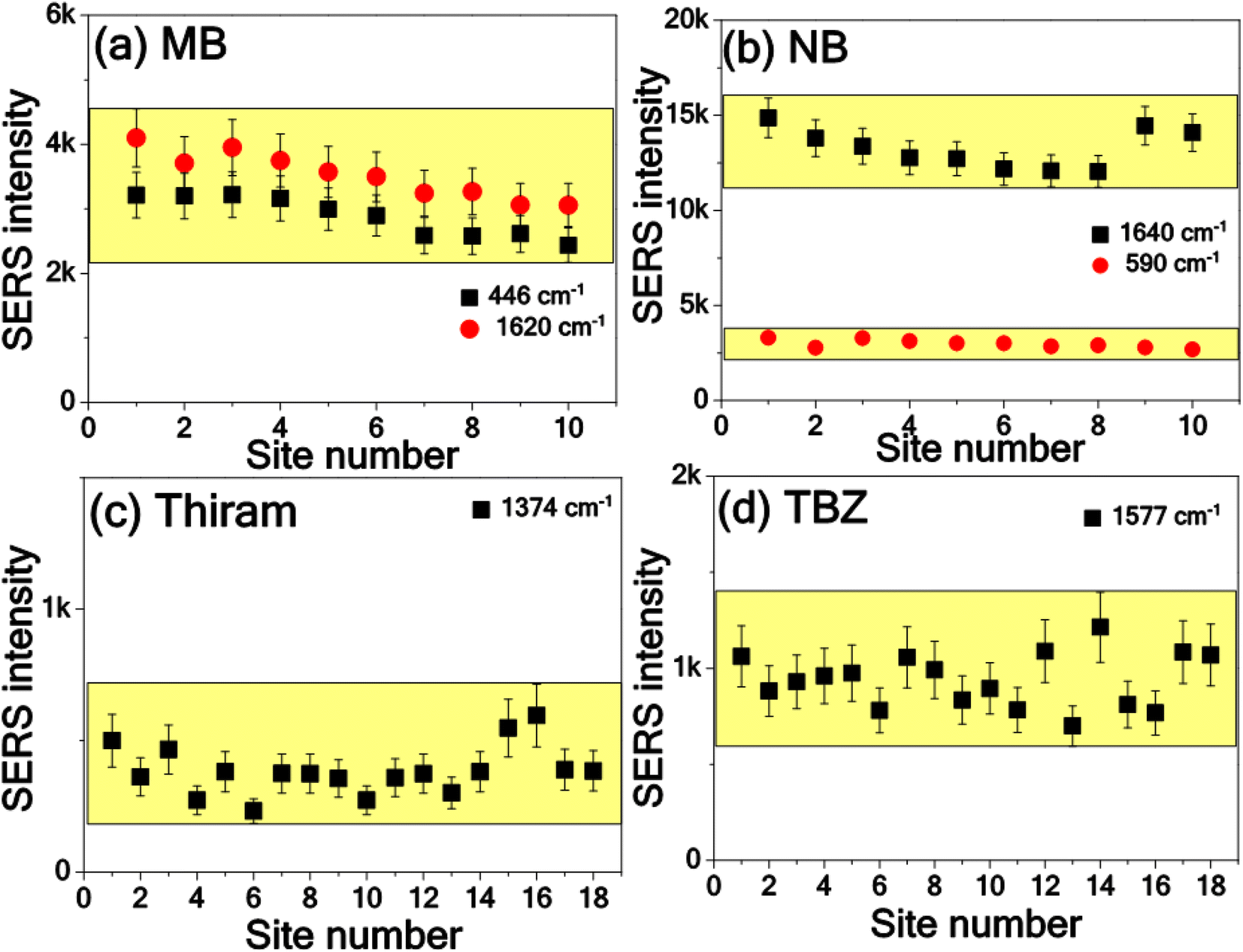 | ||
| Fig. 10 SERS intensity variation with analyte molecule in the mixed solution at different locations on Si_0.5C with Au nanostars (a and b) MB + NB (c and d) thiram + TBZ. | ||
Furthermore, well-established COMSOL Multiphysics (version 5.4 a, wave optics module) simulations were performed in order to calculate the electromagnetic field distribution around the Au nanostars. The perfectly matched layers (PMLs) absorb stray radiation, the mesh size of 0.2 nm, and the excitation of wavelength ∼785 nm in an X-polarized wave. All the material refractive indices used in this simulation are collected from previous studies.44,45 Fig. 11(a) represents the electric field distribution of a single Au nanostar with ∼50 μm core and eight tips. The tips of the Au nanostars in the direction of the applied electric field exhibit significant field enhancement than the other locations. Furthermore, simulations are also conducted for two Au stars (array of Au nanostars) separated by 1 nm in air, shown in Fig. 11(b). If two or more NPs are close to each other, there is a maximum electric field of up to 9 V m−1 compared to a single Au nanostar in the air (EM-field up to 6 V m−1). Additionally, simulations were also performed on the Au nanostars deposited SiO2 substrate. The maximum EM-field enhancement was noticed and was increased up to 231 V m−1 when the two Au nanostars with 1 nm separation were supported on a SiO2 substrate. The maximum electric field locations provide a higher number of hot spots along with the charge transfer possibility enhance the Raman signal of the probe molecules. These theoretical results further confirmed the Au stars decorated SiO2 features offer higher EM-field enhancement, which led to the observation of higher Raman enhancement for the probe molecules.
 | ||
| Fig. 11 COMSOL Multiphysics simulations of (a) a single Au nanostar in air medium, (b) two Au nanostars separated by 1 nm in the air, (c) two Au nanostars separated by 3 nm on SiO2 substrate. Wavelength of incident laser (785 nm) polarization direction along the x-axis. The color bar from blue to red represents the electric field intensity from weak to strong. | ||
Conclusions
In this report we have successfully demonstrated the fabrication of Au nanostars embedded fs laser-patterned Si hybrid SERS substrates for the detection of pesticides, dye, and their mixtures at ppm and ppb level concentrations. Initially, various nano-dimensional features on Si substrates were obtained by tuning the laser parameters (pulse numbers). These Si nano surfaces were decorated with Au nanostars achieved with chemical routes. The Au nanostars embedded laser-patterned Si surfaces provided additional SERS enhancements as compared to the Au nanostars embedded plain Si substrate. It is worth mentioning that the Au nanostars embedded laser-patterned Si (denoted with Si_0.5C) offered the best SERS performance than other laser-patterned Si substrates as well as “two order of Raman enhancement” compared to the plain Si substrate. Additionally, better enhancement and acceptable reproducibility were attained for the Si_0.5C SERS substrate, among the others. Furthermore, MB + NB and thiram + TBZ mixture compounds detection at ppm level using Si_0.5C was demonstrated with good sensitivity and reproducibility. The results obtained in this study could provide a pathway to detect mixed pesticide residues using nanostars decorated patterned substrates combined with a portable/handheld Raman spectrometer for real-time applications.Conflicts of interest
There are no conflicts to declare.Acknowledgements
We thank the University of Hyderabad for support through the Institute of Eminence (IoE) project UOH/IOE/RC1/RC1-2016. The IoE grant was obtained vide notification F11/9/2019-U3(A) from the MHRD, India. We acknowledge the School of Physics, UoH, for the FESEM characterization and XRD facilities. And also acknowledge Ms. Tania K. Naqvi, IIT Kanpur, for the AFM facility. The authors thank Director, ACRHEM for his encouragement and support during various fruitful discussions.References
- S. Weng, X. Hu, J. Wang, L. Tang, P. Li, S. Zheng, L. Zheng, L. Huang and Z. Xin, J. Agric. Food Chem., 2021, 69, 2950–2964 CrossRef CAS PubMed.
- N. H. Anh, M. Q. Doan, N. X. Dinh, T. Q. Huy, D. Q. Tri, L. T. Ngoc Loan, B. Van Hao and A. T. Le, RSC Adv., 2022, 12, 10950–10988 RSC.
- R. Zamora Sequeira, R. Starbird Pérez, O. Rojas Carillo and S. Vargas Villalobos, Molecules, 2019, 24, 2659 CrossRef CAS PubMed.
- I. B. Becerril-Castro, I. Calderon, N. Pazos-Perez, L. Guerrini, F. Schulz, N. Feliu, I. Chakraborty, V. Giannini, W. J. Parak and R. A. Alvarez-Puebla, Analysis Sensing, 2022, 2, e202200005 CrossRef CAS.
- J. Krajczewski, K. Kołątaj and A. Kudelski, RSC Adv., 2017, 7, 17559–17576 RSC.
- J. Krajczewski, A. Michałowska and A. Kudelski, Spectrochim. Acta, Part A, 2020, 225, 117469 CrossRef CAS PubMed.
- A. Shiohara, S. M. Novikov, D. M. Solís, J. M. Taboada, F. Obelleiro and L. M. Liz-Marzán, J. Phys. Chem. C, 2015, 119, 10836–10843 CrossRef CAS.
- V. O. Yukhymchuk, O. M. Hreshchuk, V. M. Dzhagan, M. V. Sakhno, M. A. Skoryk, S. R. Lavoryk, G. Y. Rudko, N. A. Matveevskaya, T. G. Beynik and M. Y. Valakh, Phys. Status Solidi B, 2018, 1800280 Search PubMed.
- C. Hrelescu, T. K. Sau, A. L. Rogach, F. Jäckel and J. Feldmann, Appl. Phys. Lett., 2009, 94, 153113 CrossRef.
- S. Park, J. Lee and H. Ko, ACS Appl. Mater. Interfaces, 2017, 9, 44088–44095 CrossRef CAS PubMed.
- T. H. Chang, Y.-C. Chang, C. M. Chen, K.-W. Chuang and C. M. Chou, J. Alloys Compd., 2019, 782, 887–892 CrossRef CAS.
- T. Chung and S.-H. Lee, Plasmonics, 2022, 1–9 Search PubMed.
- A. Guerrero-Martínez, S. Barbosa, I. Pastoriza Santos and L. M. Liz Marzán, Curr. Opin. Colloid Interface Sci., 2011, 16, 118–127 CrossRef.
- R. Wu, Q. Jin, C. Storey, J. Collins, G. Gomard, U. Lemmer, L. Canham, R. Kling and A. Kaplan, Nanoscale Horiz., 2021, 6, 781–790 RSC.
- H. S. Kang, M. Y. Long, T. Zhou, J.-C. Liu, Y. T. Duan, L. Ma, X. B. Chen, S. J. Ding and L. Zhou, J. Mater. Chem. C, 2022, 10, 958–968 RSC.
- J. F. Betz, W. W. Yu, Y. Cheng, I. M. White and G. W. Rubloff, Phys. Chem. Chem. Phys., 2014, 16, 2224–2239 RSC.
- Y. Yan, J. Zhang, P. Xu and P. Miao, RSC Adv., 2017, 7, 11969–11978 RSC.
- V. S. Vendamani, S. V. S. N. Rao, A. P. Pathak and V. R. Soma, ACS Appl. Nano Mater., 2022, 5, 4550–4582 CrossRef CAS.
- P. Mandal and B. S. Tewari, Surf. Interfaces, 2022, 28, 101655 CrossRef CAS.
- J. S. Jo, J. Choi, S. H. Lee, C. Song, H. Noh and J. W. Jang, Small, 2021, 17, 2005036 CrossRef CAS PubMed.
- T. D. Tran, T. H. Nguyen and T. B. Nguyen, J. Raman Spectrosc., 2022, 53, 1039–1047 CrossRef CAS.
- D. Zhang, B. Gökce and S. Barcikowski, Chem. Rev., 2017, 117, 3990–4103 CrossRef CAS PubMed.
- S. S. B. Moram, A. K. Shaik, C. Byram, S. Hamad and V. R. Soma, Anal. Chim. Acta, 2019, 1101, 157–168 CrossRef PubMed.
- C. Byram, S. S. B. Moram, A. K. Shaik and V. R. Soma, Chem. Phys. Lett., 2017, 685, 103–107 CrossRef CAS.
- M. Sree Satya Bharati, C. Byram and V. R. Soma, Front. Phys., 2018, 6, 28 CrossRef.
- S. Hamad, S. S. Bharati Moram, B. Yendeti, G. K. Podagatlapalli, S. Nageswara Rao, A. P. Pathak, M. A. Mohiddon and V. R. Soma, ACS Omega, 2018, 3, 18420–18432 CrossRef CAS PubMed.
- X. Wang, W. Shi, G. She and L. Mu, J. Am. Chem. Soc., 2011, 133, 16518–16523 CrossRef CAS PubMed.
- J. A. Powell, K. Venkatakrishnan and B. Tan, Sci. Rep., 2016, 6, 1–13 CrossRef PubMed.
- L. Cao, B. Nabet and J. E. Spanier, Phys. Rev. Lett., 2006, 96, 157402 CrossRef PubMed.
- S. M. Wells, I. A. Merkulov, I. I. Kravchenko, N. V. Lavrik and M. J. Sepaniak, ACS Nano, 2012, 6, 2948–2959 CrossRef CAS PubMed.
- K. Nehra, S. K. Pandian, M. S. S. Bharati and V. R. Soma, New J. Chem., 2019, 43, 3835–3847 RSC.
- F. Liang and R. Vallée, Opt. Mater. Express, 2016, 6, 3330–3338 CrossRef CAS.
- T. Chen, W. Wang, T. Tao, A. Pan and X. Mei, Appl. Surf. Sci., 2020, 509, 145182 CrossRef CAS.
- M. V. Shugaev, C. Wu, O. Armbruster, A. Naghilou, N. Brouwer, D. S. Ivanov, T. J.-Y. Derrien, N. M. Bulgakova, W. Kautek and B. Rethfeld, MRS Bull., 2016, 41, 960–968 CrossRef.
- P. Pellacani, V. Torres-Costa, F. Agulló-Rueda, R. Vanna, C. Morasso and M. Manso Silván, Colloids Surf., B, 2019, 174, 174–180 CrossRef CAS PubMed.
- I. A. Movtchan, R. W. Dreyfus, W. Marine, M. Sentis, M. Autric, G. Le Lay and N. Merk, Thin Solid Films, 1995, 255, 286–289 CrossRef CAS.
- S. S. B. Moram, C. Byram, S. N. Shibu, B. M. Chilukamarri and V. R. Soma, ACS Omega, 2018, 3, 8190–8201 CrossRef CAS PubMed.
- T. H. Chang, K.-W. Chuang, Y. C. Chang and C. M. Chou, Mater. Chem. Phys., 2022, 280, 125823 CrossRef CAS.
- X. Tan, L. Jiang, J. Hu, P. Liu, A. Wang and Y. Lu, Chin. Opt. Lett., 2015, 13, 111401 CrossRef.
- J. Rathod, C. Byram, R. K. Kanaka, M. Sree Satya Bharati, D. Banerjee, M. Akkanaboina and V. R. Soma, ACS Omega, 2022, 15969–15981 CrossRef CAS PubMed.
- B. Chandu, M. Bharati and S. V. Rao, IEEE Workshop on Recent Advances in Photonics, WRAP, 2017, pp. 1–3, DOI:10.1109/WRAP.2017.8468553.
- F. K. Alsammarraie, M. Lin, A. Mustapha, H. Lin, X. Chen, Y. Chen, H. Wang and M. Huang, Food Chem., 2018, 259, 219–225 CrossRef CAS PubMed.
- H. Sun, H. Liu and Y. Wu, Appl. Surf. Sci., 2017, 416, 704–709 CrossRef CAS.
- E. D. Palik, Handbook of optical constants of solids, Academic press, 1998 Search PubMed.
- D. E. Aspnes and A. A. Studna, Phys. Rev. B: Condens. Matter Mater. Phys., 1983, 27, 985–1009 CrossRef CAS.
Footnote |
| † Electronic supplementary information (ESI) available. See DOI: https://doi.org/10.1039/d2ra07859g |
| This journal is © The Royal Society of Chemistry 2023 |