
 Open Access Article
 This Open Access Article is licensed under a Creative Commons Attribution-Non Commercial 3.0 Unported Licence
Effect of vacancy defects on the electronic and mechanical properties of two-dimensional MoSi2N4
Ankan Ghosh Dastider a,
Ashiqur Rasula,
Ehsanur Rahmanb and
Md. Kawsar Alam*a
a,
Ashiqur Rasula,
Ehsanur Rahmanb and
Md. Kawsar Alam*a
aDepartment of Electrical and Electronic Engineering, Bangladesh University of Engineering and Technology, Dhaka 1205, Bangladesh. E-mail: kawsaralam@eee.buet.ac.bd; kawsar.alam@alumni.ubc.ca
bDepartment of Electrical and Computer Engineering, University of British Columbia, Vancouver, BC V6T 1Z4, Canada
First published on 10th February 2023
Abstract
MoSi2N4 is a recently fabricated 2-dimensional indirect bandgap semiconductor material that has attracted interest in various fields due to its promising properties. A defect-based thorough and reliable investigation of its physical properties is indispensable in this regard to explore its industrial applications in the future. In this work, a comprehensive vacancy defect-based analysis of the electronic and mechanical characteristics of this material is conducted with varying defect percentages. We have analyzed the gradual change in electronic properties of MoSi2N4 by performing first-principles density functional theory-based investigation and presented a detailed analysis for point vacancies ranging from 0.297% to 14.29%, revealing the transition of this monolayer from the semiconductor to metal phase. The gradual change in mechanical properties due to the defect introduction has also been reported and analyzed, where the Young's modulus, Poisson ratio, elastic constant, etc. are calculated by the stress–strain method using Matrix Sets (OHESS). Further, we extend the investigation to the exploration of thermal and topological characteristics and report the triviality of the MoSi2N4 material as well as the effect on specific heat, entropy, and free energy with respect to temperature. We believe that the results presented in this study could assist the process of incorporating MoSi2N4 in future 2D electronics.
1. Introduction
Isolating thin layers of materials from their 3-dimensional bulk parent compounds has been the center of attraction since the discovery of monolayer graphene back in 2004 which was a milestone for future research on 2D materials.1 Tremendous interest in this field led to the discovery of many other 2D materials like transition metal dichalcogenides (TMD), transition metal nitrides (TMNs), phosphorene, hexagonal boron nitride, etc.2–4 Very recently, in 2020, a novel 2D material MoSi2N4 has been synthesized using the chemical vapor deposition (CVD) method in a Cu/Mo bilayer substrate.5 In addition, the study used first-principles density functional theory (DFT) to compute the electronic characteristics of the synthesized compound. DFT-predicted more general XY2M4 materials (X = W, V, Nb, Ta, Ti, Zr, Hf, Cr; Y = Si, Ge; M = N, P, As) that emerged later on.6–11 The structure of MoSi2N4 is composed of a MoN2 monolayer sandwiched between two Si–N bilayers. It is an indirect bandgap material with a bandgap of 1.94 eV. The intrinsic electron and hole mobilities are predicted to be 270 cm2 V−1 s−1 and 1200 V−1 s−1, respectively,5 which are notably greater than those of previous 2D materials like MoS2. The discovery of new material like this one having exciting properties calls for various sorts of analysis to check its applicability in relevant fields.Various types of contact-based analysis and bandgap engineering-based methods have been investigated on this material.6,12,13 Structural defects like vacancies are almost unavoidable during the fabrication process or synthesis of 2D materials.14–18 These inevitable defects appear in various forms regardless of the level of precision of synthesis. Defect analysis in this kind of material is therefore an imperative task that plays an important role in determining the electronic, mechanical, magnetic, and many other properties. Defects can enforce localized electronic properties, changing swiftly from the 2D material themselves, let alone their 3D parent compounds. However, in the literature, there exists a lack of analysis on the characteristics of MoSi2N4 in the presence of vacancies. In ref. 19, ab initio calculation-based analysis is presented on the basis of the chemisorption of F-, H- and O-atoms on the MoSi2N4 monolayer along with substitutional doping by As, F, Ge, O, and P atoms in the low concentration range, and vacancy defects by removing single N, Si, or both atoms. All defects are reported to decrease the MoSi2N4 monolayer bandgap. In ref. 20, the authors reported that the N and Si vacancies generate magnetic moments, introducing half-metallicity in this compound. However, these studies didn't present thorough and successive transitions in the characteristics of this material due to the presence of various amounts of defects. Considering the real-life scenario where these types of vacancies are likely to be detected, it is quite imperative to comprehend the electronic characteristics of these vacancies. This type of analysis is also essential to pave the way for high-performance nanoelectronic devices.
Vacancies, a special form of defect, can be categorized into various classes; such as point vacancy, bi-vacancy, edge vacancy, and a mixture of all these. However, vacancy defect is the most common and abundant defect in some 2D materials like the TMDs.21 In this study, we have analyzed the gradual change in electronic properties of MoSi2N4 due to various vacancy levels in monolayer MoSi2N4 performing first-principles DFT investigation. Following the estimation of formation energy present in the literature to understand stability, we put emphasis on the point vacancies ranging from 14.29% to as low as 0.279%. The gradual change in mechanical properties due to the defect introduction has also been reported. For these varying scenarios, Young's modulus, Poisson ratio, elastic constant, etc. are calculated by the stress–strain method using Matrix Sets (OHESS). The relevant results are compared with the existing experimental ones for benchmarking and extended covering a variety of parameters with their analysis. In addition, as part of our routine study, we report the thermal properties and demonstrate the topological triviality of this material. Detailed computational details are presented for each of the calculations. This study demonstrates some exciting properties of this material and their semiconductor-to-metal alterations, mechanical behaviors, and their transitions which may contribute to the future applications of this material.
2. Computational details
DFT-based first-principle calculations22,23 presented in this study are performed using Vienna Ab initio Simulation Package (VASP).24,25 The plane-wave basis projector augmented wave (PAW) method26,27 is used along with the generalized gradient approximation (GGA) with Perdew–Burke–Ernzerhof (PBE) functional.28 The DFT-D3 method of Grimme29 was followed to hold the presence of the weak van der Waals (vdW) forces. The kinetic energy cut-off was set to 520 eV. The automatic k-mesh is used in the gamma-centered Brillouin zone with grids of 12 × 12 × 1 for the geometric optimizations and 30 × 30 × 1 for electronic calculations. The convergence criteria for electronic and ionic relaxations are set to 10−6 eV and 10−5 eV Å−1, respectively. In order to avoid any interaction between two neighboring layers, a 25 Å vacuum was kept in the z-direction. It is to be noted that in our calculations, generally a more accurate hybrid DFT using the Heyd–Scuseria–Ernzerhof (HSE) functional is not used. The reason behind this is the overestimation of bandgap using the HSE functional reported widely in the literature for these structures while the PBE functional gives a closer approximation to experimental data.5,13 The strongly constrained and appropriately normed (SCAN)30 meta-GGA functional provided the same bandgap and band structure as the GGA one. It is to be noted that some new exchange-correlation potentials proposed in the recent literature (e.g., LMBJ,31 TASK,32 and mTASK33 meta-GGA functionals) which may have potential applications in the future for a better manifestation of 2D semiconducting and semi-metallic systems.34,35The top and side views of a monolayer MoSi2N4, along with its band structure are shown in Fig. 1. The optimized lattice constant of this structure is MoSi2N4 is a = b = 2.91 Å. It is a hexagonal structure with a space group of P6m1. The DFT-calculated indirect bandgap is found to be 1.74 eV, which matches perfectly with the literature.5,13
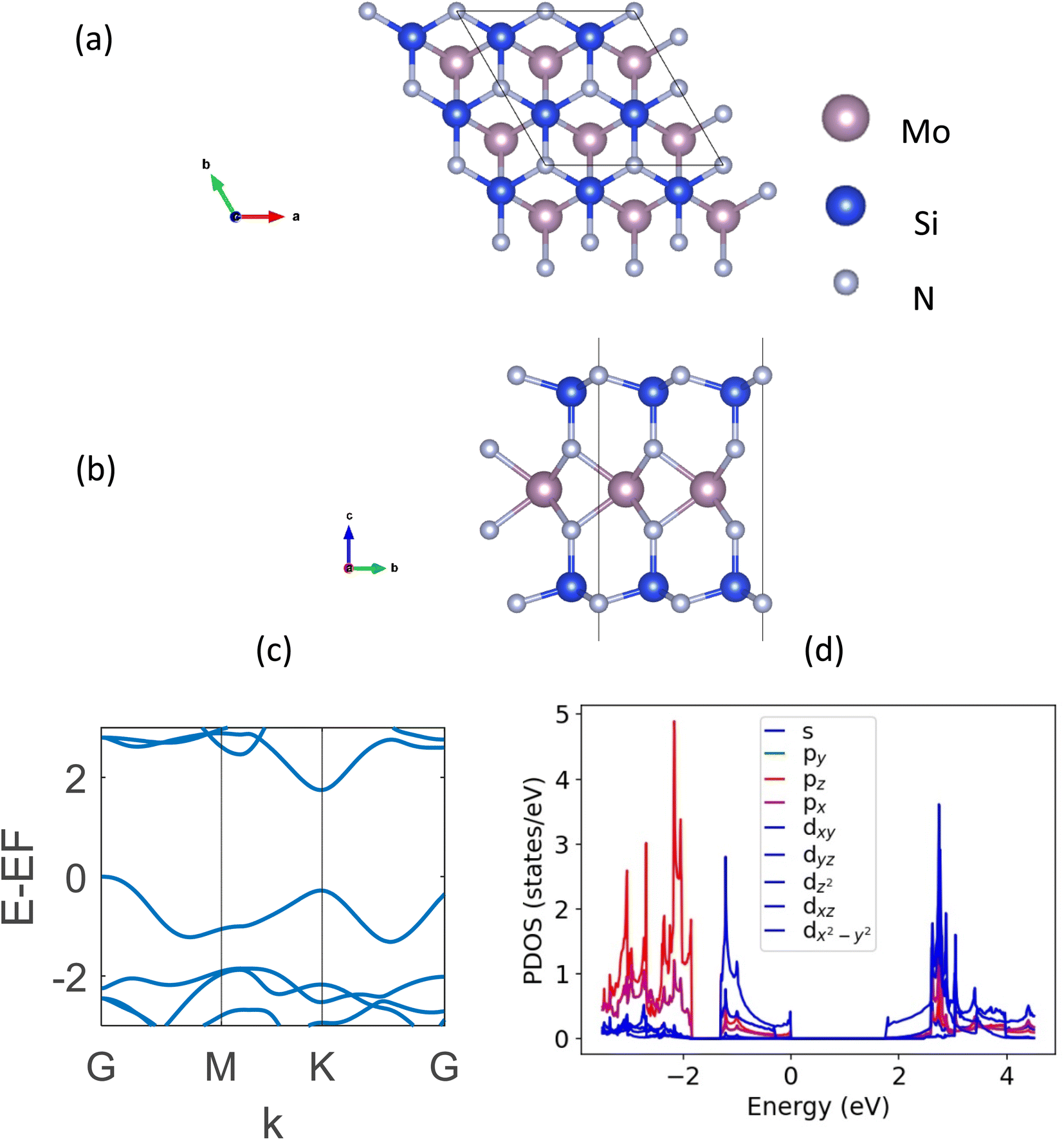 | ||
| Fig. 1 (a) Topview, (b) sideview, (c) DFT-calculated band structure, and (d) PDOS plot of monolayer MoSi2N4. | ||
Elastools36 was used to study the mechanical and elastic properties of the material. The stress–strain method is adapted for the accurate determination of characteristics and optimized for a high-efficiency strain matrix set. For obtaining the accurate phonon band structure and thermal properties, Phonopy37 is used, that adopts the finite displacement method to calculate phonon structure. This method requires the generation of a supercell in the range of 15–20 Å. We created a supercell of 4 × 4 × 1 to fulfill the requirement and after successful relaxation, symmetry resolving produces finite atomic displacement configurations. Self-consistent field calculation is performed on each of the 14 atomic displacement configurations and their output is used to produce the force constants of the material. For inspecting the topological characteristics, Wannier90 (ref. 38) code is applied in the library model to generate the maximally localized Wannier functions and WannierTools39 is used for further processing.
3. Results and discussion
Point vacancy is a special type of vacancy defect where an atom disappears from the lattice in a random manner. In this study, for the vacancy defect analysis of MoSi2N4, we have considered varying percentages of Si-vacancy (VSi) and N-vacancy in the Si–N layer (VN or VNout). N-vacancy in the MoN2 layer, represented as VNin, isn't considered due to their high formation energy than the ones used in this study. Therefore, VSi and VN vacancies are comparatively the most likely vacancies to appear, as the more probable structure holds low formation energy.19,20 It is proved in ref. 20 that VN is the most likely vacancy to appear in the structure, followed by the VSi. VMo, on the other hand, is unlikely to appear and therefore has not been considered in this study.The defect percentages are varied and the material properties for these different percentages are calculated accordingly. An atom is removed from the cells to create a vacancy inside them, as shown in Fig. 2, where one of such combinations is presented. Here we have incorporated a 1.58% defect by eliminating one Si atom from the 3 × 3 × 1 supercell. Removing an atom from the unit cell results in a 14.286% defect. Similarly, for the 221 cell, the defect level becomes 3.571%. Defect of 14.286% is not a realistic value, but in this study, we created defects in up to a 771 supercell, resulting in as little as 0.292% defects. It is to be noted that increasing cell size heightens the computational time exponentially. For example, with a configuration of 36 G RAM, P100 Pascal GPU, the total CPU time is 5669.465 s for the unit cell (6 atoms), 10![[thin space (1/6-em)]](https://www.rsc.org/images/entities/char_2009.gif) 591.838 s for the 221 supercells (27 atoms), and 48811.586 s for the 331 supercell (62 atoms).
591.838 s for the 221 supercells (27 atoms), and 48811.586 s for the 331 supercell (62 atoms).
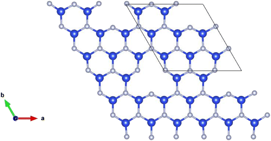 | ||
| Fig. 2 Schematic representation of a MoSi2N4-331 supercell with Si-vacancy defect. For visualization, only the defected Si–N layer is presented. | ||
3.1 Transition in metallic behavior
In this study, the electronic property of MoSi2N4 is calculated in a comprehensive way with varying vacancy percentages. In order to capture the results with a low level of defects, larger and larger cells were created. In the ESI materials of ref. 40, the authors demonstrated a total of 30 structures of MoSi2N4. The study used α and β phases of the two Si–N layers, and the 2H and 1T phases for the MoN2 layer. The different phases of MoN2 layer was sandwiched between the different phases Si–N layers to create these different combinations. We incorporated VN, the most likely defect, on six of them: α-1, α-2, α-3, α-4, β-1, and β-2. The band structure of each of the six structures with and without defects is presented in Fig. 3. It is evident that for each of them, there is a transition to metallic behavior due to the presence of VN. It is to be noted here that α-1 is the most probable structure among all.40 The result is presented in Table 1. | ||
| Fig. 3 (a)–(f) Band structure of six different structures of monolayer MoSi2N4 with and without VN. It is apparent that the vacancy defect leads to overlapping valence and conduction bands for all these structures. The observed states and bandgaps are presented in Table 1. | ||
| Phase | Bandgap (eV) or state | |
|---|---|---|
| Without vacancy | With VN | |
| α-1 | 1.731 | Metallic |
| α-2 | 0.013 | Metallic |
| α-3 | 0.206 | Metallic |
| α-4 | Metallic | Metallic |
| β-1 | Metallic | Metallic |
| β-2 | Metallic | Metallic |
Next, a detailed analysis of the change in metallic behavior of MoSi2N4 due to the presence of various amounts of defect percentages is performed. We considered 14.29%, 3.57%, 1.59%, 0.571%, and 0.292% of defects by eliminating a Nitrogen atom from 111 (unit cell), 221, 331, 551, and 771 supercells, respectively. As larger supercells are required to reduce the defect percentage, the computational expense increases manifold. The acquired band structures of these calculations, along with their corresponding Projected Density of States (PDOS) plots, are presented in Fig. 4.
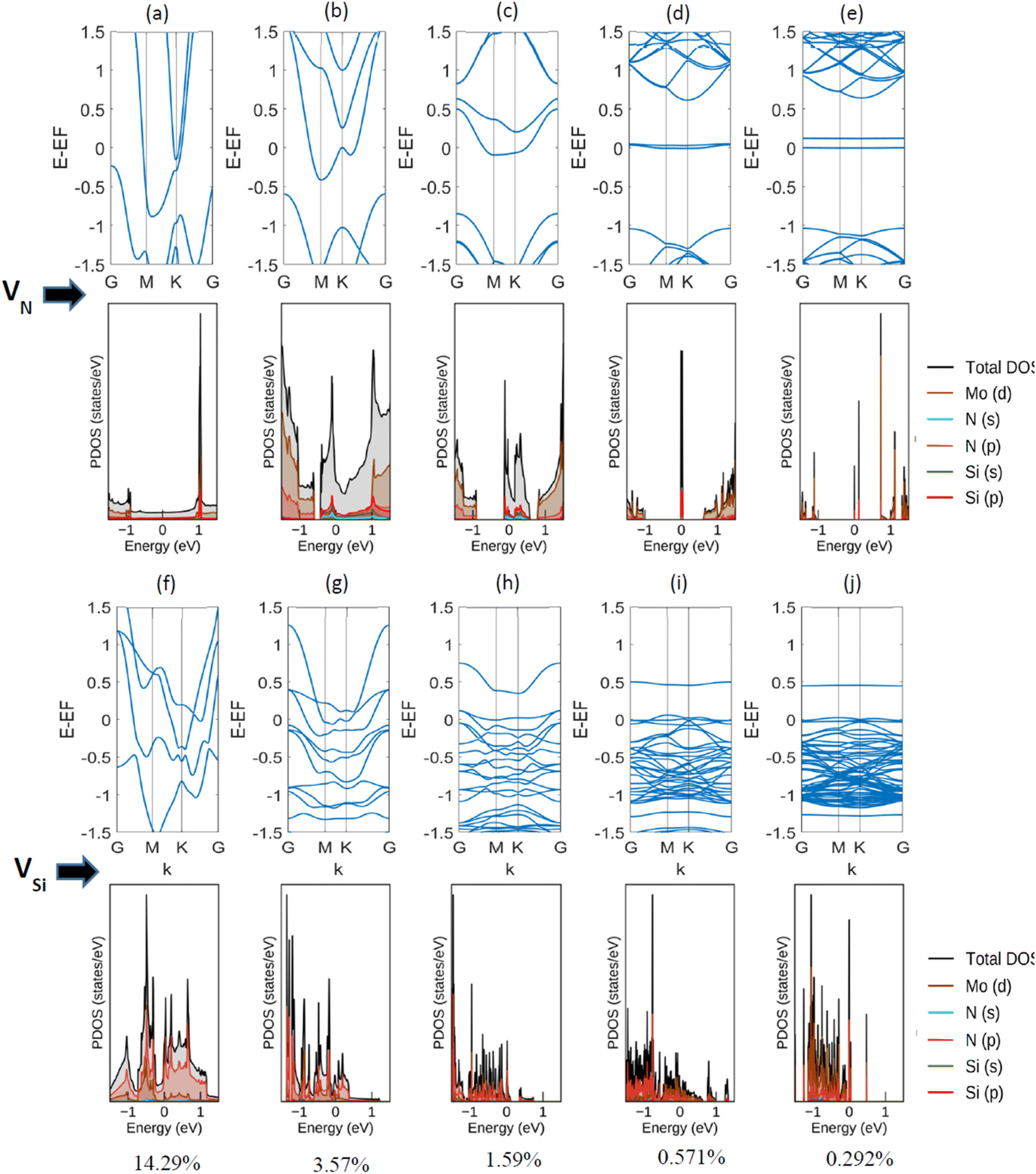 | ||
| Fig. 4 Band structures and projected density of states (PDOS) of α-1 MoSi2N4 monolayer with different (a)–(e) N and (f)–(j) Si-defect percentages. For VN, the metallic to semi-metallic transition is observed at around (d) 0.571% defect, whereas the same is noted in VSi for around (j) 0.292% defect. Plotted in −1.5 to 1.5 scale for better visualization. | ||
We observe here that as the vacancy percentages decrease, there is a clear transition in the metallic behavior of this material. For the highest percentage (14.29%, created by reducing a single N-atom from the Si–N layer of a unit cell), there is a clear overlapping region of conduction and valence band, apart from having a Fermi-level crossing. As the percentages decrease, a gap between the conduction and valence bands starts to appear, but the Fermi-level crossing is still present. For Si, on the other hand, the overlapping region of conduction and valence band exists before 0.292% (created by reducing a single N-atom from the Si–N layer of a 771 supercell). We note a semi-metallic behavior at this amount of vacancy. The summary of the obtained result is shown in Table 2.
| Percentages (%) | State | |
|---|---|---|
| For VN | For VSi | |
| 14.286 | Metallic | Metallic |
| 3.571 | Metallic | Metallic |
| 1.587 | Metallic | Metallic |
| 0.571 | Semi-metallic | Metallic |
| 0.292 | Semi-metallic | Semi-metallic |
3.2 Mechanical properties
Mechanical characteristics of materials are not only essential variables in their application sectors, but they are also crucial in terms of materials science and material creation. Since the successful creation of graphene with an atomic thickness, 2D materials have gotten a lot of interest because of their unique features, especially their remarkable mechanical qualities like high Young's modulus and strength. Two separate parameters known as the equation of state and strength are typically used to explain a solid's reaction to a mechanical deforming process. The toughness of materials are generally calculated using the strain-energy technique or the stress–strain approach whereas the stress–strain approach, being more precise, is computationally more expensive.36Strain matrix sets are required for the computation of second-order elastic constants and their derivative characteristics.41 Elastool may use three distinct strain matrix sets: the optimal high-efficiency strain matrix set (OHESS),42 the universal linear independent coupling strains (ULILCS), and the all single element strain matrix set (ASESS).43 Although each has its own benefits and drawbacks, the optimal high-efficiency strain matrix set (OHESS) is best suited for calculating 2D materials with minimal strain levels and little processing effort.
The elastic constants of a material can be obtained from the relation between the stress σi and its induced strains  that is
 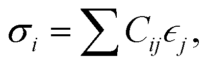 where strain
  is applied and corresponding stresses are calculated. The deformation matrix applied is expressed as:
 | (1) |
 is the strain matrix in Voigt notation. For a layered 2D material, the crystal plane is assumed to be in the XY plane and the strain matrix is:
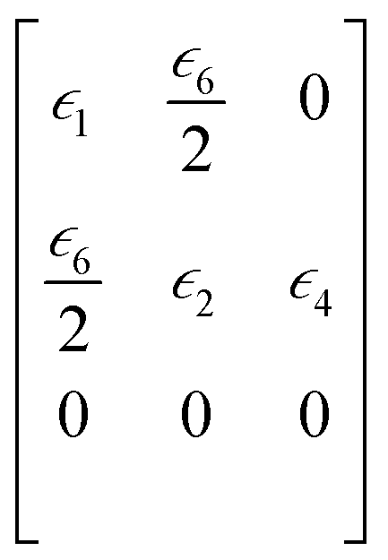 | (2) |
4 levels of strains: 0.6%, 0.3%, both as tensile and compressive, is applied as deformations to the relaxed structure. These structures then undergo self-consistent field calculation to determine the stress matrix.
Young's modulus and Poisson's ratio are calculated on the basis of the arithmetic average of the Voigt and Reuss bound44 by the following equations:
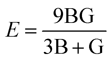 | (3) |
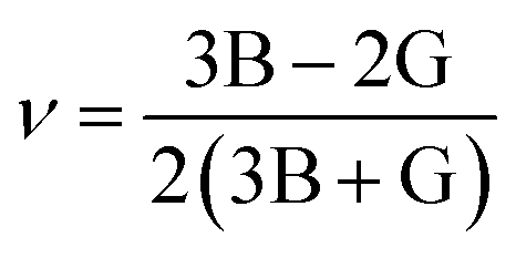 | (4) |
The phase velocity v and polarization of the 3 waves along a fixed propagation direction defined by the unit vector n are given by Christoffel equation as:45
| (Cijklnjnk − ρv2δij)uij = 0, | (5) |
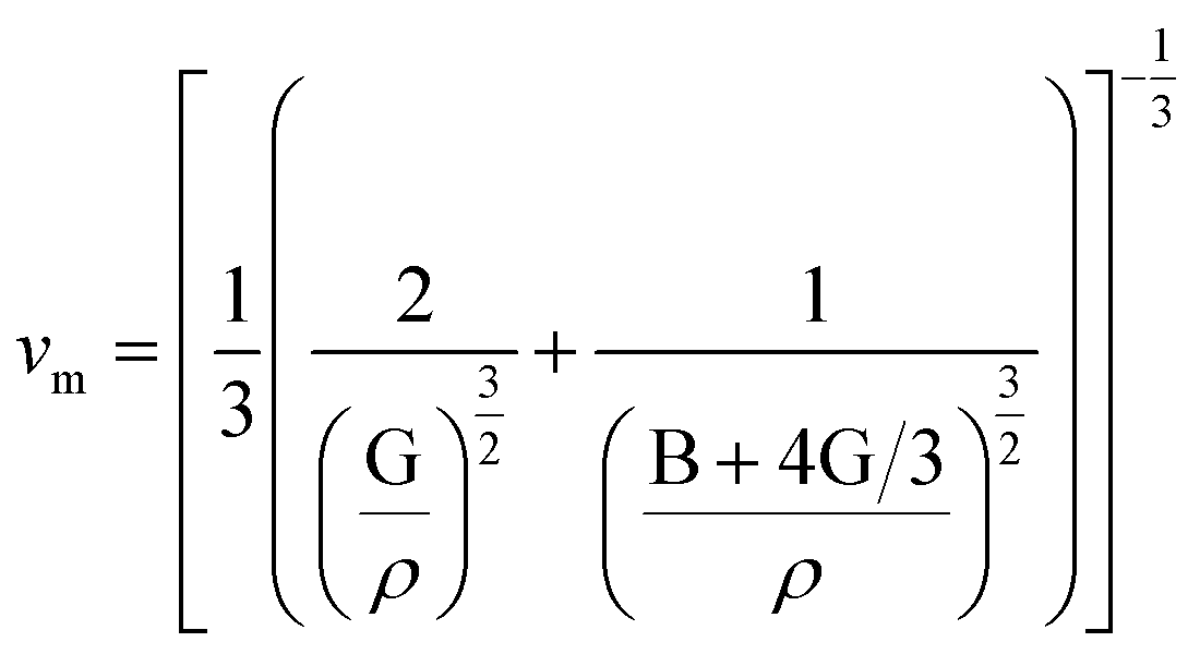 | (6) |
 is the longitudinal wave velocity and
  is the shear wave velocity. The Debye temperature is expressed as:
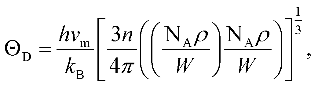 | (7) |
In this study, 11 different types of mechanical parameters are investigated with and without the appearance of N-vacancy defects. At first, the parameters are calculated for the defectless unit cell. Table 3 demonstrates the differences between experimental values and mechanical values calculated through the ab initio calculation method for Poisson ratio, elastic constants, and Young's modulus. It clearly shows that our calculated values closely match to the experimental ones. Also we note that MoSi2N4 has superior elastic properties compared to MoS2; Young's modulus is more than twice in MoSi2N4 than that of MoS2. The Poisson's ratio and elastic constants are also greater in MoSi2N4.
| Material | MoSi2N4 (ab initio calculation) | MoSi2N4 (experimental) | MoS2 |
|---|---|---|---|
| Poisson ratio | 0.28 | 0.28 (ref. 46) | 0.254 (ref. 47–49) |
| Elastic constant C11 (N m−1) | 540 | 539 (ref. 10) | 149.42 (ref. 48 and 49) |
| Elastic constant C12 (N m−1) | 151.64 | 152 (ref. 10) | 32.6 (ref. 48 and 49) |
| Young's modulus (GPa) | 497.55 | 491.4 ± 139.1 (ref. 5) | 270 ± 100 (ref. 47, 48 and 50) |
Next, we extended the calculation for all 11 parameters for cells with VN. We considered 4 cases with vacancy: from 0% to 4.762%. Table 4 lists the total number of elastic parameters that are determined from the study with varying defect levels. The mean pressure, elastic constant (C11, C12), Debye temperature, sound velocities (VLA, VSA, VMA), Young's modulus, shear modulus, bulk modulus, and Poisson ratio are reported here.
| Defect level | 0.000% | 1.580% | 2.381% | 3.570% | 4.762% |
|---|---|---|---|---|---|
| Mean pressure (GPa) | 0.10 | 0.27 | 0.32 | 0.05 | 0.05 |
| Elastic constant C11 (N m−1) | 540.14 | 513.5 | 504.19 | 454.88 | 481.60 |
| Elastic constant C12 (N m−1) | 151.64 | 191.23 | 188.89 | 164.09 | 158.38 |
| Debye temp. (K) | 1562.84 | 1431.4 | 1448.24 | 1350.6 | 1399.04 |
| VLA (km s−1) | 10.70 | 10.46 | 10.61 | 9.88 | 10.05 |
| VSA (km s−1) | 6.42 | 5.86 | 5.93 | 5.59 | 5.82 |
| VMA (km s−1) | 5.91 | 5.45 | 5.52 | 5.19 | 5.39 |
| Young's modulus (N m−1) | 497.55 | 442.28 | 455.23 | 395.68 | 420.29 |
| Shear modulus (N m−1) | 194.2 | 161.13 | 165.58 | 145.39 | 158.14 |
| Bulk modulus (N m−1) | 345.91 | 352.37 | 363.98 | 309.48 | 313.12 |
| Poisson ratio | 0.28 | 0.37 | 0.34 | 0.36 | 0.33 |
The Debye temperature corresponds to the elastic qualities with the thermodynamic properties, such as phonons, thermal expansion, thermal conductivity, specific heat, and lattice enthalpy.51 It provides a decent estimate for the low-temperature heat capacity of crystalline, insulating substances when other contributions (such as highly mobile conduction electrons) are insignificant. For metals, the electron contribution to heat is proportional to T, which dominates at low temperatures the Debye result for lattice vibrations, T3. In this instance, it can only be argued that the Debye model is approximate for the lattice contribution to the specific heat. It is also believed to hold a relationship with energy bandgap.52 In our calculations, we note that the temperature decreases with increasing defect levels, but it is not consistent. For the unit cell, the temperature is 1562.84 K, which reduces to 1350.6 K for a 3.57% defect percentage.
Poisson's ratio is another valuable indicator of how much a material deforms under stress (stretching or compression). It is imperative for mechanical engineering as it enables the selection of materials according to the required purpose. It is a crucial characteristic for describing the elastic deformation behavior of a material.53 Indeed, the enormous magnitude of programmable Poisson's ratio allows materials to exhibit shape-morphing capability and significantly enhanced mechanical characteristics, including strength, indentation resistance, fracture toughness, energy absorption, etc.54
Most materials have Poisson's ratio values ranging between 0.0 and 0.5, like the one used in this study. We note that the ratio always increases for the defect (>0.3) than the one for the unit cell. Therefore, we can tune the tensile compression of this material by introducing defects. The elastic constants are imperative parameters for analyzing the mechanical properties of materials, the other parameters are calculated based on these. The values of these constants deviate from their initial pristine monolayer value due to the appearance of vacancies, as apparent from Table 4. We also report several other parameters, which demonstrate the material's ability to alter its mechanical properties as a result of defect introduction.
The trend in different modulus values with the varying defect levels is presented in Fig. 5. We can note here that except for Young's modulus, other elastic properties remain constant with changing defect levels and all the structures with defects show mechanical stability. These structures of MoSi2N4 are mechanically stable if the Born stability criteria55,56 is satisfied. The Born stability criteria are defined as:
| C11 + 2C12 > 0, C44 > 0, C11 − C12 > 0 | (8) |
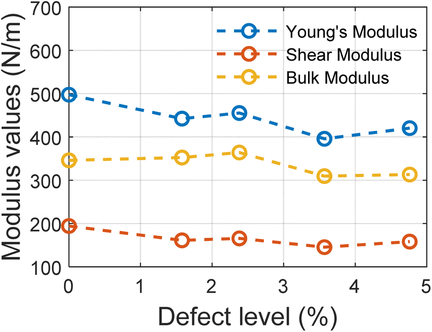 | ||
| Fig. 5 Variation in Young modulus, shear modulus, and bulk modulus with varying defect percentages. | ||
For all the structures, the required criteria are met. So these structures are mechanically stable ones.
3.3. Thermal properties
We expand our study towards the exploration of a few basic thermal properties of MoSi2N4. The phonon serves crucial roles in a variety of dynamical behaviors and thermal characteristics, both of which are fundamentally important aspects of material science. The energy E of a phonon system can be expressed as:37
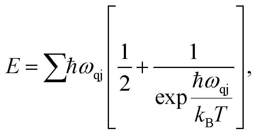 | (9) |
Fig. 6 shows the phonon band structure and phonon density of states calculated. In the plot, we note that there is no negative frequency component, which solidifies the claim of structural stability of MoSi2N4. These results perfectly match with the results available on ref. 5 and 57. Next, we calculated the thermal properties like free energy, entropy, and specific heat calculated for the MoSi2N4 monolayer (Fig. 7). We note that although free-energy decreases with increasing temperature, both entropy and Cv are increasing.
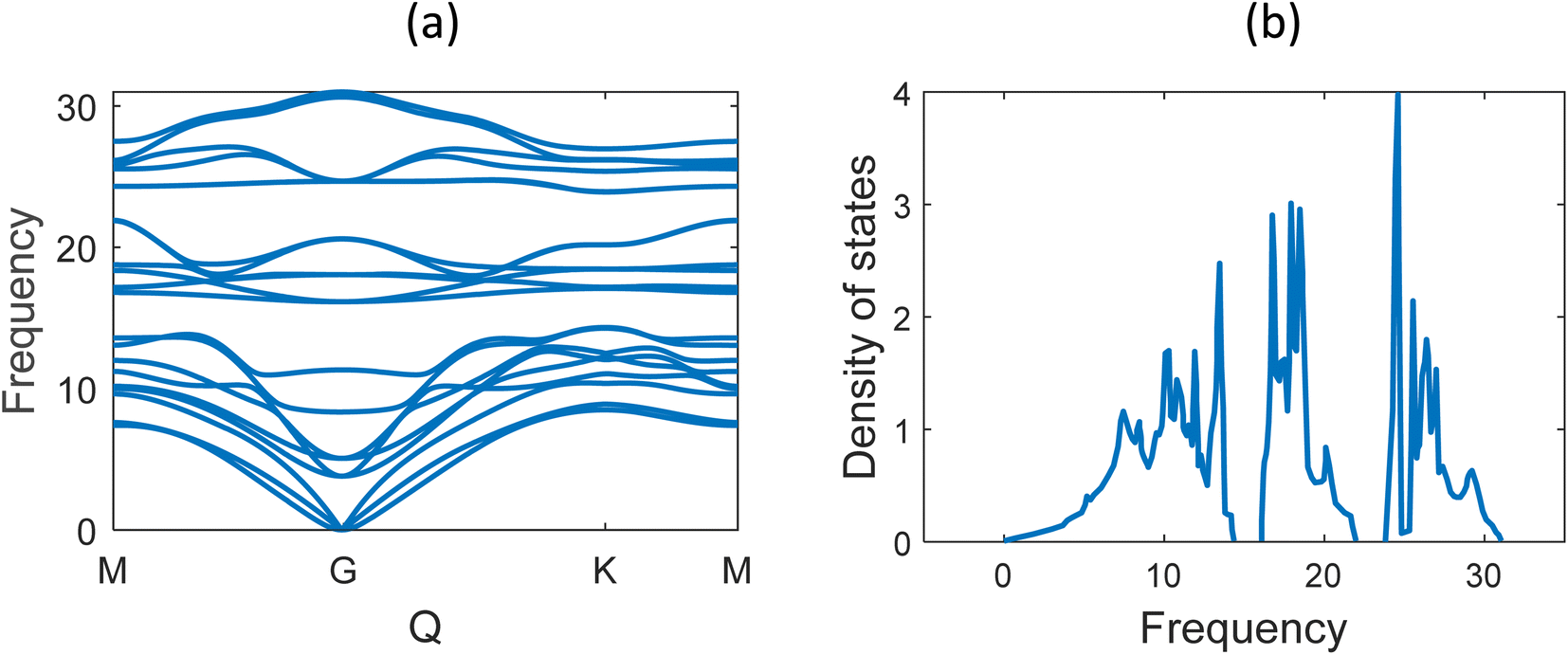 | ||
| Fig. 6 (a) Phonon band structure and (b) phonon density of states of MoSi2N4. | ||
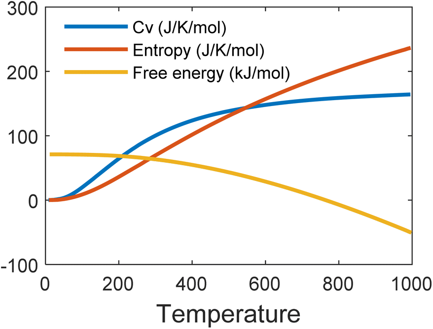 | ||
| Fig. 7 Free energy, entropy and specific heat of MoSi2N4 with respect to increasing temperature. | ||
3.4. Topological properties
Novel topological states have garnered considerable interest during the last several decades. Since the quantum spin hall effect (QSHE)58 was predicted in 2005 and realized in HgTe/CdTe quantum wells in 2007, an increasing number of topological novel states have been discovered, such as 3D topological insulators, Dirac,59 Weyl semimetals,60 Hourglass fermions,61 Nodal line semimetals,62 and nodal chain metals, etc. Currently, a large number of novel topological phases are developing, and an increasing number of materials are being recognized as topologically nontrivial. Therefore, we extend our analysis to explore the topological nature of MoSi2N4. For investigating these properties, the following projections were chosen: d orbital for the Mo atom, p orbital for the Si atom, and p orbital for the N atom. Thus a total of 23 Wannier centers are used with 140 bands for accurate calculation. The disentanglement window is set from −20 to 30 eV, and the frozen window is set from −11.5 to 4 eV with a total number of disentanglement iterations set as 1000 and convergence iteration as 20. Disentanglement and frozen windows are chosen from projected band structures of different atoms and their related orbitals to enclose the preferred band near the Fermi surface. In order to check the correctness of wannierization, Wannier interpolated band structure is plotted with the band path as K–G–M–K. We also incorporated spin–orbit coupling (SOC) in the calculations to consider spin interactions. In the WannierTools post-processing step, a 101 × 101 × 1 k points grid is used and the Fermi energy is set to −0.202 and projections in the conventional <010> direction. Fig. 8 shows the observed surface states of MoSi2N4 along with MoS2, another 2D material with auspicious properties, for a relative comparison. As we can observe, the later material has a Dirac cone in the Fermi level at the Gamma point, however, such a cone is not visible in the case of MoSi2N4. It is evident that MoSi2N4 is topologically trivial.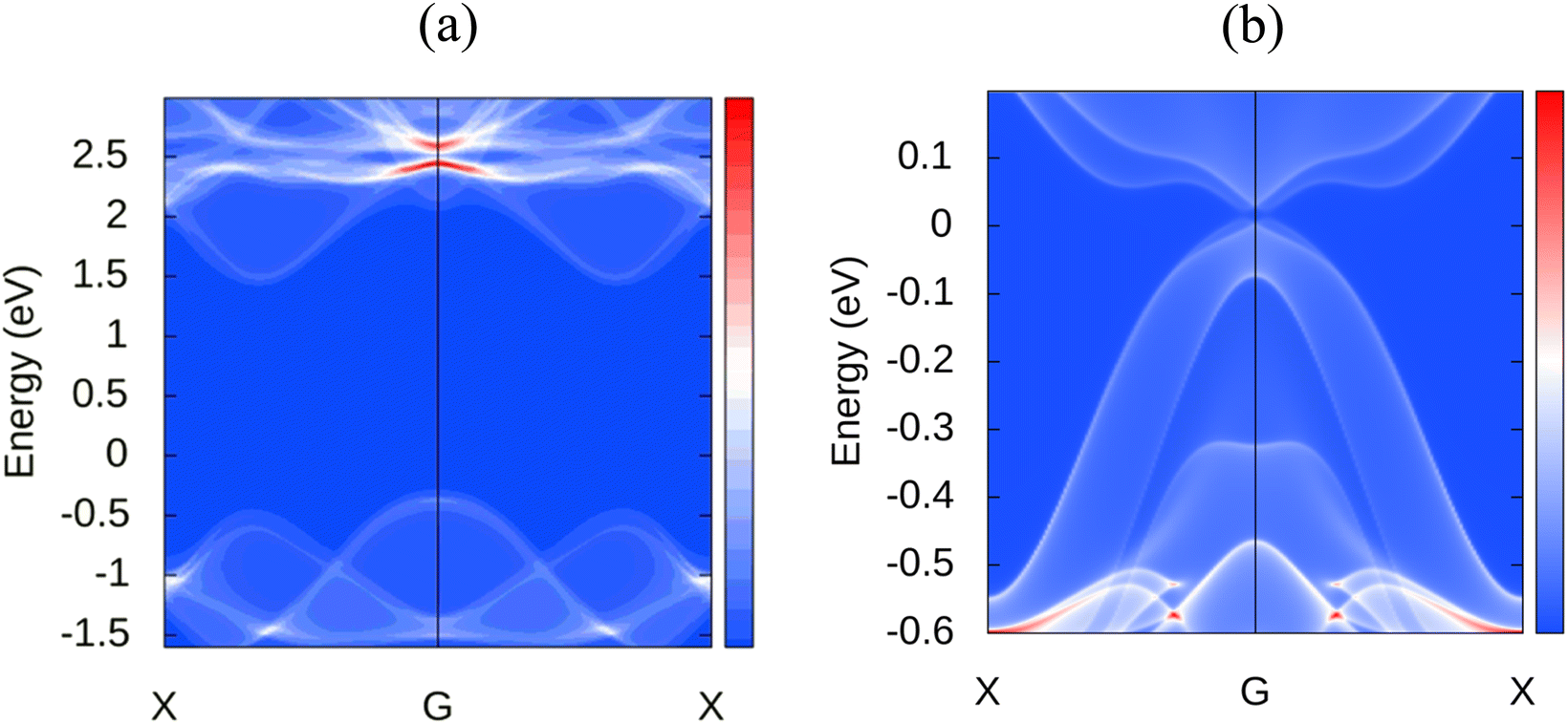 | ||
| Fig. 8 Surface states comparison between (a) MoSi2N4 and (b) MoS2. | ||
The Fermi velocity is another key parameter of a material, it contributes to the device characteristics as well. The Fermi velocity of MoSi2N4 is found to be 2.96 × 10⁶ m s−1, similar to the popular 2D material graphene which has a Fermi velocity up to 3 × 10⁶ m s−1.63
It is to be noted that in this study, we have focused on the effects of vacancy defects in the MoSi2N4's properties. There could be other types of defects in this material, including substitutional defects, dislocations, etc., manifesting different phenomena. The effect of the number of layers could also change the material properties. Defects in these novel structures could lead to other exciting fields of applications. However, these topics are out of the scope of this study and are some potential sector for future works.
4. Conclusion
In this work, we have reported a detailed analysis on various material properties of MoSi2N4 with a special focus on defect-based deviations on these properties. A comprehensive defect-based analysis of the monolayer of this material has been presented by varying the percentages of vacancy defects where the results display a clear transition from semiconductor to metallic behavior for a certain amount of defects. The mechanical properties of these materials demonstrated some deflections in the properties of this material due to the defects, which is revealed by exploring the elastic constant, Debye temperature, Young's modulus, shear modulus, bulk modulus, Poisson ratio, etc. It is found that all the structures with varying percentages of defects are mechanically stable. Thermal and topological properties were also inspected as part of routine analysis on this material, demonstrating the relation between free energy, entropy, and specific heat with respect to temperature and also the topological triviality of this material. Detailed computational details have been presented for each of the calculation. This work deals with some exciting properties of this material and their transitions in a more realistic way and therefore holds a high potential for future applications of this material.Author contributions
A. G. D. and A. R. initiated the research work presented here. The analysis has been performed by A. G. D., and A. R. with support from E. R., and M. K. A. A. G. D. prepared the draft with contributions from A. R., E. R., and M. K. A. The project has been supervised by M. K. A.Conflicts of interest
There are no conflicts of interest to declare.Acknowledgements
The authors would like to thank the Nanoscale Devices and Materials Research Laboratory, Bangladesh University of Engineering and Technology (BUET), for providing continuous computational support throughout the study.References
- K. S. Novoselov, A. K. Geim, S. V. Morozov, D. Jiang, Y. Zhang, S. V. Dubonos, I. V. Grigorieva and A. A. Firsov, Science, 2004, 306, 666–669 CrossRef CAS PubMed.
- A. Bafekry, M. Yagmurcukardes, B. Akgenc, M. Ghergherehchi and C. V. Nguyen, J. Phys. D: Appl. Phys., 2020, 53, 355106 CrossRef CAS.
- K. Huang, Z. Li, J. Lin, G. Han and P. Huang, Chem. Soc. Rev., 2018, 47, 5109–5124 RSC.
- L. H. Li and Y. Chen, Adv. Funct. Mater., 2016, 26, 2594–2608 CrossRef CAS.
- Y.-L. Hong, Z. Liu, L. Wang, T. Zhou, W. Ma, C. Xu, S. Feng, L. Chen, M.-L. Chen, D.-M. Sun, X.-Q. Chen, H.-M. Cheng and W. Ren, Science, 2020, 369, 670–674 CrossRef CAS PubMed.
- L. Cao, G. Zhou, Q. Wang, L. K. Ang and Y. S. Ang, Appl. Phys. Lett., 2021, 118, 013106 CrossRef CAS.
- S.-D. Guo, W.-Q. Mu, Y.-T. Zhu and X.-Q. Chen, Phys. Chem. Chem. Phys., 2020, 22, 28359–28364 RSC.
- S.-D. Guo, W.-Q. Mu, Y.-T. Zhu, R.-Y. Han and W.-C. Ren, J. Mater. Chem. C, 2021, 9, 2464–2473 RSC.
- S.-D. Guo, Y.-T. Zhu, W.-Q. Mu and W.-C. Ren, Europhys. Lett., 2020, 132, 57002 CrossRef CAS.
- S.-D. Guo, Y.-T. Zhu, W.-Q. Mu, L. Wang and X.-Q. Chen, Comput. Mater. Sci., 2021, 188, 110223 CrossRef CAS.
- C. Yang, Z. Song, X. Sun and J. Lu, Phys. Rev. B, 2021, 103, 035308 CrossRef CAS.
- Q. Wang, L. Cao, S.-J. Liang, W. Wu, G. Wang, C. H. Lee, W. L. Ong, H. Y. Yang, L. K. Ang, S. A. Yang and Y. S. Ang, npj 2D Mater. Appl., 2021, 5, 71 CrossRef CAS.
- Q. Wu, L. Cao, Y. S. Ang and L. K. Ang, Appl. Phys. Lett., 2021, 118, 113102 CrossRef CAS.
- Y. Cai, Q. Ke, G. Zhang, B. I. Yakobson and Y.-W. Zhang, J. Am. Chem. Soc., 2016, 138, 10199–10206 CrossRef CAS PubMed.
- Z. Hu, Z. Wu, C. Han, J. He, Z. Ni and W. Chen, Chem. Soc. Rev., 2018, 47, 3100–3128 RSC.
- H.-P. Komsa, S. Kurasch, O. Lehtinen, U. Kaiser and A. V. Krasheninnikov, Phys. Rev. B, 2013, 88, 035301 CrossRef.
- L. Xu, N. Wei and Y. Zheng, Nanotechnology, 2013, 24, 505703 CrossRef PubMed.
- O. F. Ngome Okello, D.-H. Yang, Y.-S. Chu, S. Yang and S.-Y. Choi, APL Mater., 2021, 9, 100902 CrossRef CAS.
- A. Bafekry, M. Faraji, M. M. Fadlallah, A. B. Khatibani, A. Abdolahzadeh Ziabari, M. Ghergherehchi, S. Nedaei, S. F. Shayesteh and D. Gogova, Appl. Surf. Sci., 2021, 559, 149862 CrossRef CAS.
- A. Ray, S. Tyagi, N. Singh and U. Schwingenschlögl, ACS Omega, 2021, 6, 30371–30375 CrossRef CAS PubMed.
- Z. Lin, B. R. Carvalho, E. Kahn, R. Lv, R. Rao, H. Terrones, M. A. Pimenta and M. J. D. M. Terrones, 2D Materials, 2016, 3, 022002 CrossRef.
- P. Hohenberg and W. Kohn, Phys. Rev., 1964, 136, B864–B871 CrossRef.
- W. Kohn and L. J. Sham, Phys. Rev., 1965, 140, A1133–A1138 CrossRef.
- G. Kresse and J. Furthmüller, Comput. Mater. Sci., 1996, 6, 15–50 CrossRef CAS.
- G. Kresse and J. Hafner, Phys. Rev. B, 1993, 47, 558–561 CrossRef CAS PubMed.
- P. E. Blöchl, Phys. Rev. B, 1994, 50, 17953–17979 CrossRef PubMed.
- G. Kresse and D. Joubert, Phys. Rev. B, 1999, 59, 1758–1775 CrossRef CAS.
- J. P. Perdew, K. Burke and M. Ernzerhof, Phys. Rev. Lett., 1996, 77, 3865–3868 CrossRef CAS PubMed.
- S. Grimme, J. Antony, S. Ehrlich and H. Krieg, J. Chem. Phys., 2010, 132, 154104 CrossRef PubMed.
- J. Sun, A. Ruzsinszky and J. P. Perdew, Phys. Rev. Lett., 2015, 115, 036402 CrossRef PubMed.
- T. Rauch, M. A. L. Marques and S. Botti, J. Chem. Theory Comput., 2020, 16, 2654–2660 CrossRef CAS PubMed.
- T. Aschebrock and S. Kümmel, Phys. Rev. Res., 2019, 1, 033082 CrossRef CAS.
- B. Neupane, H. Tang, N. K. Nepal, S. Adhikari and A. Ruzsinszky, Phys. Rev. Mater., 2021, 5, 063803 CrossRef CAS.
- S. M. Alay-e-Abbas, G. Abbas, W. Zulfiqar, M. Sajjad, N. Singh and J. A. Larsson, Nano Res., 2023, 16, 1779–1791 CrossRef CAS.
- F. Tran, J. Doumont, L. Kalantari, P. Blaha, T. Rauch, P. Borlido, S. Botti, M. A. L. Marques, A. Patra, S. Jana and P. Samal, J. Chem. Phys., 2021, 155, 104103 CrossRef CAS PubMed.
- Z.-L. Liu, C. E. Ekuma, W.-Q. Li, J.-Q. Yang and X.-J. Li, Comput. Phys. Commun., 2022, 270, 108180 CrossRef CAS.
- A. Togo and I. Tanaka, Scr. Mater., 2015, 108, 1–5 CrossRef CAS.
- G. Pizzi, V. Vitale, R. Arita, S. Blügel, F. Freimuth, G. Géranton, M. Gibertini, D. Gresch, C. Johnson and T. Koretsune, J. Phys.: Condens. Matter, 2020, 32, 165902 CrossRef CAS PubMed.
- Q. Wu, S. Zhang, H.-F. Song, M. Troyer and A. A. Soluyanov, Comput. Phys. Commun., 2018, 224, 405–416 CrossRef CAS.
- L. Wang, Y. Shi, M. Liu, A. Zhang, Y.-L. Hong, R. Li, Q. Gao, M. Chen, W. Ren, H.-M. Cheng, Y. Li and X.-Q. Chen, Nat. Commun., 2021, 12, 2361 CrossRef CAS PubMed.
- V. Wang, N. Xu, J.-C. Liu, G. Tang and W.-T. Geng, Comput. Phys. Commun., 2021, 267, 108033 CrossRef CAS.
- Z.-L. Liu, arXiv, 2020, preprint, arXiv:2002.00005 [cond-mat.mtrl-sci], DOI:10.48550/arXiv.2002.00005.
- R. Yu, J. Zhu and H. Q. Ye, Comput. Phys. Commun., 2010, 181, 671–675 CrossRef CAS.
- D. H. Chung and W. R. Buessem, J. Appl. Phys., 1967, 38, 2535–2540 CrossRef CAS.
- F. I. Fedorov, Theory of elastic waves in crystals, Springer Science & Business Media, 2013 Search PubMed.
- A. Bafekry, M. Faraji, D. M. Hoat, M. Shahrokhi, M. M. Fadlallah, F. Shojaei, S. A. H. Feghhi, M. Ghergherehchi and D. Gogova, J. Phys. D: Appl. Phys., 2021, 54, 155303 CrossRef CAS.
- Y. Li, C. Yu, Y. Gan, P. Jiang, J. Yu, Y. Ou, D.-F. Zou, C. Huang, J. Wang, T. Jia, Q. Luo, X.-F. Yu, H. Zhao, C.-F. Gao and J. Li, npj Comput. Mater., 2018, 4, 49 CrossRef.
- Q. Peng and S. De, Phys. Chem. Chem. Phys., 2013, 15, 19427–19437 RSC.
- S. Xiong and G. Cao, Nanotechnology, 2015, 26, 185705 CrossRef PubMed.
- M. J. Akhter, W. Kuś, A. Mrozek and T. Burczyński, Materials, 2020, 13, 1307 CrossRef CAS PubMed.
- X. Luo and B. Wang, J. Appl. Phys., 2008, 104, 073518 CrossRef.
- B. Ullrich, M. Bhowmick and H. Xi, AIP Adv., 2017, 7, 045109 CrossRef.
- B. Ling, K. Wei, Z. Wang, X. Yang, Z. Qu and D. Fang, Int. J. Mech. Sci., 2020, 173, 105466 CrossRef.
- R. Hamzehei, J. Kadkhodapour, A. P. Anaraki, S. Rezaei, S. Dariushi and A. M. Rezadoust, Int. J. Mech. Sci., 2018, 145, 96–105 CrossRef.
- M. Born, Math. Proc. Cambridge Philos. Soc., 1940, 36, 160–172 CrossRef CAS.
- J. E. Klepeis, O. Beckstein, O. Pankratov and G. L. W. Hart, Phys. Rev. B, 2001, 64, 155110 CrossRef.
- J. Yu, J. Zhou, X. Wan and Q. Li, New J. Phys., 2021, 23, 033005 CrossRef CAS.
- M. König, H. Buhmann, L. W. Molenkamp, T. Hughes, C.-X. Liu, X.-L. Qi and S.-C. Zhang, J. Phys. Soc. Jpn., 2008, 77, 031007 CrossRef.
- S. M. Young and C. L. Kane, Phys. Rev. Lett., 2015, 115, 126803 CrossRef PubMed.
- A. A. Soluyanov, D. Gresch, Z. Wang, Q. Wu, M. Troyer, X. Dai and B. A. Bernevig, Nature, 2015, 527, 495–498 CrossRef CAS PubMed.
- Z. Wang, A. Alexandradinata, R. J. Cava and B. A. Bernevig, Nature, 2016, 532, 189–194 CrossRef CAS PubMed.
- C. Fang, H. Weng, X. Dai and Z. Fang, Chin. Phys. B, 2016, 25, 117106 CrossRef.
- C. Hwang, D. A. Siegel, S.-K. Mo, W. Regan, A. Ismach, Y. Zhang, A. Zettl and A. Lanzara, Sci. Rep., 2012, 2, 590 CrossRef.
| This journal is © The Royal Society of Chemistry 2023 |