DOI:
10.1039/D2RA06535E
(Paper)
RSC Adv., 2023,
13, 1892-1905
26.48% efficient and stable FAPbI3 perovskite solar cells employing SrCu2O2 as hole transport layer
Received
16th October 2022
, Accepted 31st December 2022
First published on 11th January 2023
Abstract
In general, formamidinium lead tri-iodide (FAPbI3) based perovskite solar cells are more stable than their methylammonium lead tri-iodide (MAPbI3) counterparts. However, when it comes to power conversion efficiency (PCE), MAPbI3 solar cells are far better. This work aimed to enhance the power conversion efficiency of FAPbI3 solar cells without compromising their thermal stability. The numerical analysis of 6 different proposed structures with 2 carbon based electron transport materials (C60, PCBM) and 3 copper based hole transport materials (SrCu2O2, CuSCN, CuSbS2) is performed using SCAPS-1D software. The parameters are used from various theoretical and experimental published works. In order to investigate the performance of each proposed structure, the defect density, layer thickness and doping concentration of the absorber layer, electron transport layer (ETL) and hole transport layer (HTL) are varied, and optimized parameters are enumerated. The best simulation result having PCE of 26.48% is achieved with 1.25 V open circuit voltage (VOC), 23.51 mA cm−2 short circuit current (JSC) and 89.5% fill factor (FF) for FTO/PCBM/FAPbI3/SrCu2O2/Au. The proposed structure also showed good thermal stability at 300 K. Moreover, the effects of the different charge transport layer on the energy band alignment, electric field, recombination and IV characteristics are also investigated in detail.
1 Introduction
Since the last decade, technological developments in the area of organic–inorganic solar cells have transformed the research landscape in the quest for a reliable and practical alternative to currently existing energy sources. Perovskite solar cells have achieved a huge leap in their power conversion efficiency (PCE) within a short time due to their facile manufacturing process and relatively low operating cost.1 Due to the outstanding results achieved so far, it has gained huge attention from researchers around the world.2 One of the most significant advantages and attributes of hybrid perovskite solar cells is their skyrocketing reputable power conversion efficiency of more than 25%, which is due to their wide band gap, high absorption coefficient, low range of exciton binding energy, low surface recombination rate, high mobility of charge carriers, and long diffusion length.3,4 As a result of its cost effectiveness and enhanced performance, the perovskite based solar cell has become one of the most promising PV technologies.5–7
The first ever expedition to the perovskite solar cell was proposed in 2009 by Kojima et al. utilizing iodine (I−) and bromine (Br−) as the halide materials and reported PCE up to 3.81%.8 After two years, a perovskite solar cell with a size of 2–3 nm nanocrystal attained a power (PCE) of 6.54% in 2011. In the year 2013, PCE hit a record high of 16.2%.9 In the same year a layer modification of TiO2 yielded PCE of 19.3% due to improved electrical and optical characteristics.10 In 2017, PCE of 20.1% was claimed by the Korean researchers Y. W. S. and N. J. H. et al. While, after a decade from its first ever reported structure, PCE of 23% was achieved in the year 2019 using methylammonium lead tri-iodide (MAPbI3) as a perovskite absorbing material.11 Numerous researchers contributed to improve the performance of perovskite solar cells (PSCs) during the last decade. However, the efficiencies of perovskite solar cells have not yet attained the maximum theoretical limit of Shockley–Queisser, which is approximately 31.4%.12
Researchers have attempted to improve the PV performance of MAPbI3 based perovskite solar cell using different techniques.13–15 However, due to degradation and moisture sensitivity issues it has raised some serious device stability concerns.16 In contrast to the MAPbI3, formamidinium lead tri-iodide (HC(NH2)2PbI3 or FAPbI3) based perovskite solar cell has attained higher thermal stability.17 Furthermore, FAPbI3 has an energy band gap of 1.48 eV, which is more suitable for capturing the solar spectrum.18–21
Charge transport layers (ETL & HTL) have a significant effect to boost the PCE during the photogeneration of electron (e−) and the extraction of hole (h+) from the absorber layer. To achieve better PSC performance, a suitable combination of available hole transporting material (HTL) and electron transporting material (ETL) should be investigated along with the absorber layer. The most extensively used HTL in latest literature is spiro OMeTAD which has an organic nature.22 By incorporating 4-tert-butylpyridine (TBP) and bis(trifluoro methane) sulfonamide lithium salt (Li-TFSI) the hole mobility and conductivity of spiro OMeTAD is accelerated.23 Though they both support to improve polarity but, they come with some major drawbacks, such as dissolving the absorber (TBP) and encouraging oxidation in spiro OMeTAD (Li-TFSI), which degrades the absorber.24,25 Another widely used organic HTL is PEDOT:PSS, which is chemically unstable. Furthermore, due to its acidic nature, the cell is prone to corrosion.26 Because organic HTLs are significantly more expensive, they must be replaced with highly efficient, long-term stable, and cost-effective inorganic alternatives.26
In this work, we have extensively studied the FAPbI3 as an absorber layer with three different copper based HTMs, copper thiocyanate (CuSCN), copper antimony sulfide (CuSbS2) and strontium cuprate (SrCu2O2) along with carbon based ETL (C60 & PCBM). A numerical comparison of three distinct HTL is illustrated in terms of open circuit voltage, short circuit current density, fill factor and power conversion efficiency. Analysis has shown efficient results for HTL/SrCu2O2 with PCBM as electron transport layer in comparison to C60. The impact on electrical responses of structure has been analyzed by varying absorber layer thickness, absorber defect density, CTL thickness and HTL & ETL doping concentration. Finally, we have studied the effect of temperature on the stability and power conversion efficiency. Employing these factors, optimum solar cell parameters are identified, and a significant improvement in power conversion efficiency is attained.
2 Device modeling and simulation
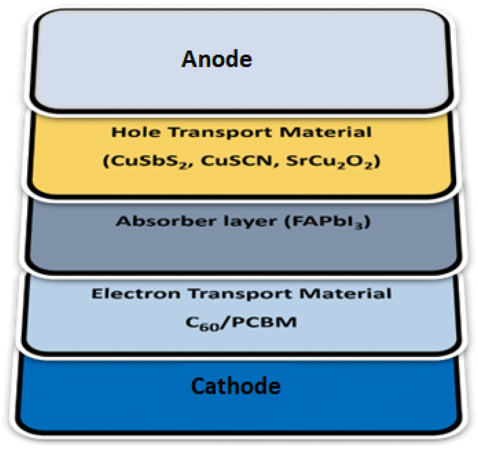
Solar cell capacitance simulator software SCAPS (ver.3.3.10) under AM1.5G (100 mW cm−2) solar spectrum with 300 K temperature has been used as a simulation tool to observe the electrical responses and impact on the perovskite structure. It is a one-dimensional opto-electrical simulator tool which can calculate the response of multi semiconductor layers. Its working principle is based on continuity and Poisson equations.27,28 Our simulated n–i–p structure composed of FTO/C60, PCBM/FAPbI3/CuSbS2, SrCu2O2 & CuSCN/Au, is shown in Fig. 1. To ensure efficient device performance, the thickness of the absorber layer, HTL, and ETL is tuned over a wide range to attain optimum values. FAPbI3 serves as the light absorber layer in all device configurations, sandwiched between the charge transport layers (ETL and HTL). The parameters required in the simulation such as thickness of each layer, e− and h+ mobility, bandgap of materials, effective density of states and defect density are precisely taken from different experimental and theoretical published work, see Table 1. The thermal velocity for e− and h+ are set to 1 × 107 cm s−1. The value of work function (front contact – FTO) and electrode (back contact – Au) are considered as 4.04 eV and 5.9 eV respectively.
 |
| | Fig. 1 Schematic visualization of device architecture. | |
Table 1 Input parameters for optoelectronic simulation
| Parameters |
SrCu2O2 (ref. 29) |
CuSbS2 (ref. 30) |
CuSCN31,32 |
FAPbI3 (ref. 4 and 33) |
C60 (ref. 34) |
PCBM35 |
| Thickness (nm) |
150 |
150 |
150 |
300 |
150 |
150 |
| Band gap (eV) |
3.3 |
1.58 |
3.2 |
1.51 |
1.7 |
2 |
| e− affinity (eV) |
2.2 |
4.2 |
1.9 |
4 |
3.9 |
4.2 |
| Permittivity |
9.77 |
14.6 |
10 |
6.6 |
4.2 |
3.9 |
| CB effective density of states (cm−3) |
2.2 × 10¹⁸ |
2.0 × 10¹⁸ |
2.2 × 10¹⁹ |
1.2 × 10¹⁹ |
8 × 10¹⁹ |
2.5 × 10²¹ |
| VB effective density of states (cm−3) |
1.8 × 10¹⁹ |
1.0 × 10¹⁹ |
1.8 × 10¹⁹ |
2.9 × 10¹⁸ |
8 × 10¹⁹ |
2.5 × 10²¹ |
| Mobility of e− |
0.1 |
49 |
2 × 10⁻⁴ |
2.7 |
8 × 10⁻² |
0.2 |
| Mobility of h+ |
0.46 |
49 |
1 × 10⁻² |
1.8 |
3.5 × 10⁻³ |
0.2 |
| Density of n-type doping |
0 |
0 |
0 |
1 × 10¹⁶ |
2.6 × 10¹⁷ |
2.9 × 10¹⁷ |
| Density of p-type doping |
3.6 × 10¹⁸ |
1 × 10¹⁸ |
1 × 10¹⁸ |
1 × 10¹⁶ |
0 |
0 |
| Density of defects |
1 × 10¹⁵ |
1 × 10¹⁵ |
1 × 10¹⁵ |
1 × 10¹⁴ |
1 × 10¹⁵ |
1 × 10¹⁵ |
| Interface defects |
1 × 10¹² |
1 × 10¹² |
1 × 10¹² |
|
1 × 10¹² |
1 × 10¹² |
3 Result and discussion
The primary focus of this research was to investigate the effect of different charge transport materials on the performance of FAPbI3 solar cell. In this regard, the energy band alignment, electric field, recombination and IV are first investigated for each structure. For optimized layers, the thickness of the absorber layer, ETL and HTL is varied initially. After identifying the optimized thickness, the doping concentration of absorber and charge transport layers are optimized. Influence of defect density was observed after getting optimized values of the configuration. Finally, the effect of temperature on the performance of device configuration is observed.
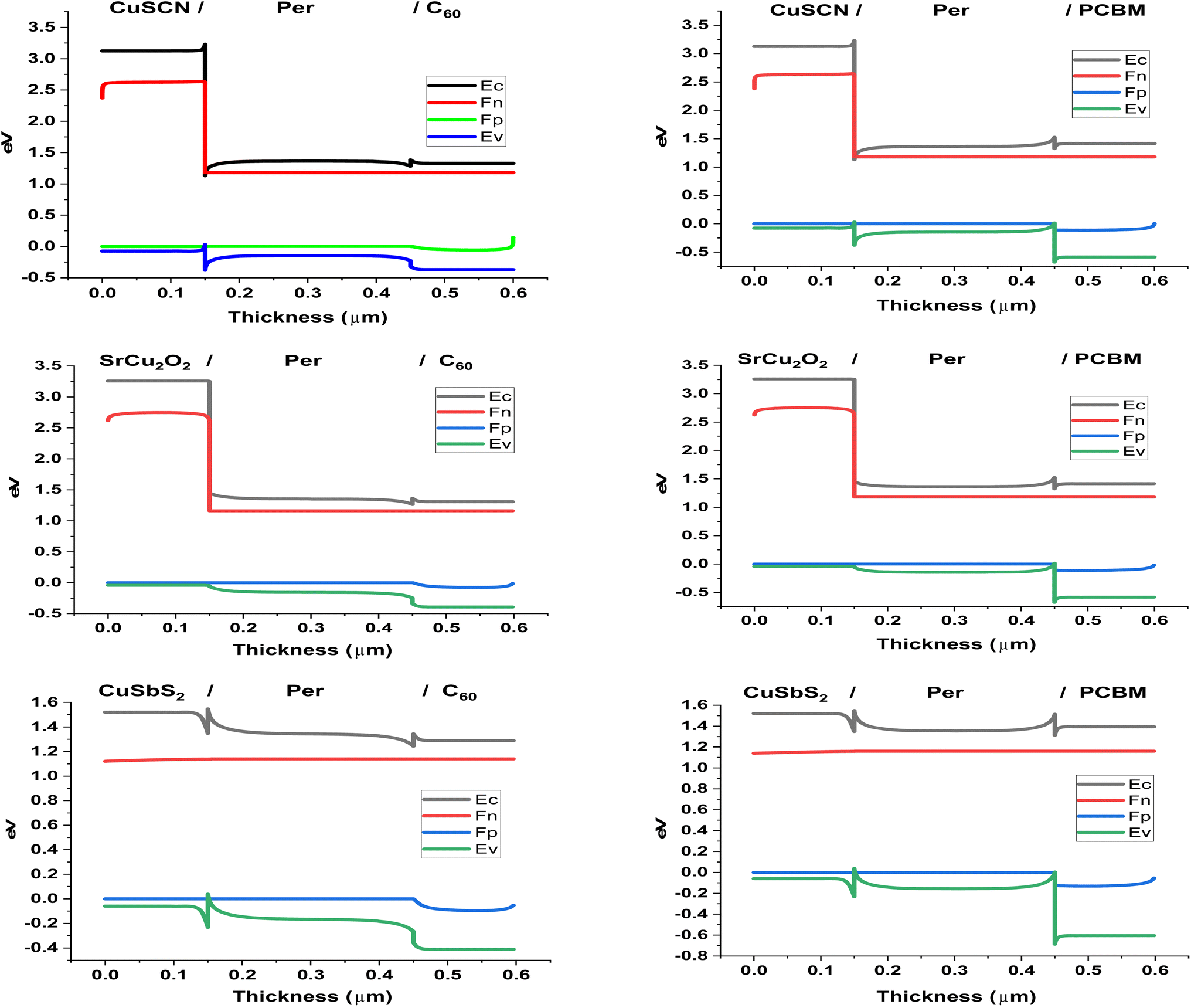
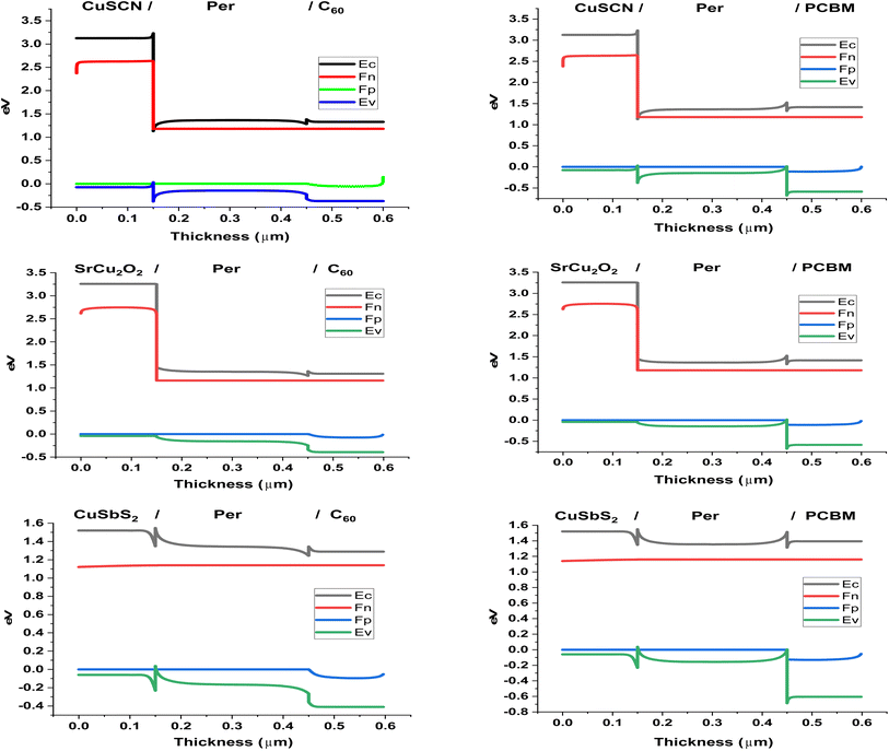
3.1 Energy band alignment
The energy band alignment of the charge transport material (HTL & ETL) with the perovskite material plays a very important role in the performance of the PSC. For efficient separation of electrons from the perovskite material the conduction band of ETL and PSC should align with minimum offset, while their valence band should have a large offset. If the valence bands are near then there is a probability that holes will flow to the ETL which would cause recombination. Similarly for separation of holes from the perovskite material the valence band of HTL and PSC should align, while their conduction band should have a large offset. If the conduction bands are near then there is a probability that electrons will flow to the HTL which would cause recombination.
Fig. 2 shows the energy band alignment of the different structures while Table 2 presents conduction band offset (CBO) and valence band offset (VBO) of the CTL with the perovskite material. SrCu2O2 makes perfect band alignment as its valence band has minimum offset of −0.01 eV with valence band of perovskite and large conduction band offset of 1.8 eV. The valence band of CuSbS2 forms a spike at the heterojunction of 0.27 eV which may increase the flow of holes but due to its small conduction band offset of −0.2 eV, electrons may also cross over, contributing in recombination. While the CuSCN forms a cliff of −0.41 at the interface which causes large hurdles for the holes to cross over, hence increasing recombination and reducing performance.
 |
| | Fig. 2 Energy band alignment of PSC layers. | |
Table 2 CBO and VBO at interfaces
| Interface |
CBO (eV) |
VBO (eV) |
| ETL/perovskite |
| C60/perovskite |
0.1 |
0.09 |
| PCBM/perovskite |
−0.2 |
0.69 |
![[thin space (1/6-em)]](https://www.rsc.org/images/entities/char_2009.gif) |
| Perovskite/HTL |
| Perovskite/SrCu2O2 |
1.8 |
−0.01 |
| Perovskite/CuSbS2 |
−0.2 |
0.27 |
| Perovskite/CuSCN |
2.1 |
−0.41 |
Similarly, for the ETL energy band alignment with the perovskite, both materials form small conduction band offsets. C60 forms a small spike of 0.1 eV while PCBM forms a small cliff of −0.2 eV. The PCBM outperforms the C60 due to the larger valence band offset of 0.69 eV it forms with the perovskite, which blocks the crossing over of the holes. Due to C60 small VBO of 0.09 eV, holes also flow to the ETL which causes increase in recombination.
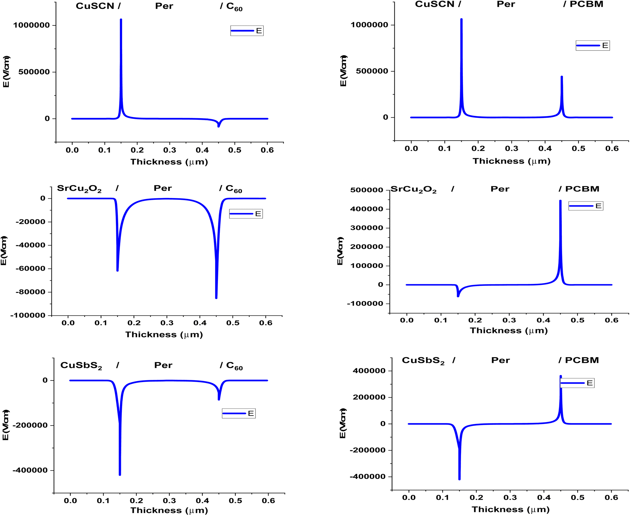
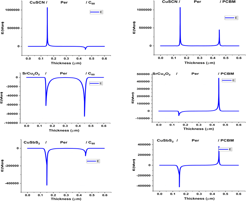
3.2 Electric field
The electric field produced by the charge transport material with the perovskite helps in separating the charge carriers in the perovskite. High electric field at the interface will separate more charge carriers as its influence will be deeper in the perovskite material. Fig. 3 shows the electric field produced by the CTM in the different PSC structures. A positive band offset (spike) increases the built in potential at the interface while a negative band offset (cliff) reduces the built in potential. It can be seen that in the ETL the C60 produces a negative electric field due to the positive conduction band offset (0.1 eV). While the PCBM produces a positive electric field due to the large negative conduction band offset (−0.2 eV). The negative conduction band offset not only reduces the built in potential but the cliff also blocks the flow of electrons to the ETL. The electrons accumulate at the heterojunction and produce its own electric field, opposite to the heterojunction's; thus, a positive electric field is obtained.
 |
| | Fig. 3 Electric field at PSC layer interfaces. | |
Similarly, for the HTL the CuSbS2 produces the negative electric field due to its large positive valence band offset (0.27 eV). The electric field by SrCu2O2 is also negative because the valence band offset is very minute (−0.01 eV). While CuSCN produced a positive electric field due to its large negative valence band offset (−0.41 eV) which blocks the flow of holes to the HTL.
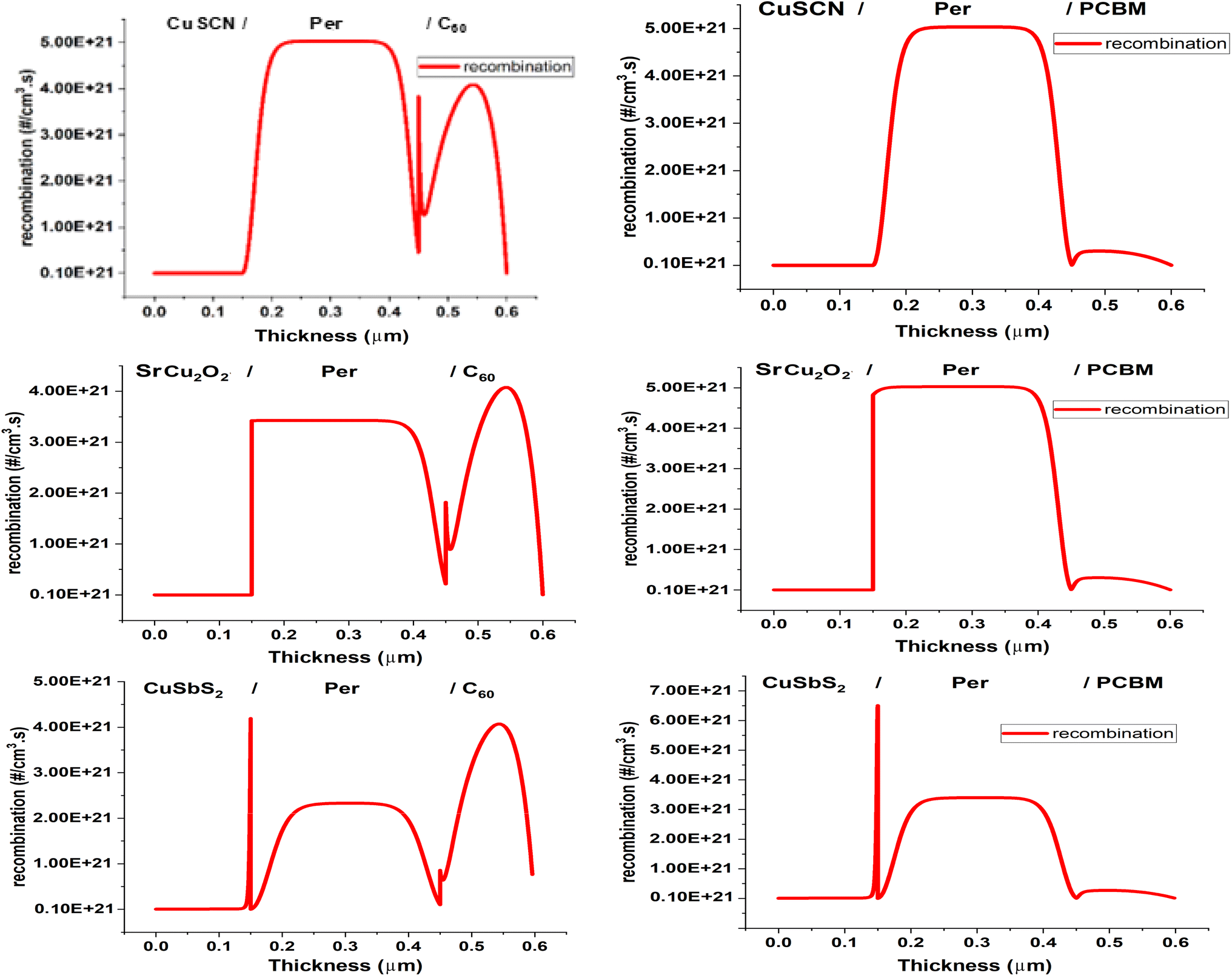
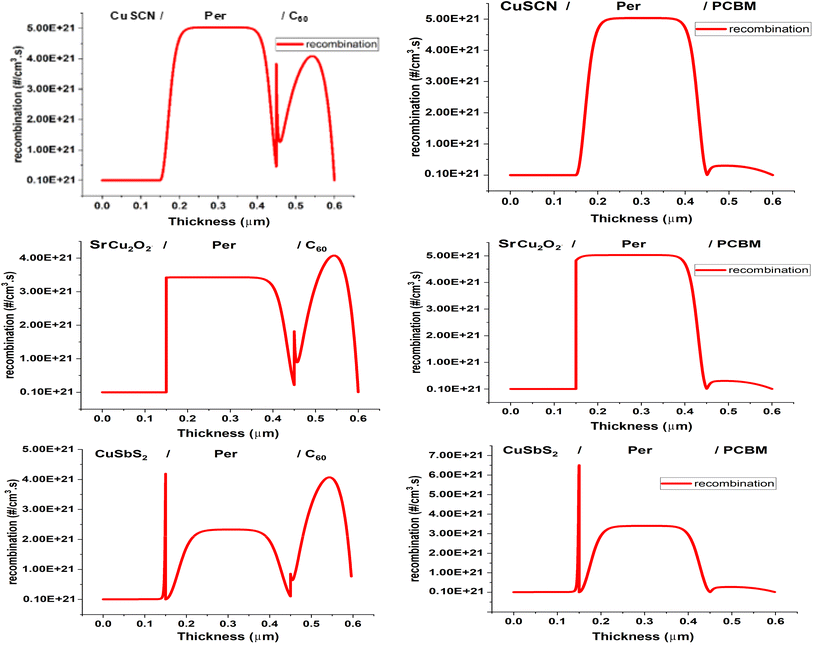
3.3 Recombination
Recombination is the recombining of the photogenerated charge carriers. Ideal PSC should have minimum recombination at the CTL/perovskite interface so that maximum carriers can be collected. Fig. 4 shows the recombination occurring in the PSC structures. The PCBM makes an acceptable CBO of −0.2 eV and large VBO with the perovskite material ensuring the smooth flow of electrons to the ETL where they are transported to the electrode for collection. The ETL cause minimum recombination at the heterojunction. As for C60, due to the low valence band offset, holes also flow from the perovskite to the ETL. This causes an increase in recombination in the ETL and reduces performance.
 |
| | Fig. 4 Recombination in PSC structures. | |
For the HTL SrCu2O2 forms the best energy band alignment with small VBO and large CBO. This ensures the smooth flow of the holes to the HTL while the electrons are blocked, causing minimum recombination at the heterojunction. The CuSbS2 forms small VBO and CBO which causes both holes and electrons to flow to the HTL. This causes an increase in recombination in it and reduces performance. While CuSCN forms a large VBO which blocks the flow of holes to the HTL and increases recombination.
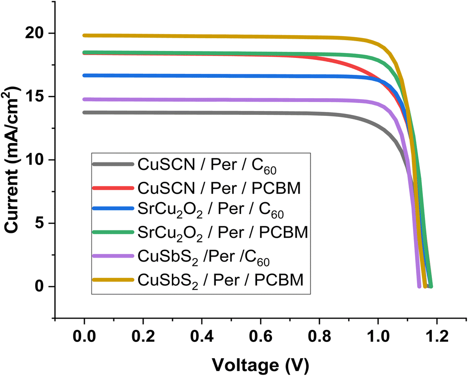
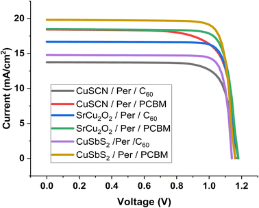
3.4 IV characteristics
Fig. 5 shows the IV characteristics of the six different structures. From the above-mentioned factors, it can be seen that the PCBM structures outperform the C60 structures. As less recombination occurs in PCBM, more current is produced. This leads to more efficiency and better performance.
 |
| | Fig. 5 IV of PSC structures. | |
3.5 Effect of absorber layer thickness and defect density
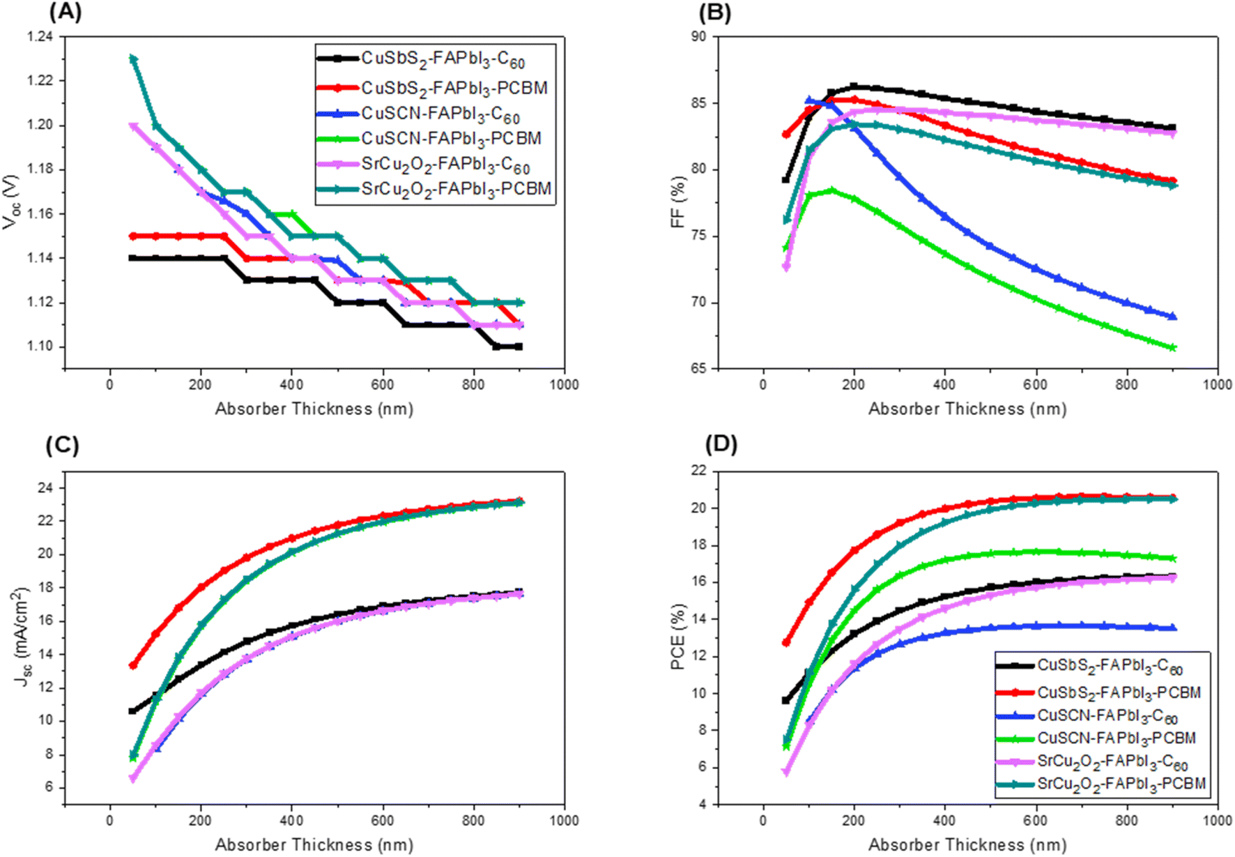
Absorber layer thickness is one of the major parameters in the configuration of solar cell. The thickness variation causes significant effect on the device output VOC, JSC, FF and PCE. In order to optimize the thickness of the absorber layer, it has been varied from 50 nm to 900 nm with an increment of 50 nm. Fig. 6 shows the effect of varying absorber thickness on device output characteristics. The detailed comparative analysis of device output characteristics with and without optimized absorber layer thickness is summarized in Table 3. It can be seen that as we start increasing the thickness of absorber layer from its initial value, the PCE increases. This is due to the fact that increase in absorber layer thickness provides more area for light to get absorbed which elevates the JSC and hence PCE increases. However, after certain increase in PCE further increase in absorber layer thickness may not result in the improvement of output power. If we increase the absorber layer thickness further, the PCE starts to decrease. This is caused due to increase number of traps and majority of the excess carriers are not reaching the electrodes.36
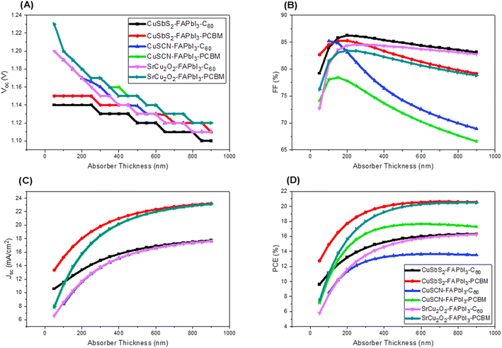 |
| | Fig. 6 Impact of varying absorber layer thickness on (A) Voc (B) FF (C) Jsc (D) PCE. | |
Table 3 Comparative analysis of device output characteristics for optimized & non-optimized absorber thickness
| Structure |
Status |
Absorber thickness (nm) |
VOC (V) |
JSC (mA cm−2) |
FF% |
PCE% |
| CuSbS2/C60 |
Initial |
300 |
1.13 |
14.78 |
85.91 |
14.47 |
| Optimized |
800 |
1.11 |
17.51 |
83.57 |
16.28 |
| CuSCN/C60 |
Initial |
300 |
1.16 |
13.74 |
79.42 |
12.67 |
| Optimized |
550 |
1.13 |
16.33 |
73.32 |
13.6 |
| SrCu2O2/C60 |
Initial |
300 |
1.15 |
13.77 |
84.52 |
13.49 |
| Optimized |
800 |
1.11 |
17.39 |
83.12 |
16.16 |
| CuSbS2/PCBM |
Initial |
300 |
1.14 |
19.82 |
84.46 |
19.22 |
| Optimized |
650 |
1.13 |
22.54 |
80.94 |
20.62 |
| CuSCN/PCBM |
Initial |
300 |
1.17 |
18.43 |
75.75 |
16.36 |
| Optimized |
550 |
1.14 |
21.64 |
71.03 |
17.63 |
| SrCu2O2/PCBM |
Initial |
300 |
1.17 |
18.49 |
83.06 |
17.98 |
| Optimized |
700 |
1.13 |
22.51 |
80.01 |
20.45 |
As far as the effect on VOC is concerned, the graph in Fig. 2(A) shows significant dip as absorber thickness is increased. As the absorber thickness increases, carrier concentration increases and hence resulting in higher photo-generated current. However, due to high recombination rate and higher dark current VOC significantly decreased.
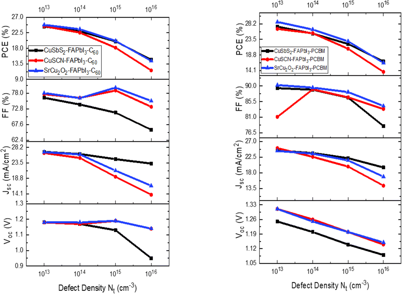
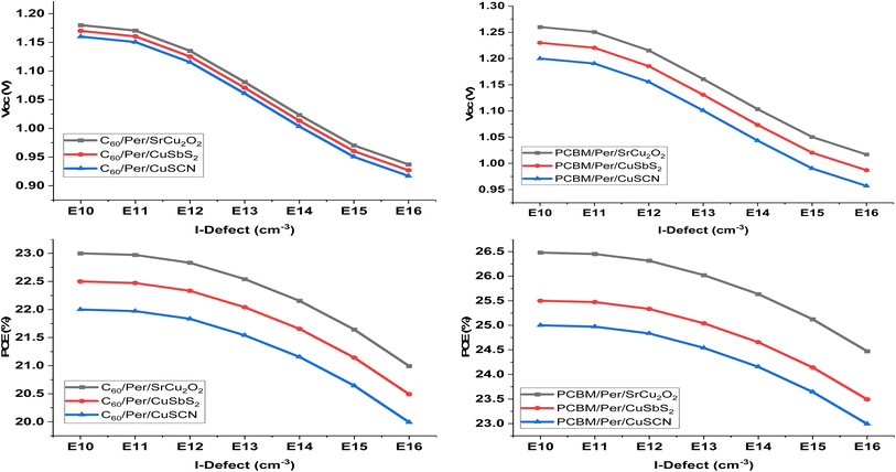
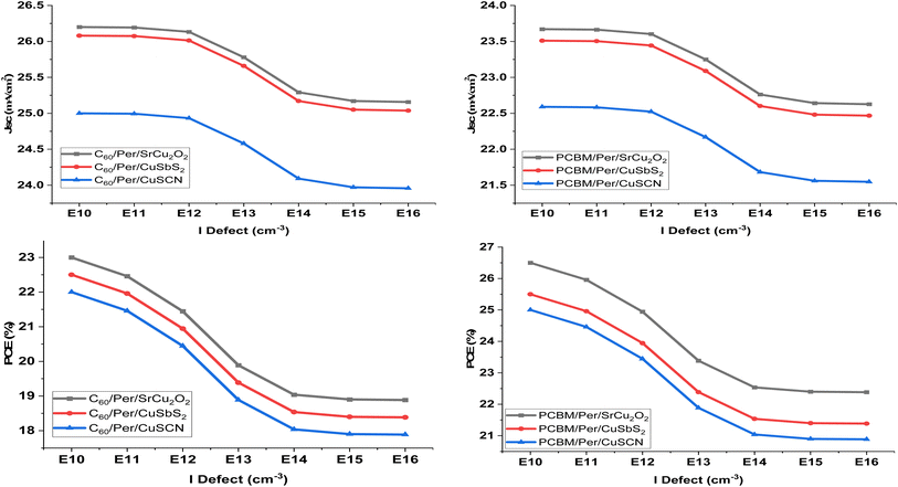
The absorber defect density (Nt) has a significant effect on the performance of the solar cell and the optimized thickness as it traps the photo-generated carriers inside the trap levels. This reduces the carrier life time which in turn reduces the absorption length and increases the recombination.38,39 In order to investigate the effect of absorber Nt, the energetic distribution of the defects is kept as Gaussian distribution. The literature on different experimental findings showed better output performance for perovskite of highly crystalline nature at lower Nt. From the results in Fig. 7 it can be seen that at lower Nt (1 × 10¹¹ and 1 × 10¹²), there is a negligible effect on the performance of the solar cell. However, when it increased from 1 × 10¹³ to 1 × 10¹⁶, significant reduction in JSC and PCE is observed. In order to achieve an optimum and more practical results, Nt is chosen at 1 × 10¹⁴ throughout this work.40
 |
| | Fig. 7 Influence of defect density (Nt) on device output characteristics. | |
Table 4 depicts the optimized thickness and output parameters on different defect densities for the proposed device structures.
Table 4 Optimized solar cell parameters for different Nt of proposed structures
| Nt |
Thickness (nm) |
Doping concentration |
VOC (V) |
JSC (mA cm−2) |
FF (%) |
PCE (%) |
| 1 × 10¹³ |
900 |
1 × 10¹⁸ |
1.31 |
24.29 |
90.24 |
28.78 |
| 1 × 10¹⁴ |
700 |
1 × 10¹⁸ |
1.25 |
23.51 |
89.5 |
26.48 |
| 1 × 10¹⁵ |
550 |
1 × 10¹⁸ |
1.2 |
21.56 |
88.23 |
22.93 |
| 1 × 10¹⁶ |
400 |
1 × 10¹⁸ |
1.15 |
16.89 |
84.22 |
16.41 |
| 1 × 10¹⁷ |
300 |
1 × 10¹⁸ |
1.18 |
10.9 |
76.15 |
9.88 |
| 1 × 10¹⁸ |
100 |
1 × 10¹⁸ |
1.0 |
7.65 |
60.37 |
4.65 |
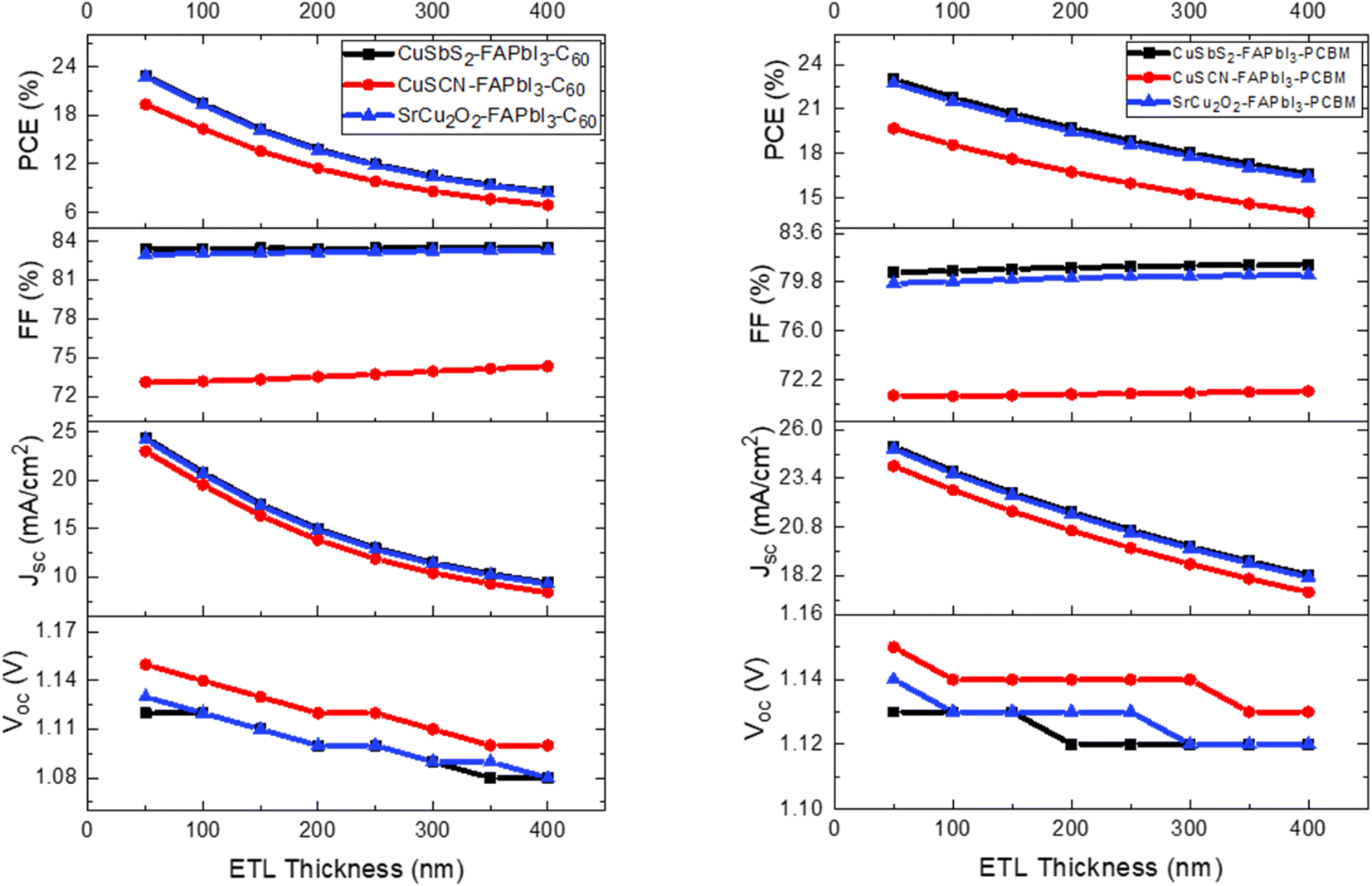
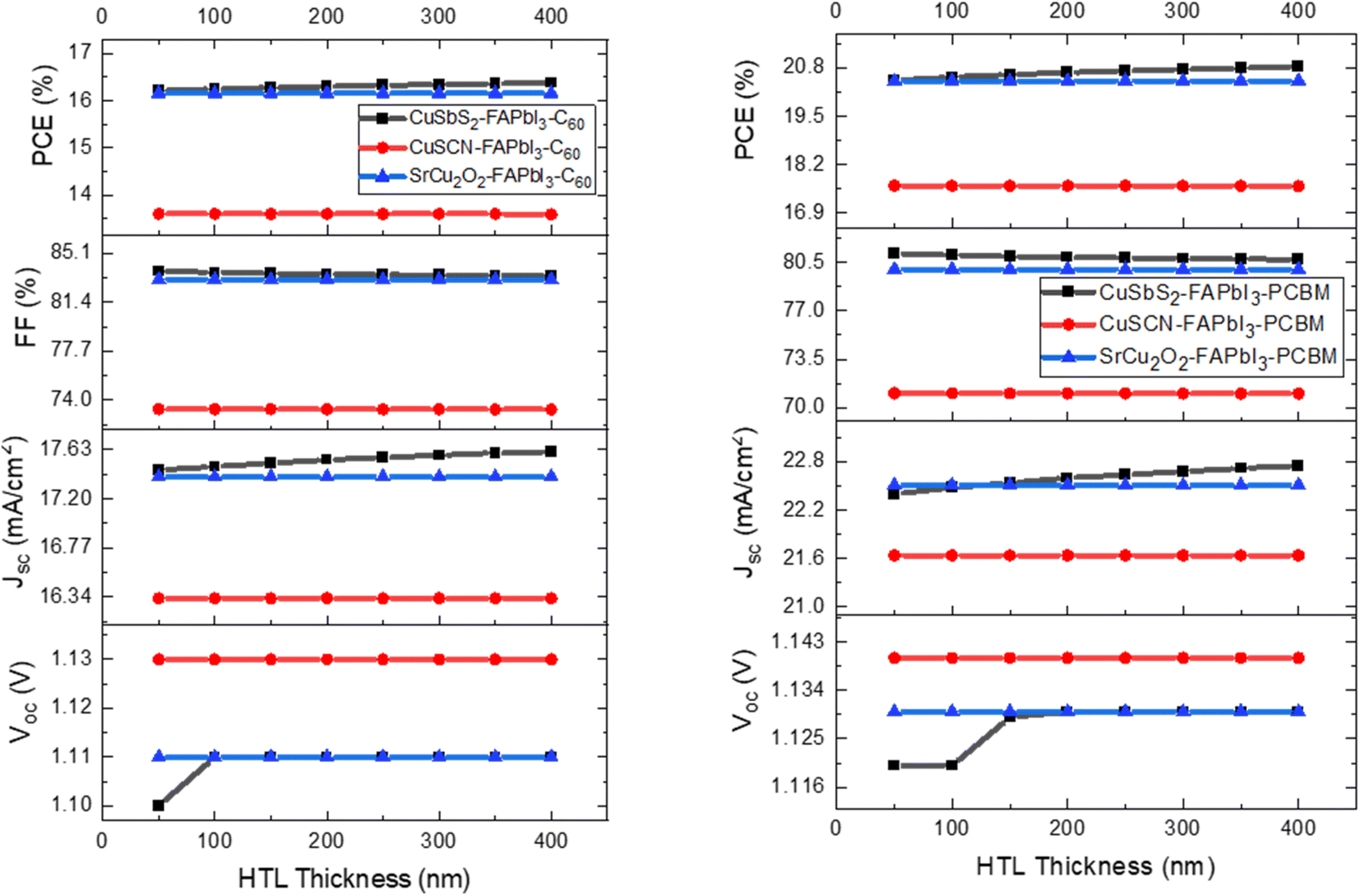
3.6 Effect of CTL thickness
The variation in CTL thickness for proposed device structures has been analyzed in detail by observing their effect on the device output characteristics. The CTL thickness is varied from 50 nm to 400 nm with an increment of 50 nm. Fig. 8 shows the effect of varying ETL thickness and Fig. 9 shows the effect of varying HTL thickness on the device output characteristics. The increase in CTL thickness leads to increase in series resistance which makes it difficult for the charge ions to reach the electrodes and hence recombination occurs. Besides transporting the photo generated charge carriers, the other function of the CTL is to act as a buffer layer between the organic perovskite layer and metal electrodes as direct contact between the two layers produce high series resistance. Too thin CTL are not able to provide adequate separation between the two layers. Therefore, in this study, the optimum thickness for ETL and HTL are chosen at 100 nm as further increase leads to reduction in PCE.
 |
| | Fig. 8 Influence of ETL thickness on device output characteristics. | |
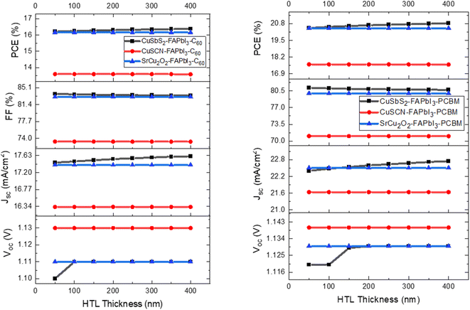 |
| | Fig. 9 Influence of HTL thickness on device output characteristics. | |
3.7 Effect of absorber doping concentration
The output performance of the perovskite solar cells is highly influenced by the quality and structure of the absorber layer. Doping concentration and defect density plays a significant role in obtaining effective device outcomes. To investigate the effect of doping concentration on the output performance of the solar cell, the acceptor doping concentration of the absorber layer is varied from 1 × 10¹² to 1 × 1020 cm−3. The optimized thickness and doping concentration in the remaining layers are kept constant. It is quite evident from the Fig. 10 that the doping concentration from 1 × 10¹² to 1 × 1015 cm−3 has a very minute effect on the output performance of the cell. However, from 1 × 1016 cm−3 and onwards the VOC and PCE increased significantly due to the decrease in reverse saturation current and increase in charge carrier concentration. An increased efficiency of up to 4% can be seen for each structure with an increase of doping concentration. A decrease in JSC and PCE can be observed in CuSbS2 structures after doping concentration increased to 1 × 1017 cm−3. Heavy doping leads to increased recombination because of too many scattering centers.37 Furthermore, it causes the perovskite to change from semiconductor to metallic nature, which has a significant effect on the charge carrier transport mechanism. From the results it can be concluded that apart from CuSbS2 the optimized doping concentration for all the proposed structures is achieved at 1 × 1018 cm−3.
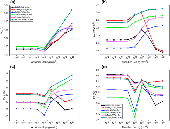 |
| | Fig. 10 Influence of absorber doping concentration on device output characteristics (a) Voc (b) Jsc (c) PCE (d) FF. | |
3.8 Effect of CTL doping
To investigate the doping effect of CTL on the performance of perovskite solar cell, the doping levels are varied from 1 × 10¹² to 1 × 1020 cm−3. The acceptor concentration (NA) is increased for HTM while donor concentration (ND) is increased for ETM. The results are analyzed to find the optimized parameters for proposed structures. The results in Fig. 11 shows that by increasing NA from 1 × 1016 cm−3 to 1 × 1018 cm−3, a significant increase in PCE is observed for CuSbS2 and CuSCN. While in case of SrCu2O2, it is comparatively less. However, after 1 × 1018 cm−3 the saturation point is achieved. In this work we choose 1 × 1020 cm−3 value of doping for CuSbS2 and CuSCN to attain efficient results.
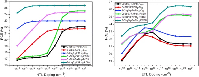 |
| | Fig. 11 Influence of CTL doping on power conversion efficiency of the device. | |
The behavior of the perovskite solar cell is different for both C60 and PCBM as evident from Fig. 11. The structures with C60 displayed better PCE as compared to PCBM when the doping concentration is increased up to 1 × 1015 cm−3. The structures with PCBM showed a steady increase in PCE initially when the doping concentration is increased till 1 × 1015 cm−3. However, further increased in doping concentration showed significant rise in PCE. Finally, saturation occurred after 1 × 1019 cm−3 due to the Moss–Burstein effect.41
The optimized doping for the proposed structures with C60 is found at 1 × 1015 cm−3 while, for PCBM it is found at 1 × 1019 cm−3. These doping levels give maximum PCE of 23.53% and 26.48% respectively. Table 5 depicts the solar cell parameters with possible combination of HTM and ETM. The maximum PCE of 26.48% is achieved for FTO/PCBM/FAPbI3/SrCu2O2/Au.
Table 5 Optimized solar cell parameters along with device output characteristics for proposed structures
| HTM |
ETM |
Optimized doping of HTM (cm−3) |
Optimized doping of ETM (cm−3) |
VOC (V) |
JSC (mA cm−2) |
FF (%) |
PCE (%) |
| CuSbS2 |
PCBM |
1020 |
1019 |
1.2 |
23.67 |
88.91 |
25.27 |
| C60 |
1020 |
1016 |
1.17 |
26.20 |
74.25 |
22.94 |
| CuSCN |
PCBM |
1019 |
1019 |
1.26 |
22.59 |
89.01 |
25.37 |
| C60 |
1020 |
1015 |
1.17 |
25.00 |
76.46 |
22.55 |
| SrCu2O2 |
PCBM |
1018 |
1019 |
1.25 |
23.51 |
89.5 |
26.48 |
| C60 |
1018 |
1015 |
1.18 |
26.08 |
76.38 |
23.53 |
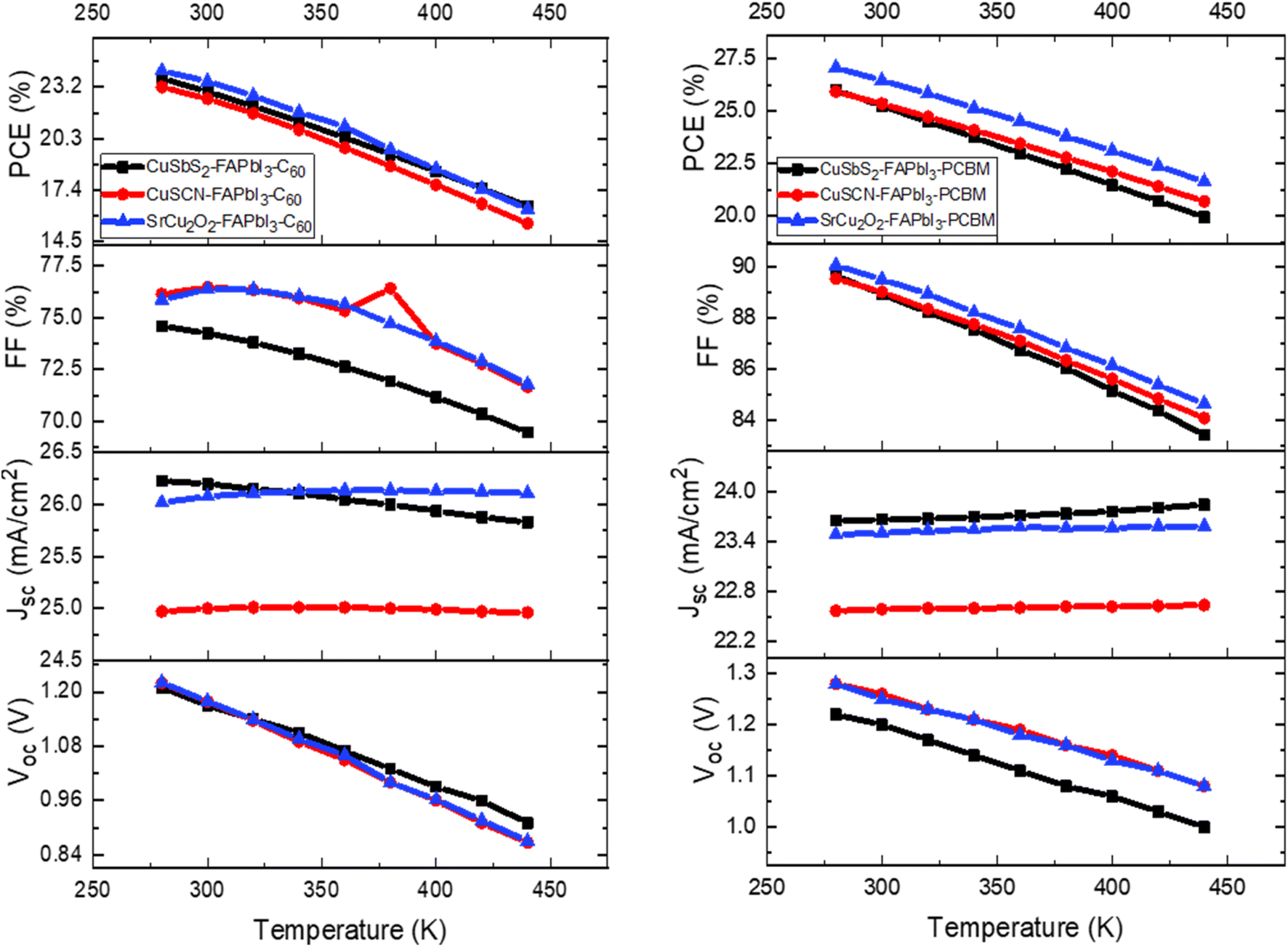
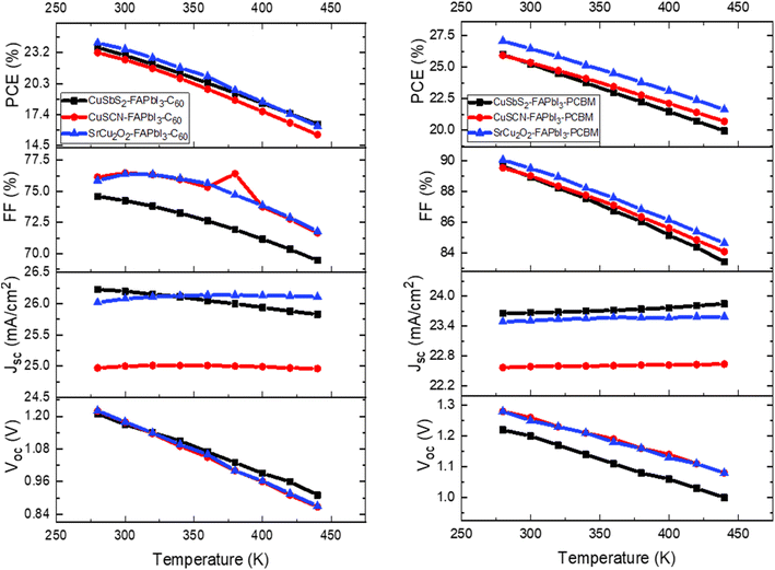
3.9 Effect of temperature on solar cell performance
To investigate the effect of working temperature on the solar cell performance, the temperature is varied from 280 to 400 K for all the proposed structures. All other parameters including absorber thickness, doping concentration and CTL thickness are set to their optimized values given in Table 3. From the results of Fig. 12 it is observed that as working temperature is increased the output performance of the structures reduced drastically. This occurs because series resistance (RS) increases with the rise in temperature which incites reduction in diffusion length and ultimately leads to increase in recombination rate. This trend is consistent with prior research on temperature-dependent solar cell performance.42 The recommended temperature of the simulated model is fixed at 300 K to attain improved cell efficiency.
 |
| | Fig. 12 Influence of working temperature on device output characteristics. | |
3.10 Effect of interface defects
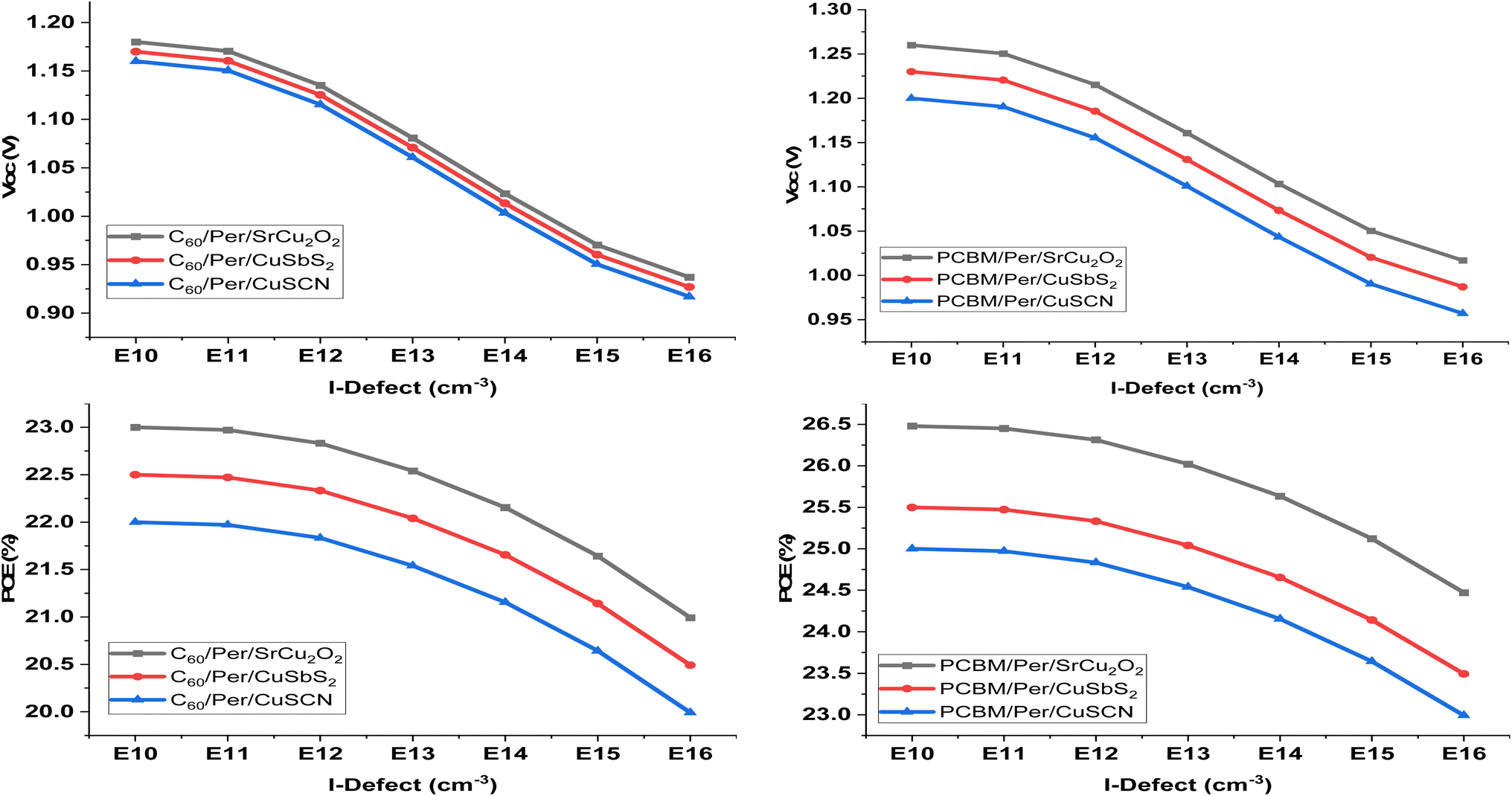
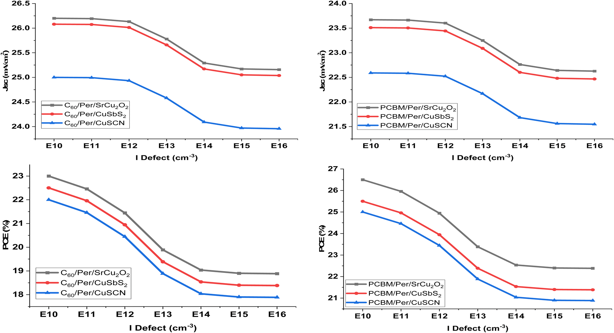
The perovskite solar cell has two main interfaces. The first is the ETL/perovskite interface while the second is the HTL/perovskite interface. The defects at the interface occur due to the dangling bonds and grain boundaries formed at the surfaces of the materials. These act as traps for the charge carriers and capture them when they are being transported to the CTL from the perovskite material. To study the effect of interface defects on the PSC performance, both interface defects are changed from 1 × 10¹⁰ to 1 × 1016 cm−3. Fig. 13 show the effect of HTL/perovskite interface defect on PSC performance while Fig. 14 show the effect of perovskite/ETL interface defects.
 |
| | Fig. 13 Influence of HTL/perovskite defects on device output characteristics. | |
 |
| | Fig. 14 Influence of ETL/perovskite defects on device output characteristics. | |
The HTL/perovskite interface reduces the VOC of all the structures as the defect are increased. This happens because due to the increasing number of interface defects more traps are produced which capture more and more holes. While the ETL/perovskite interface reduces the JSC of the PSC as the defect are increased because a greater number of electrons are captured in the traps. Both the interface defects reduce the performance of the PSC.
4 Conclusion
In this work, formamidinium lead tri-iodide (FAPbI3) is investigated with three copper based HTLs (SrCu2O2, CuSCN, CuSbS2) and two carbon based ETLs (C60 and PCBM) using SCAPS 1-D simulation software. Each CTL is observed separately by using possible combination with FAPbI3 absorber layer to identify optimum values for each layer. Optimum thickness and doping concentration for all the layers of the different structures are found by adopting a systematic study. It was concluded from the study that by using optimized values for each structure the best cell output performance is observed. Moreover, it is also observed that increase in doping density of ETL and HTL boots up the cell performance. Among all the structures, SrCu2O2/FAPbI3/PCBM showed the most efficient and promising results having PCE of 26.48% with 23.52 mA cm−2 JSC, 1.25 V VOC and 89.5% FF. The optimized thickness is observed at 750 nm, 150 nm and 100 nm for the absorber layer, HTL and ETL respectively. While the optimized doping concentration is observed at 1 × 10¹⁸ and 1 × 10¹⁹ for the absorber and CTLs respectively.
Data availability
The datasets generated and analyzed during the current study are available from the corresponding author on reasonable request.
Conflicts of interest
There are no conflicts to declare.
Acknowledgements
This research did not receive any specific grant from funding agencies in the public, commercial, or not-for-profit sectors. We are very thankful to Marc Burgelman, department of electronics and information systems at the University of Gent, Belgium, for providing SCAPS simulation software.
References
- J.-P. Correa-Baena, et al., The rapid evolution of highly efficient perovskite solar cells, Energy Environ. Sci., 2017, 10(3), 710–727 RSC.
- S. Bhattarai and T. Das, Optimization of the perovskite solar cell design to achieve a highly improved efficiency, Opt. Mater., 2021, 111, 110661 CrossRef CAS.
- R. C. Shallcross, Y. Zheng, S. S. Saavedra and N. R. Armstrong, Determining band-edge energies and morphology-dependent stability of formamidinium lead perovskite films using spectroelectrochemistry and photoelectron spectroscopy, J. Am. Chem. Soc., 2017, 139(13), 4866–4878 CrossRef CAS PubMed.
- K. Galkowski, et al., Determination of the exciton binding energy and effective masses for methylammonium and formamidinium lead tri-halide perovskite semiconductors, Energy Environ. Sci., 2016, 9(3), 962–970 RSC.
- U. Syafiq, N. Ataollahi and P. Scardi, Progress in CZTS as hole transport layer in perovskite solar cell, Sol. Energy, 2020, 196, 399–408 CrossRef CAS.
- S. Abdelaziz, A. Zekry, A. Shaker and M. Abouelatta, Investigating the performance of formamidinium tin-based perovskite solar cell by SCAPS device simulation, Opt. Mater., 2020, 101, 109738 CrossRef CAS.
- F. Baig, Y. H. Khattak, A. Shuja, K. Riaz and B. M. Soucase, Performance investigation of Sb2Se3 based solar cell by device optimization, band offset engineering and Hole Transport Layer in SCAPS-1D, Curr. Appl. Phys., 2020, 20(8), 973–981 CrossRef.
- A. Kojima, K. Teshima, Y. Shirai and T. Miyasaka, Organometal halide perovskites as visible-light sensitizers for photovoltaic cells, J. Am. Chem. Soc., 2009, 131(17), 6050–6051 CrossRef CAS PubMed.
- S. S. Hussain, S. Riaz, G. A. Nowsherwan, K. Jahangir, A. Raza, M. J. Iqbal, I. Sadiq, S. M. Hussain and S. Naseem, Numerical Modeling and Optimization of Lead-Free Hybrid Double Perovskite Solar Cell by Using SCAPS-1D, J. Renewable Energy, 2021, 2021, 12 Search PubMed.
- F. Aslan, H. Esen and F. Yakuphanoglu, Al/P-Si/Coumarin: TiO2/Al organic-inorganic hybrid photodiodes: investigation of electrical and structural properties, Silicon, 2020, 12(9), 2149–2164 CrossRef.
- W. S. Yang, et al., Iodide management in formamidinium-lead-halide–based perovskite layers for efficient solar cells, Science, 2017, 356(6345), 1376–1379 CrossRef CAS PubMed.
- N. Anttu, Shockley–Queisser detailed balance efficiency limit for nanowire solar cells, ACS Photonics, 2015, 2(3), 446–453 CrossRef CAS.
- S. A. Moyez and S. Roy, Dual-step thermal engineering technique: a new approach for fabrication of efficient CH3NH3PbI3-based perovskite solar cell in open air condition, Sol. Energy Mater. Sol. Cells, 2018, 185, 145–152 CrossRef CAS.
- M. Jamal, et al., Effect of defect density and energy level mismatch on the performance of perovskite solar cells by numerical simulation, Optik, 2019, 182, 1204–1210 CrossRef CAS.
- S. Rai, B. Pandey and D. Dwivedi, Modeling of highly efficient and low cost CH3NH3Pb (I1-xClx) 3 based perovskite solar cell by numerical simulation, Opt. Mater., 2020, 100, 109631 CrossRef CAS.
- A. K. Jena, A. Kulkarni and T. Miyasaka, Halide perovskite photovoltaics: background, status, and future prospects, Chem. Rev., 2019, 119(5), 3036–3103 CrossRef CAS PubMed.
- M. B. Kanoun, A.-A. Kanoun, A. E. Merad and S. Goumri-Said, Device design optimization with interface engineering for highly efficient mixed cations and halides perovskite solar cells, Results Phys., 2021, 20, 103707 CrossRef.
- R. Pandey and R. Chaujar, Technology computer aided design of 29.5% efficient perovskite/interdigitated back contact silicon heterojunction mechanically stacked tandem solar cell for energy-efficient applications, J. Photonics Energy, 2017, 7(2), 022503 CrossRef.
- Q. Han, et al., Single crystal formamidinium lead iodide (FAPbI3): insight into the structural, optical, and electrical properties, Adv. Mater., 2016, 28(11), 2253–2258 CrossRef CAS PubMed.
- S. Wozny, et al., Controlled humidity study on the formation of higher efficiency formamidinium lead triiodide-based solar cells, Chem. Mater., 2015, 27(13), 4814–4820 CrossRef CAS.
- G. E. Eperon, S. D. Stranks, C. Menelaou, M. B. Johnston, L. M. Herz and H. J. Snaith, Supplementary information Formamidinium of Formamidinium lead trihalide: a broadly tunable perovskite for efficient planar heterojunction solar cells, Energy Environ. Sci., 2014, 7(3), 982 RSC.
- D. Wang, M. Wright, N. K. Elumalai and A. Uddin, Stability of perovskite solar cells, Sol. Energy Mater. Sol. Cells, 2016, 147, 255–275 CrossRef CAS.
- S. Z. Haider, H. Anwar and M. Wang, A comprehensive device modelling of perovskite solar cell with inorganic copper iodide as hole transport material, Semicond. Sci. Technol., 2018, 33(3), 035001 CrossRef.
- R. S. Sanchez and E. Mas-Marza, Light-induced effects on Spiro-OMeTAD films and hybrid lead halide perovskite solar cells, Sol. Energy Mater. Sol. Cells, 2016, 158, 189–194 CrossRef CAS.
- X. Zhao and N.-G. Park, Stability issues on perovskite solar cells, Photonics, 2015, 2(4), 1139–1151 CrossRef CAS.
- Y. Zhang, et al., Flexible, hole transporting layer-free and stable CH3NH3PbI3/PC61BM planar heterojunction perovskite solar cells, Org. Electron., 2016, 30, 281–288 CrossRef CAS.
- W. Abdelaziz, A. Shaker, M. Abouelatta and A. Zekry, Possible efficiency boosting of non-fullerene acceptor solar cell using device simulation, Opt. Mater., 2019, 91, 239–245 CrossRef CAS.
- T. Minemoto and M. Murata, Impact of work function of back contact of perovskite solar cells without hole transport material analyzed by device simulation, Curr. Appl. Phys., 2014, 14(11), 1428–1433 CrossRef.
- M. Shasti and A. Mortezaali, Numerical Study of Cu2O, SrCu2O2, and CuAlO2 as Hole-Transport Materials for Application in Perovskite Solar Cells, Phys. Status Solidi A, 2019, 216(18), 1900337 CrossRef.
- C. Devi and R. Mehra, Device simulation of lead-free MASnI 3 solar cell with CuSbS 2 (copper antimony sulfide), J. Mater. Sci., 2019, 54(7), 5615–5624 CrossRef CAS.
- F. Azri, A. Meftah, N. Sengouga and A. Meftah, Electron and hole transport layers optimization by numerical simulation of a perovskite solar cell, Sol. Energy, 2019, 181, 372–378 CrossRef CAS.
- K. Chakraborty, M. G. Choudhury and S. Paul, Numerical study of Cs2TiX6 (X= Br−, I−, F− and Cl−) based perovskite solar cell using SCAPS-1D device simulation, Sol. Energy, 2019, 194, 886–892 CrossRef CAS.
- K. B. Nine, M. N. H. Shazon and S. A. Mahmood, Performance evaluation and comparative analysis of a highly efficient FAPbI 3-based perovskite solar cell, J. Opt. Soc. Am. B, 2020, 37(10), 2996–3004 CrossRef CAS.
- K. D. Jayan and V. Sebastian, Comprehensive device modelling and performance analysis of MASnI3 based perovskite solar cells with diverse ETM, HTM and back metal contacts, Sol. Energy, 2021, 217, 40–48 CrossRef.
- M. Shamna, K. Nithya and K. Sudheer, Simulation and optimization of CH3NH3SnI3 based inverted perovskite solar cell with NiO as Hole transport material, Mater. Today: Proc., 2020, 33, 1246–1251 CAS.
- T. M. Koh, et al., Formamidinium tin-based perovskite with low E g for photovoltaic applications, J. Mater. Chem. A, 2015, 3(29), 14996–15000 RSC.
- W. Liao, et al., Lead-free inverted planar formamidinium tin triiodide perovskite solar cells achieving power conversion efficiencies up to 6.22, Adv. Mater., 2016, 28(42), 9333–9340 CrossRef CAS PubMed.
- K. Sobayel, et al., A comprehensive defect study of tungsten disulfide (WS2) as electron transport layer in perovskite solar cells by numerical simulation, Results Phys., 2019, 12, 1097–1103 CrossRef.
- A. Zekry, A. Shaker, and M. Salem, Solar cells and arrays: principles, analysis, and design, in Advances in renewable energies and power technologies, Elsevier, 2018, pp. 3–56 Search PubMed.
- L. Lin, L. Jiang, Y. Qiu and Y. Yu, Modeling and analysis of HTM-free perovskite solar cells based on ZnO electron transport layer, Superlattices Microstruct., 2017, 104, 167–177 CrossRef CAS.
- V. Trukhanov, V. Bruevich and D. Y. Paraschuk, Effect of doping on performance of organic solar cells, Phys. Rev. B, 2011, 84(20), 205318 CrossRef.
- A. Sunny, S. Rahman, M. M. Khatun and S. R. A. Ahmed, Numerical study of high performance HTL-free CH3NH3SnI3-based perovskite solar cell by SCAPS-1D, AIP Adv., 2021, 11(6), 065102 CrossRef CAS.
|
| This journal is © The Royal Society of Chemistry 2023 |
Click here to see how this site uses Cookies. View our privacy policy here. 
 Open Access Article
 This Open Access Article is licensed under a
  *a,
Muhammad Shahzaibb,
Shayan Tariq Jan
*a,
Muhammad Shahzaibb,
Shayan Tariq Jan