
 Open Access Article
 This Open Access Article is licensed under a Creative Commons Attribution-Non Commercial 3.0 Unported Licence
Synthesis of WO3@WS2 core–shell nanostructures via solution-based sulfurization for improved performance of water splitting
Jianming Laiab,
Bingjie Wanga,
Yuedong Gonga,
Chenwei Suna,
Weilin Wangc and
Weiguang Yang *abd
*abd
aDepartment of Electronic Information Materials, School of Materials Science and Engineering, Shanghai University, Shanghai 200444, China
bZhejiang Institute of Advanced Materials, SHU, Jiashan, 314113, China
cHenan Power Battery Innovation Center Co., Ltd, No. 416, Muye Avenue, Xinxiang, 453004, China
dCollaborative Innovation Center of Henan Province for Motive Power and Key Materials, College of Chemistry and Chemical Engineering, Henan Normal University, Xinxiang, 453007, China
First published on 31st January 2023
Abstract
High light absorption capacity and excellent charge transportation are significant for superior water-splitting performance. Here, WO3/WS2 core–shell nanowire arrays were fabricated using a two-step hydrothermal method. The crystal phase, morphology, crystal structure, chemical composition, and optical properties were characterized using XRD, SEM, TEM, XPS, and UV-vis spectroscopy. Consequently, the photocurrent density of the as-prepared WO3/WS2 photoanode was 0.91 mA cm−2 (at 1.23 V vs. RHE), which showed a 112% increase compared to that with pristine WO3. The enhanced photoelectrochemical performance, we believe, was due to the promoted light response and improved separation as well as transportation at the WO3/WS2 interface.
1. Introduction
Compared with other hydrogen production techniques, photoelectrochemical (PEC) water splitting, which can directly convert solar energy into hydrogen, has emerged as a promising method to generate hydrogen due to its many advantages including sustainability and no pollutants.1–4 In 1972, using TiO2 as a photoanode in PEC water splitting was first reported by Fujishima and Honda.5 Since then, a huge amount of semiconductors have been tried as photoelectrodes, particularly many metal oxides.6–8Among various materials, tungsten trioxide (WO3), with a band gap at around 2.8 eV, has intrigued a lot of interest due to the following advantages: non-toxicity, high resistance to photocorrosion, a moderate hole diffusion length (∼150 nm), superior electron mobility (∼12 cm2 V−1 s−1) and a suitable valence band position for water oxidation.9–12 However, the PEC performance of WO3 is still not efficient enough due to two important problems: the recombination of photogenerated electron and hole pairs in the bulk, as well as a relative large band gap value.13,14 Thus, coupling with a narrow band gap semiconductor to form a heterostructure, seems to be an effective strategy to boost the PEC performance of WO3. For instance, Zheng reported a Z-scheme WO3/Cu2O heterojunction for enhanced PEC performance without external bias.15 Many other heterostructures, including WO3/Co3O4, WO3/BiVO4, WO3/g-C3N4, WO3/Ag2S, and WO3/Sb2S3 have also exhibited excellent PEC performance, which is due to more charge separation and transportation at the interface.13,16–21 Nevertheless, most of these studies have to consider the problem of lattice matching at the interface, which might induce some defects.
In particular, WO3/WS2 Z-scheme heterostructures have recently attracted considerable attention because of their unique structure. WS2 is an indirect band gap semiconductor with a good PEC activity,22 which matches well with WO3.23 Seo et al. reported an approach for synthesizing WO3/WS2 core–shell structures utilizing the WO3·0.33H2O phase using H2S gas for sulfurization.24 Lee et al. synthesized edge-exposed 1T phase WS2 on WO3 nanohelixes arrays by pre-annealing and CVD.25
Our approach was to create a sulfurized shell by a simple hydrothermal sulfurization process, which is more facile than others. Depending on this method, a WS2 shell was successfully synthesized at the surface of WO3 with intimate contact.
In this work, vertically-aligned one-dimensional (1-D) WO3 nanowire arrays were synthesized on the FTO substrate using the hydrothermal method. Then, after a simple sulfurization process, a narrow band gap WS2 was coated on the surface of WO3. The obtained photocurrent density of WO3/WS2 core–shell nanowire arrays increased by 112% compared to that of pristine WO3 nanowires. The enhanced PEC performance was illustrated through the investigation of crystal structure, morphology characterization, and optical properties. Furthermore, the application of a simple sulfurization process was helpful for the construction of visible-light active photoanode with high stability under illumination.
2. Experimental section
2.1 The growth of WO3 nanowire arrays
WO3 nanowire arrays were synthesized on an FTO substrate using the hydrothermal method. First of all, a dense layer was spin-coated on a cleaned FTO substrate followed by annealing at 500 °C using a solution containing 10 mL, 0.7 g titanium tetraisopropanolate (TTIP), and 12 μL of 36% HCL. Separately, 8.3 g of Na2WO4·2H2O was dissolved in 25 mL deionized water (DIW) and then a mixed acid solution (the mole ratio of HCl and H2SO4 was 5![[thin space (1/6-em)]](https://www.rsc.org/images/entities/char_2009.gif) :1) was slowly added until the pH value of the solution was approximately 3.2–3.5. Then, the pH value of this solution was adjusted to 4.2 using DIW. Forth, 1.0 g oxalic acid was added to adjust the pH value to about 1.9. Finally, the FTO substrate with a compact TiO2 dense layer was immersed in a sealed Teflon-lined stainless-steel autoclave filled with the above precursor solution with 0.5 g of Rb2SO4. The hydrothermal reaction was performed at 180 °C for 15 h.
:1) was slowly added until the pH value of the solution was approximately 3.2–3.5. Then, the pH value of this solution was adjusted to 4.2 using DIW. Forth, 1.0 g oxalic acid was added to adjust the pH value to about 1.9. Finally, the FTO substrate with a compact TiO2 dense layer was immersed in a sealed Teflon-lined stainless-steel autoclave filled with the above precursor solution with 0.5 g of Rb2SO4. The hydrothermal reaction was performed at 180 °C for 15 h.
2.2 Constructing WO3/WS2 core–shell heterostructure
A WS2 shell was coated by sulfurizing the surface of WO3 nanowires by a second hydrothermal step at 180 °C with a varied growth time for 5 h, 10 h, and 15 h. The WO3 nanowire arrays were placed in a sealed Teflon-lined stainless-steel autoclave containing 15 mL 0.1 M thioacetamide. After the sulfurization reaction, the samples were washed with DIW, as well as with ethanol, and then dried in the air.2.3 Characterization
X-ray diffraction (XRD) patterns were collected using a Rigaku D/max-2200 V diffractometer with Cu Kα radiation. The morphology of the samples was studied by field-emission scanning electron microscopy (FESEM) on a M-6700F (JEOL) microscope. X-ray photoelectron spectroscopy (XPS) analysis was carried out on an ESCA-Lab 250Xi X-ray photoelectron spectrometer. The transmission electron microscopy (TEM) measurements were performed on a JEM-2010F (JOEL) microscope. The ultraviolet-visible (UV-vis) absorption spectra were collected on a TU-1901 UV-vis absorption spectrophotometer (PERSEE, China).2.4 PEC measurements
The relative PEC performances were studied on a photoelectrochemical working station (CHI660E) using a typical three electrodes system in 1 M NaOH (pH ≈ 13.6). The WO3/WS2 core–shell nanowires worked as a working electrode, Pt sheet as the counter electrode, and a saturated calomel electrode (SCE) as the reference electrode. The SCE was transferred into RHE using the following equation: ERHE = ESCE + 0.241 V + 0.059 × pH. The samples were illuminated with a solar light simulator (Newport) connected with AM 1.5 G filter. The linear sweep voltammetry (LSV) potential was scanned from −1.5 to 1.5 V at a rate of 50 mV S−1. Chronoamperometry curves were collected at 0.185 V (vs. SCE) in 1800 seconds.3. Results and discussion
3.1 Crystal structure, surface information, and chemical composition
XRD patterns (Fig. 1a) of the WO3 and WO3/WS2 nanowire provided insight into the crystal structure obtained from the hydrothermal method. The pristine WO3 gave three diffraction peaks at 13.98°, 23.38°, and 33.64°, which corresponded to (100), (002), and (112) crystal facets, respectively, (JCPDS No. 85-2460). Furthermore, the intensity of the (002) facet was strongest, indicating that the WO3 nanowire with (002) preferential growth orientation was consistent with the c-axis of the nanowire. Similar XRD patterns were reported for WO3 nanowires.26,27 After sulfurization, the formation of a new diffraction peak could be observed at 14.3°, corresponding to the (002) crystal face of WS2 (JCPDS No. 08-0237). To reveal the morphological change of the nanowire arrays, the morphology of WO3 and WO3/WS2 nanowire arrays was characterized by FESEM. Fig. 1b exhibits the top-view SEM images of pure WO3 synthesized at 180 °C for 15 h. WO3 nanowire arrays were grown uniformly on the FTO substrate and the average diameter of the nanowire was about 72 nm. We treated the WO3 nanowire arrays by sulfurization process at 180 °C for 5 h, 10 h, and 15 h, aiming to encapsulate WS2 on the surface of nanowires, as shown in Fig. 1c–h. Fig. 1c, e, and g display the top-view SEM images of different samples grown at 5 h, 10 h, and 15 h, respectively. Fig. 1d, f, and h are the corresponding high-resolution SEM images. The nanowires of WO3/WS2 at 5 h were rough and independent. Along with the reaction time, it is obvious to find that the diameter of the nanowire became thicker and the surface became smooth. This change indicates the successful coating of the surface WS2, which is consistent with the XRD results.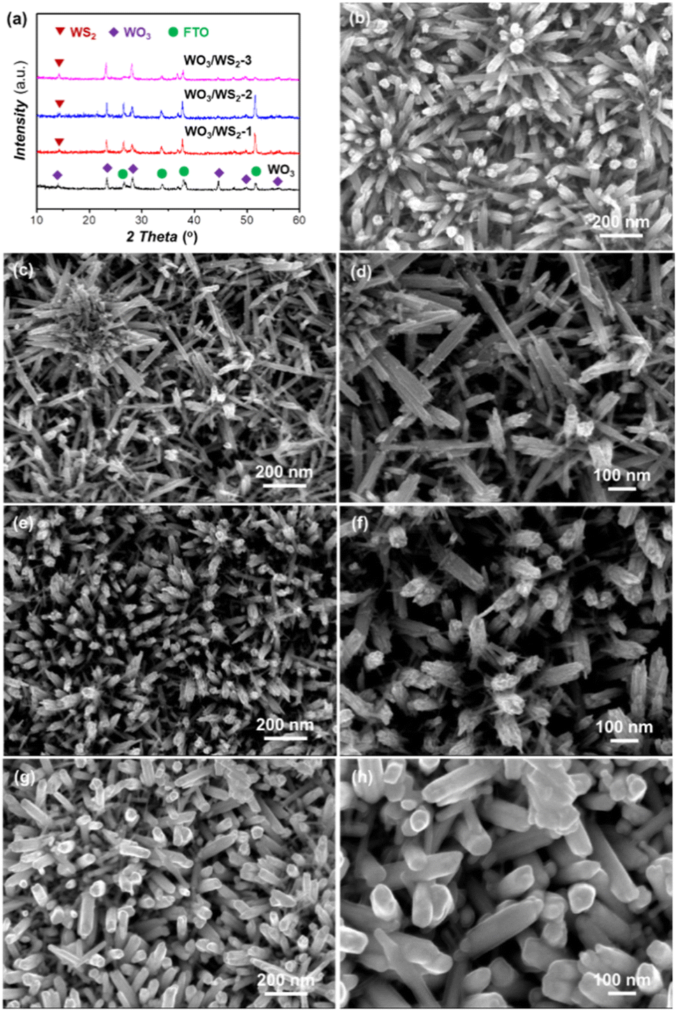 | ||
| Fig. 1 (a) XRD patterns of pristine and sulfurized WO3 nanowire arrays. (b) Top view SEM images of WO3 nanowire arrays grown at 180 °C for 15 h (c, e and g). Top view SEM images of WO3/WS2 nanowire arrays synthesized at 180 °C for 5 h, 10 h and 15 h (d, f and h). High-resolution SEM images of WO3/WS2 nanowire arrays synthesized at 180 °C for 5 h, 10 h and 15 h. | ||
In order to obtain the microcrystal structure and surface information of WO3/WS2 core–shell nanowire arrays, the TEM measurements were carried out. As shown in Fig. 2a, which exhibits a low-magnification TEM image of WO3/WS2 core–shell nanowire arrays, a clear regular shape could be observed. In Fig. 2b and c, a clear interface between the core WO3 and shell WS2 could be observed from the high-resolution transmission electron microscopy (HRTEM) images, revealing the intimate combination of the core/shell structure. The WS2 shell thickness was measured to be 13 nm. Fig. 2c shows an interplanar distance of 0.38 nm, which is consistent with the (002) crystal plane distance of WO3. The interplanar distance of the shell was measured to be 0.15 nm, which matches well with the (008) plane of WS2. This good lattice match between the core and shell is beneficial to decrease the combination possibility in the bulk and promote the charge transport between the WO3 and WS2 interface.
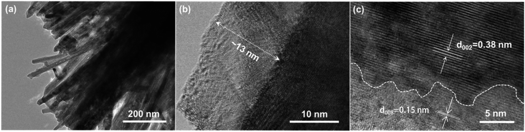 | ||
| Fig. 2 Structural characterization of the WO3-based nanowire arrays. (a) TEM image of the WO3/WS2 nanowire arrays. (b and c) HRTEM images of individual WO3/WS2 core–shell nanowire. | ||
To further survey the elements distribution of the WO3/WS2 core–shell structure, an individual nanowire was characterized by HRTEM coupled with energy dispersive X-ray spectroscopy (EDS). Fig. 3a shows the HRTEM image of a single nanowire and Fig. 3b–d shows the corresponding elemental map of O, S, and W. It is obvious that W and O elements have higher signals, also indicating relative uniform distribution across the nanowire. The presence of the signal of the S element further confirms the formation of the WO3/WS2 core–shell structure.
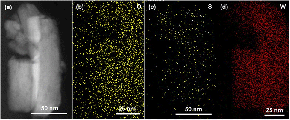 | ||
| Fig. 3 (a) HRTEM image of WO3/WS2 core–shell nanowire prepared at 180 °C for 15 h. (b–d) EDS of the selected area. | ||
In order to explicate the chemical composition of the nanowire arrays, XPS measurements were performed. Fig. 4 displays the high-resolution XPS spectra of W and S elements. As seen in Fig. 4a, the binding energy of the W 4f7/2 and W 4f5/2 appear at 35.7 eV and 37.8 eV, which are consistent with the values of bare WO3 from the relevant literature.17,28,29 The differentiation between W 4f7/2 and W 4f5/2 was about 2.1 eV, indicating the typical binding energy of W6+. Nevertheless, there is a shift in the binding energy of W 4f after sulfurization. The peaks for W 4f7/2 and W 4f5/2 were observed at 32.58 eV and 35.58 eV, respectively, suggesting the existence of the tetravalent tungsten.23 Fig. 4b shows the XPS results of S 2p, the signal of S 2p could not be found in pure WO3. However, the peak of S 2p was observed after sulfurization. The fine spectrum of S 2p in the sulfurized WO3 showed two different peaks at 162.21 eV and 163.28 eV, which are attributed to the S 2p3/2 and S 2p1/2, respectively, of S–W in WS2.22,30 Combining the aforementioned results, we could acknowledge the successful synthesis of WO3/WS2 core–shell structure.
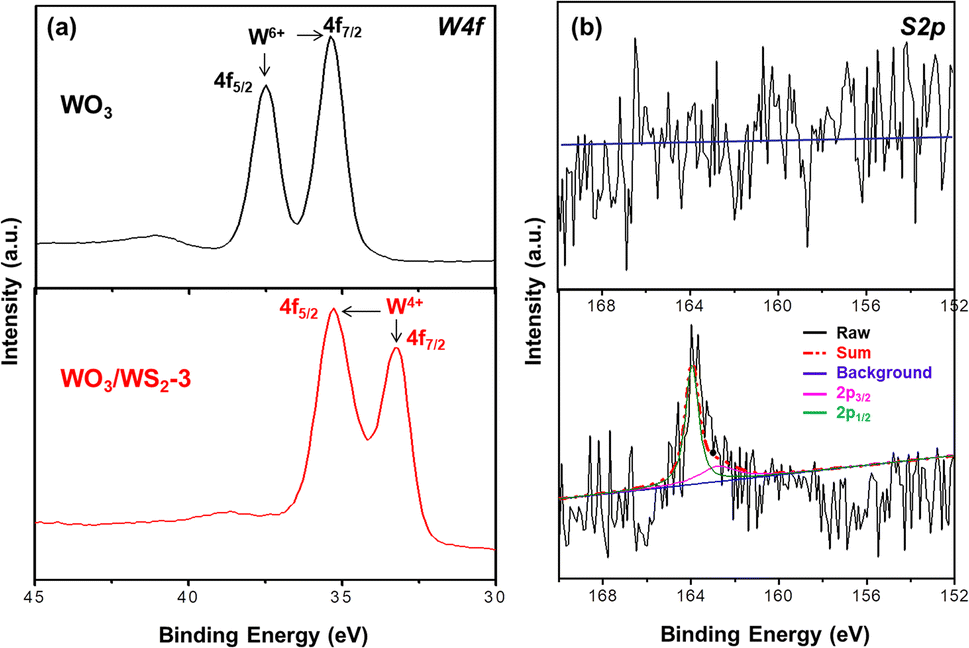 | ||
| Fig. 4 High resolution XPS spectra of (a) W 4f peak and (b) S 2p peak of the samples. Top: pure WO3; bottom: WO3/WS2 core–shell nanowire. | ||
3.2 Photoelectrochemical properties of the WO3/WS2 core–shell structure photoanode
The optical properties of WO3 and WO3/WS2 core–shell nanowire arrays were characterized using UV-vis. As depicted in Fig. 5a, the pure WO3 has an absorption edge at 445 nm. Compared with pristine WO3, a red shift was observed in the WO3/WS2 samples, which is due to the formation of a narrow band gap WS2 on the surface of WO3. According to the Kubelka–Munk equation, the band gap of a semiconductor could be calculated:| αhv = A(hv − Eg)n/2 |
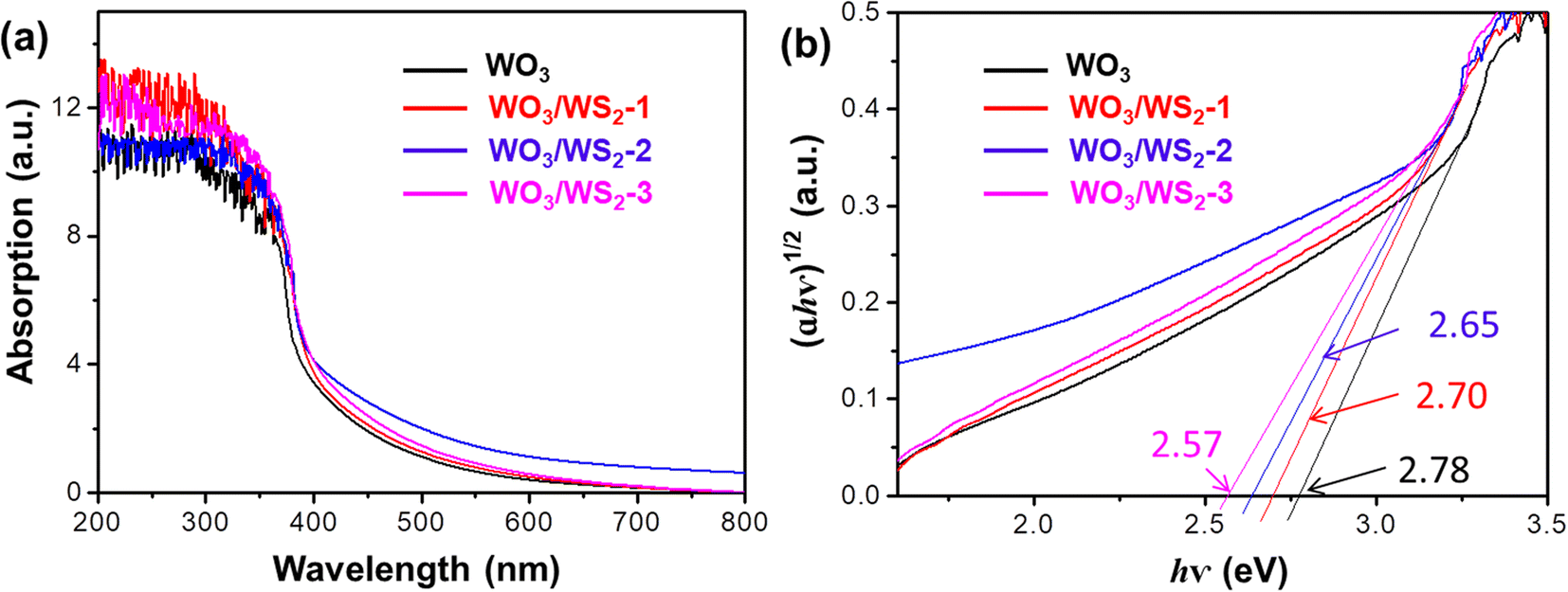 | ||
| Fig. 5 (a) UV-vis spectra and (b) plots of the (αhν)1/2 vs. photon energy (hν) of WO3 and WO3/WS2 core–shell nanowire arrays synthesized at 180 °C for 5 h, 10 h and 15 h (WO3/WS2-1, 2 and 3). | ||
The photoelectrochemical (PEC) properties of WO3 and WO3/WS2 nanowires were evaluated by measuring the photocurrent density at 1.23 V (vs. revisable hydrogen electrode, RHE) in 1 M NaOH solution. As shown in Fig. 6a, the photocurrent density (Jph) of the bare WO3 nanowire was 0.43 mA cm−2 (at 1.23 V vs. RHE). After sulfurization, the WO3/WS2 nanowire prepared at 180 °C for 15 h showed the highest Jph (0.91 mA cm−2), increased by 112% compared with bare WO3. The Jph of WO3/WS2 nanowires fabricated at 180 °C for 5 h and 10 h were 0.58 mA cm−2 and 0.81 mA cm−2, respectively, which is still larger than that of pure WO3. The large increase in the photocurrent density shows that the core–shell structure greatly improves the PEC properties of WO3. The enhanced light absorption of the WS2 shell, as proved in Fig. 5, could be one of the reasons, but cannot fully explain such a large increase in performance. In the next section, we analyzed its energy band mechanism to explain this phenomenon.
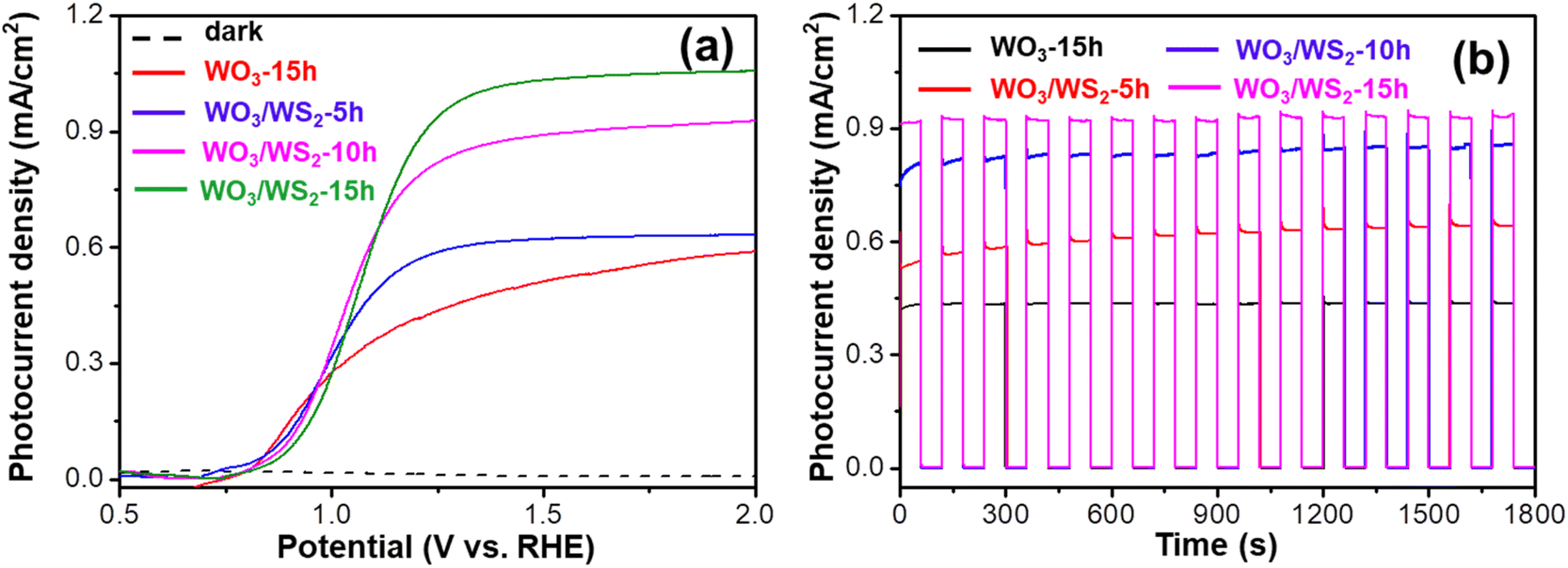 | ||
| Fig. 6 Photoelectrochemical measurements of pristine WO3 and WO3/WS2 core–shell nanowire arrays synthesized at 180 °C for 5 h, 10 h and 15 h (a) photocurrent density–potential (Jph–V) curves and (b) chronoamperometry plots in 1800 s. Measured in 1 M NaOH under AM 1.5 G illumination. | ||
Apart from the excellent PEC performance, the stability of the photoanode is very crucial for practical applications. The chronoamperometry measurements were performed to investigate the stability of WO3 and WO3/WS2 nanowire arrays. As seen in Fig. 6b, the Jph of all samples remained the same during the entire experiment and showed no degradation tendency, suggesting that WO3/WS2 nanowiress have good stability as well as an anti-photo corrosion ability. Furthermore, the samples exhibited a quick photoresponse during the light chopping, which meant a more efficient charge separation and transportation at the WO3/WS2 interface due to the construction of the heterostructure.
3.3 Photocatalytic mechanism of the WO3/WS2 core–shell structure photoanode
Seo et al.24 and Lee et al.25 reported WO3/WS2 nanowires structured Z-scheme heterojunction, and the schematic diagram of the energy band structure as shown in Fig. 7. As the shell of the thickness of WS2 was approximately 13 nm, both WO3 and WS2 could be excited. Excited electrons and holes are generated in the conduction and valence bands of WO3 and WS2, respectively. Since the VBM of WS2 is higher than that of WO3, the electrons flowed from WS2 to WO3 spontaneously.7 Similarly, holes spontaneously flowed from WO3 to WS2. Therefore, positive and negative charges are concentrated on the WS2 and WO3 surfaces. Then, the electrons were transferred to a counter electrode via the back contact, and an external circuit was used in the reduction reactions. As a result, the heterojunction of WO3/WS2 not only efficiently separated the photogenerated electron–hole pairs but also effectively transported electrons and holes into the cathode and anode for the hydrogen- and oxygen-evolution reactions, respectively.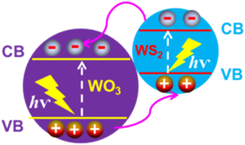 | ||
| Fig. 7 Schematic illustration of the energy band alignment of WO3@WS2 core–shell for photoelectrochemical water splitting. | ||
The PEC water splitting performance was governed by many factors, including the phase structure, light absorption ability, separation and transportation efficiency of photoexcited charges, and stability. Combining the XRD and SEM results, the synthesized nanowire arrays show good crystallinity. The TEM and XPS results confirmed the good contact between the WS2 shell and WO3 core, which facilitated the charge transportation. The shell WS2 with a narrower band gap, as demonstrated in Fig. 5, enhanced the light absorption.
Therefore, it can be concluded that the WO3/WS2 core–shell formed a heterostructure, which not only boosted the light response but also accelerated the separation as well as the transportation of photogenerated charges for efficient PEC water splitting.
4. Conclusion
In summary, uniform WO3/WS2 core–shell nanowire arrays were synthesized by a simple hydrothermal method. The highest photocurrent density of the WO3/WS2 (15 h) nanowire was 0.91 mA cm−2 (at 1.23 V vs. RHE), while pure WO3 only reached 0.43 mA cm−2. Besides, all the samples showed excellent stability under illumination. The enhanced photoelectrochemical performance was due to the formation of a WS2 shell on the surface of WO3, which enhances light absorption ability as well as the charge separation and transportation of the photoanode. The successful synthesis of WO3/WS2 core–shell nanowires by sulfurization paves a new path for the design of narrow-band gap water-splitting materials with high stability.Conflicts of interest
There are no conflicts to declare.Acknowledgements
This work is supported by Henan Power Battery Innovation Center Co., Ltd and the Science and Technology Commission of Shanghai (No. 17010500600).References
- M. Gratzel, Photoelectrochemical cells, Nature, 2001, 414, 338–344 CrossRef CAS PubMed.
- C. Jiang, S. J. A. Moniz, A. Wang, T. Zhang and J. Tang, Photoelectrochemical devices for solar water splitting – materials and challenges, Chem. Soc. Rev., 2017, 46, 4645–4660 RSC.
- P. Lianos, Review of recent trends in photoelectrocatalytic conversion of solar energy to electricity and hydrogen, Appl. Catal., B, 2017, 210, 235–254 CrossRef CAS.
- M. G. Walter, E. L. Warren, J. R. McKone, S. W. Boettcher, Q. X. Mi, E. A. Santori and N. S. Lewis, Solar Water Splitting Cells, Chem. Rev., 2010, 110, 6446–6473 CrossRef CAS PubMed.
- A. Fujishima and K. Honda, Electrochemical photolysis of water at a semiconductor electrode, Nature, 1972, 238, 37–38 CrossRef CAS PubMed.
- F. E. Osterloh, Inorganic materials as catalysts for photochemical splitting of water, Chem. Mater., 2008, 20, 35–54 CrossRef CAS.
- T. Hisatomi, J. Kubota and K. Domen, Recent advances in semiconductors for photocatalytic and photoelectrochemical water splitting, Chem. Soc. Rev., 2014, 43, 7520–7535 RSC.
- K. Sivula and R. van de Krol, Semiconducting materials for photoelectrochemical energy conversion, Nat. Rev. Mater., 2016, 1, 15010 CrossRef CAS.
- P. Dias, T. Lopes, L. Meda, L. Andrade and A. Mendes, Photoelectrochemical water splitting using WO3 photoanodes: the substrate and temperature roles, Phys. Chem. Chem. Phys., 2016, 18, 5232–5243 RSC.
- G. Zheng, J. Wang, H. Liu, V. Murugadoss, G. Zu, H. Che, C. Lai, H. Li, T. Ding, Q. Gao and Z. Guo, Tungsten oxide nanostructures and nanocomposites for photoelectrochemical water splitting, Nanoscale, 2019, 11, 18968–18994 RSC.
- Y. Wang, W. Tian, C. Chen, W. Xu and L. Li, Tungsten Trioxide Nanostructures for Photoelectrochemical Water Splitting: Material Engineering and Charge Carrier Dynamic Manipulation, Adv. Funct. Mater., 2019, 29, 1809036 CrossRef.
- S. S. Kalanur, Y. J. Hwang, S. Y. Chae and O. S. Joo, Facile growth of aligned WO3 nanorods on FTO substrate for enhanced photoanodic water oxidation activity, J. Mater. Chem. A, 2013, 1, 3479–3488 RSC.
- J. Zhang, Z. Liu and Z. Liu, Novel WO3/Sb2S3 Heterojunction Photocatalyst Based on WO3 of Different Morphologies for Enhanced Efficiency in Photoelectrochemical Water Splitting, ACS Appl. Mater. Interfaces, 2016, 8, 9684–9691 CrossRef CAS PubMed.
- S. Wang, H. Chen, G. Gao, T. Butburee, M. Lyu, S. Thaweesak, J.-H. Yun, A. Du, G. Liu and L. Wang, Synergistic crystal facet engineering and structural control of WO3 films exhibiting unprecedented photoelectrochemical performance, Nano Energy, 2016, 24, 94–102 CrossRef CAS.
- G. Zheng, J. Wang, H. Li, Y. Li and P. Hu, WO3/Cu2O heterojunction for the efficient photoelectrochemical property without external bias, Appl. Catal., B, 2020, 265, 118561 CrossRef CAS.
- S. Zhang, J. Wang, S. Chen, R. Li and T. Peng, Construction of Ag2S/WO3 Direct Z-Scheme Photocatalyst for Enhanced Charge Separation Efficiency and H2 Generation Activity, Ind. Eng. Chem. Res., 2019, 58, 14802–14813 CrossRef CAS.
- L. Huang, H. Xu, Y. Li, H. Li, X. Cheng, J. Xia, Y. Xu and G. Cai, Visible-light-induced WO3/g-C3N4 composites with enhanced photocatalytic activity, Dalton Trans., 2013, 42, 8606–8616 RSC.
- J. Su, L. Guo, N. Bao and C. A. Grimes, Nanostructured WO3/BiVO4 Heterojunction Films for Efficient Photoelectrochemical Water Splitting, Nano Lett., 2011, 11, 1928–1933 CrossRef CAS PubMed.
- B. R. Lee, M. G. Lee, H. Park, T. H. Lee, S. A. Lee, S. S. M. Bhat, C. Kim, S. Lee and H. W. Jang, All-Solution-Processed WO3/BiVO4 Core–Shell Nanorod Arrays for Highly Stable Photoanodes, ACS Appl. Mater. Interfaces, 2019, 11, 20004–20012 CrossRef CAS PubMed.
- F. Zhan, J. Li, W. Li, Y. Liu, R. Xie, Y. Yang, Y. Li and Q. Chen, In situ formation of CuWO4/WO3 heterojunction plates array films with enhanced photoelectrochemical properties, Int. J. Hydrogen Energy, 2015, 40, 6512–6520 CrossRef CAS.
- A. A. Markhabayeva, M. Moniruddin, R. Dupre, K. A. Abdullin and N. Nuraje, Designing of WO3@Co3O4 Heterostructures to Enhance Photoelectrochemical Performances, J. Phys. Chem. A, 2020, 124, 486–491 CrossRef CAS PubMed.
- M. S. Akple, J. Low, S. Wageh, A. A. Al-Ghamdi, J. Yu and J. Zhang, Enhanced visible light photocatalytic H2-production of g-C3N4/WS2 composite heterostructures, Appl. Surf. Sci., 2015, 358, 196–203 CrossRef CAS.
- X. Wang, G. Hai, B. Li, Q. Luan, W. Dong and G. Wang, Construction of dual-Z-scheme WS2-WO3·H2O/g-C3N4 catalyst for photocatalytic H2 evolution under visible light, Chem. Eng. J., 2021, 426, 130822 CrossRef CAS.
- D.-B. Seo, S. Yoo, V. Dongquoc, T. N. Trung and E.-T. Kim, Facile synthesis and efficient photoelectrochemical reaction of WO3/WS2 core@shell nanorods utilizing WO3·0.33H2O phase, J. Alloys Compd., 2021, 888, 161587 CrossRef CAS.
- N. Lee, I. Y. Choi, K.-Y. Doh, J. Kim, H. Sim, D. Lee, S.-Y. Choi and J. K. Kim, Enhanced catalytic activity of edge-exposed 1T phase WS2 grown directly on a WO3 nanohelical array for water splitting, J. Mater. Chem. A, 2019, 7, 26378–26384 RSC.
- J. Zhang, J.-p. Tu, X.-h. Xia, X.-l. Wang and C.-d. Gu, Hydrothermally synthesized WO3 nanowire arrays with highly improved electrochromic performance, J. Mater. Chem., 2011, 21, 5492–5498 RSC.
- P. M. Rao, L. Cai, C. Liu, I. S. Cho, C. H. Lee, J. M. Weisse, P. Yang and X. Zheng, Simultaneously Efficient Light Absorption and Charge Separation in WO3/BiVO4 Core/Shell Nanowire Photoanode for Photoelectrochemical Water Oxidation, Nano Lett., 2014, 14, 1099–1105 CrossRef CAS PubMed.
- G. Lu, X. Li, Z. Qu, Q. Zhao, H. Li, Y. Shen and G. Chen, Correlations of WO3 species and structure with the catalytic performance of the selective oxidation of cyclopentene to glutaraldehyde on WO3/TiO2 catalysts, Chem. Eng. J., 2010, 159, 242–246 CrossRef CAS.
- L. Jiang, X. Yuan, G. Zeng, J. Liang, X. Chen, H. Yu, H. Wang, Z. Wu, J. Zhang and T. Xiong, In-situ synthesis of direct solid-state dual Z-scheme WO3/g-C3N4/Bi2O3 photocatalyst for the degradation of refractory pollutant, Appl. Catal., B, 2018, 227, 376–385 CrossRef CAS.
- D. Lin, Y. Zhou, X. Ye and M. Zhu, Construction of sandwich structured photocatalyst using monolayer WS2 embedded g-C3N4 for highly efficient H2 production, Ceram. Int., 2020, 46, 12933–12941 CrossRef CAS.
| This journal is © The Royal Society of Chemistry 2023 |