
 Open Access Article
 This Open Access Article is licensed under a Creative Commons Attribution-Non Commercial 3.0 Unported Licence
Facile synthesis of Si/Ge/graphite@C composite with improved tap density and electrochemical performance†
Ling Changa,
Yan Linb,
Kai Wang *a,
Ruiqiang Yana,
Wei Chena,
Zecong Zhaoa,
Yanping Yanga,
Guobo Huang*a,
Wei Chenc,
Jian Huangc and
Youzhi Song*d
*a,
Ruiqiang Yana,
Wei Chena,
Zecong Zhaoa,
Yanping Yanga,
Guobo Huang*a,
Wei Chenc,
Jian Huangc and
Youzhi Song*d
aSchool of Pharmaceutical and Chemical Engineering, Taizhou University, Taizhou 318000, China
bZhejiang Provincial Key Laboratory for Cutting Tools, Taizhou University, Taizhou 318000, China
cERA Co., Ltd, Taizhou 318000, China
dKey Laboratory of Macromolecular Synthesis and Functionalization (Ministry of Education), International Research Central for Functional Polymers, Department of Polymer Science and Engineering, Zhejiang University, Hangzhou 310027, China
First published on 21st December 2022
Abstract
Nanoengineering is one of the most effective methods to promote the lithium storage performance of silicon material, which suffers from huge volume changes and poor reaction kinetics during cycling. However, the commercial application of nanostructured silicon is hindered by its high manufacturing cost and low tap density. Herein, a Si/Ge/graphite@C composite was successfully synthesized by ball-milling with subsequent calcination. By introducing Ge, graphite and an amorphous carbon coating, both tap density and electrochemical performance are improved significantly. Benefiting from the synergetic effects of the above components, the Si/Ge/graphite@C composite delivers a reversibility capacity of 474 mA h g−1 at 0.2 A g−1 and stable capacity retention.
1. Introduction
With the increasing concern of CO2 emission and environmental deterioration, energy storage devices such as lithium ion batteries (LIBs) have been widely used for the storage and utilization of renewable energy.1–4 Due to its high theoretical capacity and low working potential, silicon is considered as one of the ideal anode materials for next generation LIBs with high energy density.5–7 However, it suffers from severe volume changes during the alloying/dealloying process which leads to the mechanical fracture of particles and pulverization of electrodes. Eventually, these defects lead to rapid decay of capacity and low coulomb efficiency. Besides, the low electronic conductivity and poor lithium ion diffusion of Si also limit its practical application.8–10To address the above problems, one of the most effective strategies is nanoengineering. By reducing the size of silicon material to the nanoscale, it can effectively buffer the internal stress during cycling and shorten lithium ion diffusion distance.11,12 Based on this theory, various nanostructured silicon materials have been successfully fabricated, such as nanowires,13 nanotubes,14 hollow or porous particles.15,16 All of them showed improved cycle stability and rate performance to a certain extent. Nevertheless, complex manufacturing, high cost and low tap density make it difficult to meet practical applications. Meanwhile, during the initial formation of the solid electrolyte interface (SEI), the huge specific surface area brings more irreversible capacity loss, leading to the waste of cathode materials in full cells.17–20
Another method to improve the lithium storage performance of silicon is to prepare silicon based composites.21–24 Carbon materials including graphite, graphene and amorphous carbon have been widely applied because of their excellent electrical and mechanical properties.25–27 The conventional anode graphite has a much smaller volume expansion (∼10%) and more stable electrode/electrolyte interface than silicon. Thus, the material composed of silicon and graphite usually exhibits better structural integrity during cycling. Moreover, certain metal like germanium is gifted with better electronic conductivity and ion diffusion rate. When introduced to silicon composite, it can effectively promote reaction kinetics and reduce internal polarization. It has been demonstrated that the initial coulomb efficiency can be dramatically promoted when silicon is compounded with germanium or tin.28–30 However, it is still necessary to explore the preparation technology of silicon based composites suitable for industrial large-scale production.
Herein, we report the reasonable design and successful fabrication of Si/Ge/graphite@C anode material. Considering the application economy, both raw materials and manufacturing techniques are common and low-cost. Micro silicon was ball milled into the composite to raise the mass specific capacity. Meanwhile, little amount of Ge was introduced to improve electrochemical reaction kinetics. In order to promote the tap density, graphite with flake morphology was added by the same way. Besides, gelatin was used as glue to form secondary particles and further decomposed to carbon coating layer, which enhanced the electronic conductivity and interface stability. As a result, the unique composition and structure provide a synergistic effect of improving overall performances. When served as the anode material of LIBs, the Si/Ge/graphite@C shows higher initial coulomb efficiency, capacity retention and better rate performance. Furthermore, the lithiation/delithiation mechanism and pseudo capacitance contribution are investigated through cyclic voltammetry technology.
2. Experimental
2.1 Materials
Silicon powder (200 mesh, AR, 99.9%), germanium dioxide (AR, 99.9%), flake graphite (AR, 99.9%) and gelatin (LR, 98%) were purchased from Sinopharm Chemical Reagent Co., Ltd.2.2 Synthesis of Si/Ge composites
Si (1.685 g) and GeO2 (0.419 g) with a molar ratio of 15![[thin space (1/6-em)]](https://www.rsc.org/images/entities/char_2009.gif) :1 were ground in 12 cycles of 30 min of ball-milling with 15 min breaks between each cycle in a 100 mL ZrO2 grinding jar with a planetary ball mill (Nanjing University Instrument Factory), the ball-milling rotation rate was 400 rpm and the mass ratio of ZrO2 grinding balls and the powder (Si and GeO2) was 20:1. Then, the obtained materials were sintered under Ar/H2 (95/5, v/v) atmosphere at 900 °C for 2 h with a heating rate of 3 °C min−1 (the sintering furnace type: OTF-1200X, HF-kejing. The diameter of the quartz tube is 50 mm and the size of the porcelain boat is 60 × 30 mm). After cooling down to room temperature (first, cooling down to 400 °C with a cooling rate of 5 °C min−1, then cooling down to room temperature naturally), a brown powder (Si/Ge composites) was collected. For comparison, pure micro Si powder was treated in the same condition as above except adding GeO2.
:1 were ground in 12 cycles of 30 min of ball-milling with 15 min breaks between each cycle in a 100 mL ZrO2 grinding jar with a planetary ball mill (Nanjing University Instrument Factory), the ball-milling rotation rate was 400 rpm and the mass ratio of ZrO2 grinding balls and the powder (Si and GeO2) was 20:1. Then, the obtained materials were sintered under Ar/H2 (95/5, v/v) atmosphere at 900 °C for 2 h with a heating rate of 3 °C min−1 (the sintering furnace type: OTF-1200X, HF-kejing. The diameter of the quartz tube is 50 mm and the size of the porcelain boat is 60 × 30 mm). After cooling down to room temperature (first, cooling down to 400 °C with a cooling rate of 5 °C min−1, then cooling down to room temperature naturally), a brown powder (Si/Ge composites) was collected. For comparison, pure micro Si powder was treated in the same condition as above except adding GeO2.
2.3 Synthesis of Si/Ge/graphite composites
The Si/Ge/graphite (Si/Ge/G) composites were obtained by a similar procedure except that the flake graphite (2.1 g) was added in the ball-milling process. The grinded product was also calcined at 900 °C for 2 h under an Ar/H2 (95/5, v/v) atmosphere.2.4 Synthesis of Si/Ge/graphite@C composites
1.0 g gelatin was dissolved in 50 mL deionized H2O under continuous stirring at 60 °C for 10 min. After completely dissolved, 1.0 g Si/Ge/graphite was added to the above solution and stirred for 20 min. Then, the mixture was totally dried at 80 °C in an oven. The Si/Ge/graphite@C composites were finally obtained by annealing the solid under an Ar/H2 (95/5, v/v) atmosphere at 900 °C for 2 h.2.5 Characterization
The phase structure and crystal type of the materials were characterized by powder X-ray diffraction (XRD, SmartLab SE, 40 kV, 40 mA) with Cu Kα radiation. Raman spectra was recorded using HR RamLab with the excitation source of 532 nm. The morphologies and microstructure were characterized by scanning electron microscope (SEM, Hitachi S4800) and transmission electron microscopy (TEM, JEOL JEM 2100F). The X-ray photoelectron spectroscopy (XPS, Thermo Scientific K-Alpha, Al Kα, 12 kV, 6 mA) was used to analyze the surface composition, and the spectra were revised by the C 1s peak at a binding energy of 284.8 eV. Brunauer–Emmett–Teller (BET) surface areas were measured using a Micrometrics ASAP 2010 instrument. Thermogravimetric analysis (TGA) was conducted to analyze the contents of the final composite.2.6 Electrochemical measurements
The electrochemical performances of the composites were conducted by assembling CR2016-type coin cells in an Ar-filled glove box with H2O and O2 content less than 1 ppm. The active material (Si, Si/Ge, Si/Ge/graphite and Si/Ge/graphite@C), acetylene black (LITX) and poly(vinylidene fluoride) (PVDF) were mixed with a mass ratio of 70:15:15 and grinded evenly. Then, a moderate amount of N-methylpyrrolidone (NMP) was added to the above mixture drop by drop under the infrared lamp to adjust the viscosity. A black slurry was finally obtained after vigorous stirring for a certain time. The working electrode was prepared by casting the slurry on Cu foil, followed by drying at 80 °C in a vacuum oven for 12 h. The electrodes before assembling are extruded through a double-roll machine. Li foil was used as the counter and reference electrode and polypropylene membrane (Celgard 2325) was employed as the separator. 1 M LiPF6 dissolved in ethylene carbonate (EC)/dimethyl carbonate (DMC) (1:1, v/v) was used as the electrolyte. Galvanostatic charge–discharge and rate performances were tested using a Neware battery test system with a cut-off voltage range of 0.01–2.0 V (vs. Li/Li+). Cyclic voltammetry (CV) was performed on a CHI 760E electrochemical workstation from 0.01 to 2.0 V with a scanning rate of 0.2 mV s−1. The EIS was carried out in the frequency range of 100 kHz to 0.01 Hz with the amplitude of 5 mV. The specific capacities were calculated based on the total mass of the active materials. The average mass loading of the Si/Ge/graphite@C composite material on the Cu substrate was ∼1.5 mg cm−2. The thickness of the coating layer is ∼13 μm.
3. Results and discussion
As illustrated in Fig. 1, micro silicon and GeO2 are ball-milled to nanoscale particles firstly. Then, flake graphite was added into the tank and ball-milled again to form a uniform mixture. After sieved, the Si/GeO2/graphite composite was collected and stirred in the gelatin solution. Finally, the Si/Ge/graphite@C secondary particles were obtained after a high temperature annealing in a tube furnace filled with Ar/H2.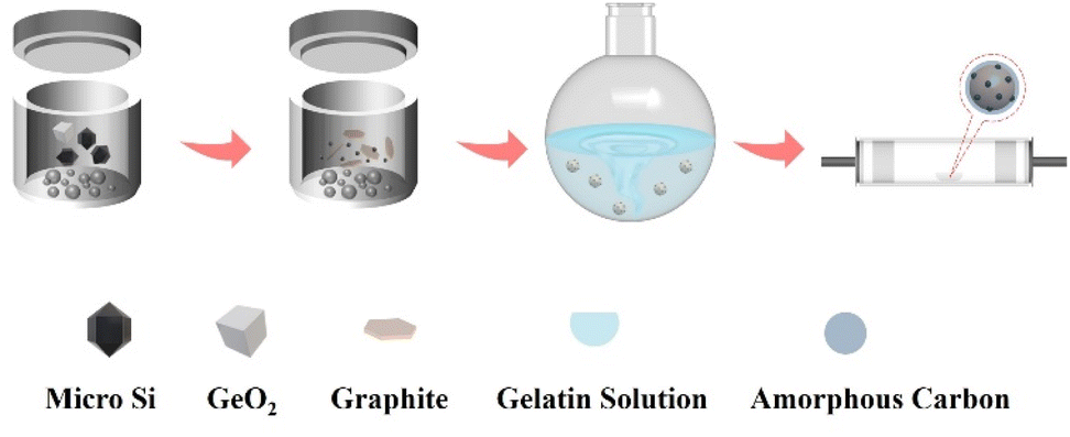 | ||
| Fig. 1 Illustration of the synthesis of Si/Ge/graphite@C. | ||
The morphologies and microstructures of the as-synthesized samples were studied by scanning electron microscopy (SEM) and transmission electron microscopy (TEM), respectively. Fig. 2a shows the morphology of ball-milled Si, displaying that spherical particles with the diameter of 100–300 nm are finally obtained. As demonstrated in Fig. 2b, the size and shape of the acquired Si/Ge composite are similar with the ball-milled Si. The image of Si/Ge/graphite in Fig. 2c exhibits that the Si/Ge particles are well distributed on the graphite surface after ball-milling. Fig. 2d–f shows the Si/Ge/graphite@C images with different magnifications. As can be seen, a compact structure is obtained after carbon coating and the Si/Ge particles were tightly connected with graphite (Fig. 2e and f). The element mapping results of Fig. 2d further demonstrates the unique structure of Si/Ge/graphite@C composite (Fig. S1, ESI†). Benefitting from this structure, the carbon coating can not only effectively alleviate the volume expansion of nano Si, but also maintain the integrity of the electrode during the charge/discharge process. Moreover, adding graphite can improve the cycle stability of the Si-based composite. Fig. 2g–i displays the TEM and HRTEM images of Si/Ge/graphite@C. The Si and Ge nanoparticles are well distributed on the graphite surface without agglomeration (Fig. 2g). The high-resolution TEM image in Fig. 2h shows two types of lattice fringes, which can be ascribed to Si (111) and graphite (002) planes, respectively.31,32 Besides, the lattice fringes with the distance of 0.326 nm in Fig. 2i are well-matched to the (111) crystal planes of Ge.33 Furthermore, an amorphous carbon layer coated on the composite can be observed in the inset image of Fig. 2i.
 | ||
| Fig. 2 SEM images of ball-milled Si (a), Si/Ge (b), Si/Ge/G (c) and Si/Ge/graphite@C (d–f), TEM (g) and HRTEM (h and i) of Si/Ge/graphite@C composite. | ||
The tap density is directly related to the volumetric energy density of the materials. Commercial anode material BFC-Q4 (artificial graphite with the tap density ≥ 1.0 g cm−3) was purchased from BTR New Materials Group Co., Ltd for comparison. As shown in Fig. 3, 0.5 g ball-milled Si (nano Si), Si/Ge, Si/Ge/graphite@C composite and BFC-Q4 were put into four cylindrical glass bottle, respectively. The tap density of the samples is calculated according to the following formula:
| Pr = M/V | (1) |
 | ||
| Fig. 3 Photographs of ball-milled Si (nano Si), Si/Ge, Si/Ge/graphite@C composite and artificial graphite (BFC-Q4). | ||
The crystal and phase structure of the as-synthesized samples were characterized by X-ray diffraction (XRD), as shown in Fig. 4a. Three diffraction peaks observed at 28.4°, 47.3° and 56.1° (labeled as “⊙”) in the curve of ball-milled Si can be assigned to the (111), (220) and (311) crystal planes of Si (PDF #27-1402). The other diffraction peaks at 27.3°, 45.3° and 53.6° in the Si/Ge composite (labeled as “☆”) can be attributed to the (111), (220) and (311) crystal planes of Ge (PDF #04-0545). Notably, three peaks at around 26.4°, 44.4° and 54.5° appear in both Si/Ge/graphite and Si/Ge/graphite@C composites, which are the characterization peaks of graphite (labeled as “★”, PDF #41-1487) and are assigned to the (002), (101) and (004) crystal planes.31,33–35 In addition, no impurity is detected, demonstrating that GeO2 is totally reduced after annealing in Ar/H2 atmosphere. The diffraction peaks of Si/Ge/graphite and Si/Ge/graphite@C are basically the same, implying that the carbon derived from gelatin maybe amorphous. Fig. 4b shows the Raman spectra of the Si/Ge/graphite@C composite, the typical bands at 520 cm−1 corresponds to crystalline Si, while the weak peak at 290 cm−1 is assigned to Ge–Ge stretching motions, suggesting the existence of Si and Ge, respectively. The broad peak at 1350 cm−1 (D band) refers to disorder graphite and another peak at 1582 cm−1 (G band) corresponds to crystalline graphite. The 2D band at 2720 cm−1 is formed by two components and it is asymmetric.36,37 The Si, Ge and C contents in the Si/Ge/graphite@C composite are determined via thermogravimetric analysis (TGA), which are calculated to be 20.51%, 3.54% and 75.95%, respectively, as illustrated in Fig. 4c. X-ray photoelectron spectroscopy (XPS) is used to confirm the elemental composition and electronic state. The full spectrum in Fig. 4d shows the distinctive peaks for Si 2p, Ge 3d, C 1s, N 1s and O 1s, which indicates the existence of Si, Ge, C, N and O elements in the Si/Ge/graphite@C composite. The presence of O element maybe owing to the oxidation of Si and Ge and the absorbed oxygen. The high-resolution spectra of Si 2p, Ge 3d, C 1s and N 1s are shown in Fig. S2.† The existence of Si–O (Si4+: 103.7 eV) and Ge–O (32.99 eV) peaks in Fig. S2a and b† are the surface oxidation of Si and Ge, respectively.38,39 The peak of Si–Si (Si0: 99.3 eV) is not apparent, which may be due to the surface oxidation of the sample. The two peaks at around 29.76 and 31.69 eV of Ge 3d spectrum in Fig. S2b† are corresponded to Ge–Ge and Ge–C bands, respectively. The binding energy values of 284, 284.6 and 285.7 eV of C 1s spectrum in Fig. S2c† are ascribed to C–Ge, C![[double bond, length as m-dash]](https://www.rsc.org/images/entities/char_e001.gif) C and C–C, respectively. For the N 1s spectrum, Fig. S2d† indicates three peaks at ∼400.3, 399.5 and 397.6 eV, assignable to graphitic, pyrrolic and pyridinic N, respectively. The formation mechanism of the graphitic, pyrrolic and pyridinic N can be explained as a gradual thermal transformation of N bonding configurations from gelatin.40 Pyrrolic N is first formed when the annealing temperature increases to 400 °C. As the annealing temperature increases gradually (400–500 °C), pyrrolic N is converted to pyridinic N. When the temperature increases to 500 °C and above, pyridinic N can be transformed to graphitic N. Furthermore, the peak intensity of graphitic N is strongest. Graphitic N can enhance the conductivity of carbon. Pyrrolic and pyridinic N can supply more electrochemical reactive active sites, accelerating the diffusion rate of Li+.41 The nitrogen adsorption–desorption isotherms and the pore structure of the Si/Ge/graphite@C composite are shown in Fig. S3.† The specific surface area and the average pore size are 41.98 m2 g−1 and 4.68 nm, respectively, which are calculated by the Brunauer–Emmett–Teller (BET) formula.
C and C–C, respectively. For the N 1s spectrum, Fig. S2d† indicates three peaks at ∼400.3, 399.5 and 397.6 eV, assignable to graphitic, pyrrolic and pyridinic N, respectively. The formation mechanism of the graphitic, pyrrolic and pyridinic N can be explained as a gradual thermal transformation of N bonding configurations from gelatin.40 Pyrrolic N is first formed when the annealing temperature increases to 400 °C. As the annealing temperature increases gradually (400–500 °C), pyrrolic N is converted to pyridinic N. When the temperature increases to 500 °C and above, pyridinic N can be transformed to graphitic N. Furthermore, the peak intensity of graphitic N is strongest. Graphitic N can enhance the conductivity of carbon. Pyrrolic and pyridinic N can supply more electrochemical reactive active sites, accelerating the diffusion rate of Li+.41 The nitrogen adsorption–desorption isotherms and the pore structure of the Si/Ge/graphite@C composite are shown in Fig. S3.† The specific surface area and the average pore size are 41.98 m2 g−1 and 4.68 nm, respectively, which are calculated by the Brunauer–Emmett–Teller (BET) formula.
 | ||
| Fig. 4 (a) XRD patterns of ball-milled Si, Si/Ge, Si/Ge/graphite and Si/Ge/graphite@C. (b) Raman spectra, (c) TGA curves and (d) XPS spectrum of Si/Ge/graphite@C composite. | ||
The electrochemical cycling performances of Si, Si/Ge, Si/Ge/graphite and Si/Ge/graphite@C composites are displayed in Fig. 5a. In comparison, Si/Ge/graphite exhibits a reversible capacity of 287 mA h g−1 after 100 cycles, while Si/Ge/graphite@C composite exhibits a higher capacity of 474 mA h g−1, indicating that N-doped carbon coating derived from gelatin pyrolysis can effectively improve the cyclic stability of the composite. Inversely, the cycling properties of Si and Si/Ge decay rapidly due to large volume expansion during cycling and poor electrical conductivity. Fig. 5b shows the initial coulombic efficiency (ICE) of the as-synthesized materials. Obviously, the ball-milled Si and Si/Ge composite give a lower ICE of 68.9% and 71.1%, which may be due to the larger specific area after ball-milling.42 While the ICE of Si/Ge/graphite@C (79.3%) is improved significantly with the addition of graphite. Meanwhile, adding graphite and subsequent carbon coating can reduce the volume effect of Si and improve the energy density and cycling stability. The rate capabilities of the as-synthesized samples are investigated and presented in Fig. 5c. The Si/Ge/graphite@C composite exhibits the best rate capability, achieving the capacities of 546, 511, 440, 383 and 333 mA h g−1 at current densities of 0.2, 0.5, 1, 1.5 and 2.0 A g−1, respectively. When the current density returns back to 0.2 A g−1, a high specific capacity of 529 mA h g−1 is stilled obtained, revealing outstanding rate performance. In contrast, the rate capability of Si and Si/Ge composite is poor, the capacities decay rapidly. Even when the current density returns back to 0.2 A g−1, the capacity can not be restored, indicating that the structure has been destroyed during the charge–discharge process at high current density. Electrochemical impedance spectroscopy (EIS) measurements are carried out to explore the lithium storage kinetics, as shown in Fig. 5d. The Nyquist plots of the as-synthesized materials contain a semicircle in the high frequency region and a sloping line in the low-frequency region. They can be attributed to the charge transfer resistance (Rct) and diffusion impedance (Zw) of Li+, respectively.43,44 It can be distinctly observed that the Rct of the Si/Ge/graphite@C composite is the smallest among the as-synthesized materials, indicating a faster faradaic reaction kinetics owing to an excellent electrical conductivity after carbon coating. Furthermore, the Zw of the Si/Ge/graphite@C composite is smaller than the Si, Si/Ge and Si/Ge/graphite on account of the straight line with a bigger gradient, illustrating a rapid diffusion rate of Li+. The long-term cycling stability of the Si/Ge/graphite@C composite is also tested, as shown in Fig. 5e. The Si/Ge/graphite@C composite delivers a high capacity of 342 mA h g−1 after 300 cycles at 1 A g−1 with the coulombic efficiency remaining over 99%. It can be attributed to the N-doped carbon coating layer derived from the thermal decomposition of gelatin, which can effectively prevent the pulverization and alleviate volume expansion during the cycling process. Furthermore, the unique composition and structure can accelerate the transport of Li+ and electrons simultaneously. Further, Table S1† shows the comparison of electrochemical properties of the Si/Ge/graphite@C composite and the reported Si-based anodes.
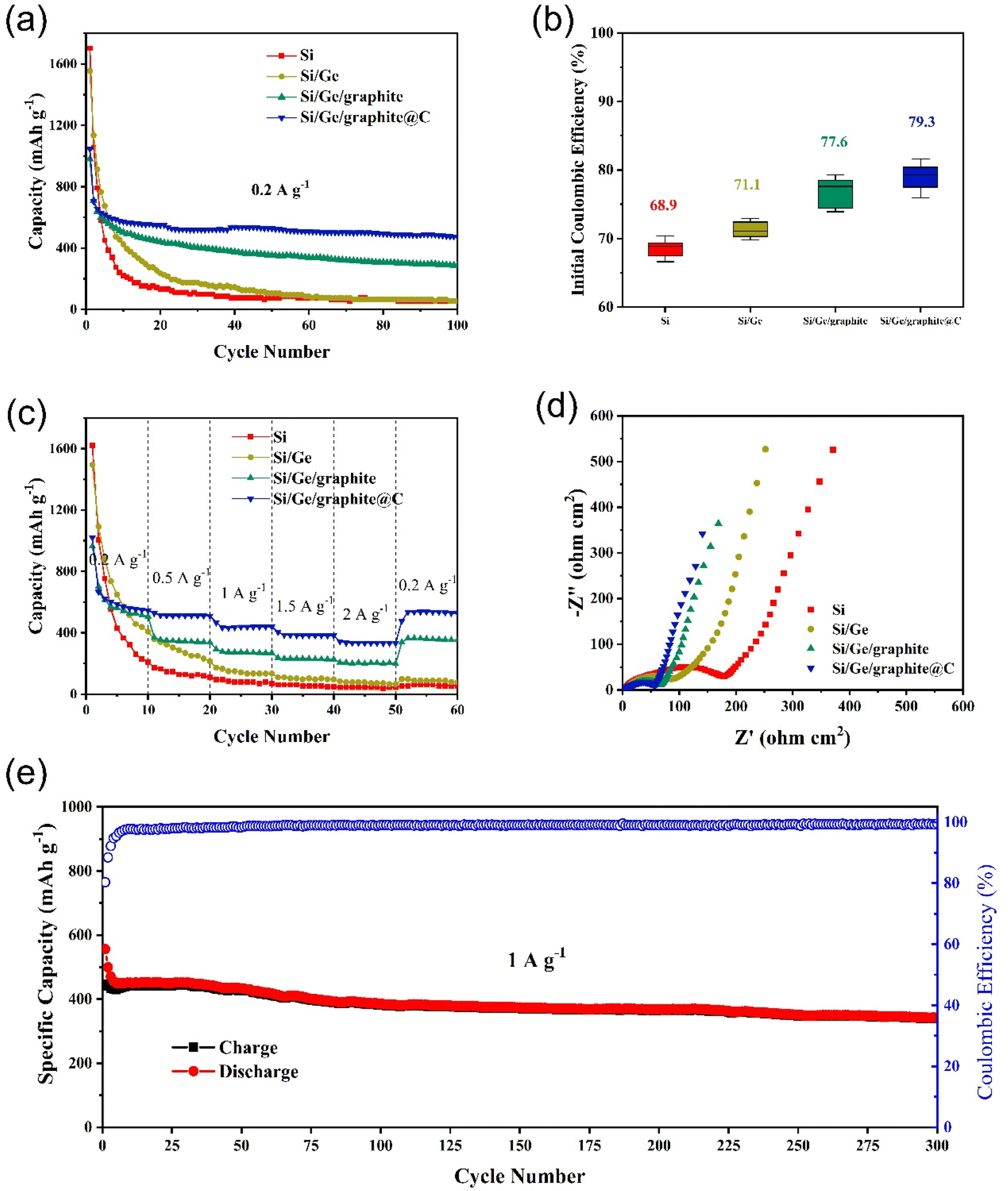 | ||
| Fig. 5 Comparison of cycling performances at 0.2 A g−1 (a), initial coulombic efficiencies (b), rate performances (c) and Nyquist plots of Si, Si/Ge, Si/Ge/graphite and Si/Ge/graphite@C composites (d), respectively. (e) Long-term cycling performance of Si/Ge/graphite@C at 1.0 A g−1. | ||
Fig. 6a demonstrates the cyclic voltammetry (CV) curves of the Si/Ge/graphite@C composite at a scanning rate of 0.2 mV s−1 in the voltage range of 0.01–2.0 V. In the first cycle, a reduction peak at ∼0.7 V is probably ascribed to the formation of solid electrolyte interphase (SEI) film and the peak disappears in the following two cycles, indicating that a steady SEI film is formed.45 Furthermore, the peaks at 0.25 V and below 0.1 V correspond to the lithiation of Ge and Si and the Li+ insertion into graphite. The oxidation peaks at 0.01–0.2 V are assigned to Li+ extraction from graphite. While the oxidation peaks at 0.2–0.3 V and 0.56 V are ascribed to the delithiation of LixSi and LiyGe, respectively.46,47 The current density of CV curves increases continuously in the following two cycles, suggesting an activation process of the Si/Ge/graphite@C composite. The reason for this phenomenon may be attributed to the gradual transformation of silicon from crystal to amorphous structure. As can be seen from Fig. S4,† ex situ XRD results show similar patterns except for different intensities of diffraction peaks. As the number of CV cycles increases, the ratio of Isilicon (2θ at 26.4°) to Igraphite (2θ at 28.4°) decreases continuously. It can be ascribed to the partial transformation from crystal silicon to amorphous phase. In fact, similar phenomena also occurs in germanium anode. In Fig. S4,† the diffraction peaks of germanium have disappeared after the first CV cycle, indicating a total activation process. This is consistent with that the anodic peak current at 0.56 V in Fig. 6a remains unchanged. The charge–discharge profiles of the Si/Ge/graphite@C composite at 0.2 A g−1 are shown in Fig. 6b. The discharge and charge voltage plateaus are in good agreement with the CV results. The discharge and charge capacities of the first three cycles are 1046.6/830.0, 704.6/660.0 and 655.1/638.1 mA h g−1, indicating corresponding coulombic efficiencies of 79.3%, 93.7% and 97.4% respectively. Furthermore, the cumulative capacity loss of the first three cycles is 278.2 mA h g−1. As can be seen in Fig. S5,† the coulombic efficiency has exceeded 99% and maintains stable since the 5th cycle. The initial capacity loss may ascribe to the generation of SEI film. To evaluate the electrochemical kinetics of the lithium storage in the Si/Ge/graphite@C composite, the pseudocapacitive effects are evaluated by CV measurements at a scan rate range of 0.2–2.0 mV s−1, as represented in Fig. 6c. The extent of capacitive effect can be calculated according to the following equations:
| i = aνb | (2) |
|
logi = loga + blogν
| (3) |
i vs. logv plots. Specially, the range of b value is 0.5–1.0. When the value of b approach to 0.5, indicating that a diffusion-controlled behavior dominates the electrochemical reaction kinetics. While b is close to 1.0, manifesting a surface capacitive-dominant mechanism. The values of b are 0.55 and 0.59 for peak 1 and peak 2, respectively, illustrating a diffusion-dominated behavior for the Si/Ge/graphite@C composite.
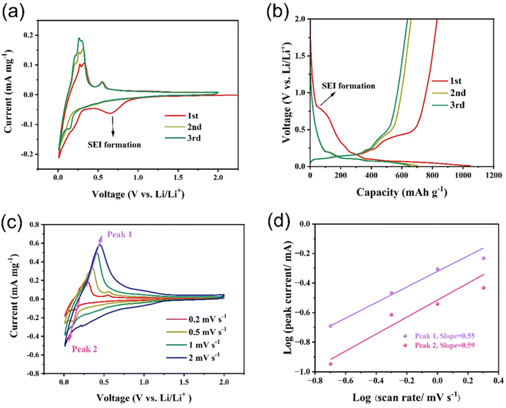 | ||
| Fig. 6 (a) Cyclic voltammetry (CV) curves at a scanning rate of 0.2 mV s−1 and (b) galvanostatic charge–discharge curves of Si/Ge/graphite@C, (c) CV curves of Si/Ge/graphite@C at various sweep rates, (d) linear relationship between logi (peak current) vs. logv (scan rate). | ||
4. Conclusions
In summary, the Si/Ge/graphite@C composite has been successfully synthesized by a ball-milling process followed by annealing in Ar/H2. The Si/Ge/graphite@C composite exhibits superior comprehensive properties relative to control groups. The excellent electrical conductivity and fast Li+ diffusivity of metal Ge enhance the electrochemical properties of the composite. Meanwhile, adding graphite can promote the tap density and capacity retention remarkably. In addition, the N-doped carbon coating layer from gelatin can improve the conductivity and the stability of interface during the charge/discharge process. Based on the synergistic effect of above advantages, the Si/Ge/graphite@C composite exhibits a high reversible capacity of 474 mA h g−1 with the ICE of 79.3%. This design and manufacturing strategy provides a reference for the practical application of silicon materials in the future.Author contributions
Ling Chang: conceptualization, methodology, validation, formal analysis, resources, writing – original draft preparation, supervision, project administration, funding acquisition. Yan Lin: software, validation, funding acquisition. Kai Wang: conceptualization, validation, investigation, writing – review and editing, project administration. Ruiqiang Yan: validation, formal analysis. Wei Chen: validation, investigation. Zecong Zhao: validation, resources. Yanping Yang: validation, data curation. Guobo Huang: methodology, validation, visualization, funding acquisition. Wei Chen: validation, resources. Jian Huang: validation, resources. Youzhi Song: validation, writing – review and editing, project administration.Conflicts of interest
There are no conflicts to declare.Acknowledgements
This research was funded by the Natural Science Foundation of Zhejiang Province (LQ20B030009), Zhejiang Province Public Welfare Technology Application Research Project (LGG22E010003), Science and Technology Project of Taizhou City (2003gy11), the Key Research and Development Projects of Zhejiang Province (2020C04004, 2021C03007), the Project for Science and Technology Innovation Leading Talents of Zhejiang Provincial High-level Talents Special Support Plan (2021R52028).References
- Z. T. Hu, W. H. Xing, S. Y. Gong, T. L. Sun, C. Wang, M. Hu, J. Zhao, Z. Y. Pan, W. Chen, Z. Chen and X. Y. Li, Colloids Surf., A, 2022, 643, 128779 CrossRef CAS.
- C. Y. Pei, T. Li, M. Zhang, J. W. Wang, L. Chang, X. Q. Xiong, W. Chen, G. B. Huang and D. M. Han, Sep. Purif. Technol., 2022, 290, 120875 CrossRef CAS.
- Z. J. Song, S. L. Fang, P. Xie, A. G. Zhong, C. X. Ma and D. M. Han, Appl. Surf. Sci., 2021, 540, 148365 CrossRef CAS.
- Z. J. Song, X. J. Shao, Q. Wang, C. X. Ma, K. D. Wang and D. M. Han, Int. J. Hydrogen Energy, 2020, 45, 2975–2988 CrossRef CAS.
- Y. Lin, J. B. Wu, X. H. Huang, G. X. Pan and X. H. Xia, J. Energy Chem., 2020, 51, 372–377 CrossRef.
- K. Wang, S. E. Pei, Z. S. He, L. A. Huang, S. S. Zhu, J. F. Guo, H. B. Shao and J. M. Wang, Chem. Eng. J., 2019, 356, 272–281 CrossRef CAS.
- M. T. McDowell, S. W. Lee, W. D. Nix and Y. Cui, Adv. Mater., 2013, 25, 4966–4985 CrossRef CAS PubMed.
- P. Li, H. Kim, S. T. Myung and Y. K. Sun, Energy Storage Mater., 2021, 35, 550–576 CrossRef.
- I. H. Son, J. H. Park, S. Kwon, S. Park, M. H. Rümmeli, A. Bachmatiuk, H. J. Song, J. Ku, J. W. Choi, J. M. Choi, S. G. Doo and H. Chang, Nat. Commun., 2015, 6, 7393 CrossRef CAS PubMed.
- Y. C. Zhang, Y. You, S. Xin, Y. X. Yin, J. Zhang, P. Wang, X. S. Zheng, F. F. Cao and Y. G. Guo, Nano Energy, 2016, 25, 120–127 CrossRef CAS.
- X. Y. Zhao and V. P. Lehto, Nanotechnology, 2020, 32, 042002 CrossRef PubMed.
- B. Philippe, R. Dedryvère, J. Allouche, F. Lindgren, M. Gorgoi, H. Rensmo, D. Gonbeau and K. Edström, Chem. Mater., 2012, 24, 1107–1115 CrossRef CAS.
- M. Y. Ge, J. P. Rong, X. Fang and C. W. Zhou, Nano Lett., 2012, 12, 2318–2323 CrossRef CAS PubMed.
- H. Wu, G. Chan, J. W. Choi, I. Ryu, Y. Yao, M. T. McDowell, S. W. Lee, A. Jackson, Y. Yang, L. B. Hu and Y. Cui, Nat. Nanotechnol., 2012, 7, 310–315 CrossRef CAS PubMed.
- H. Tian, H. J. Tian, W. Yang, F. Zhang, W. Yang, Q. B. Zhang, Y. Wang, J. Liu, S. R. P. Silva, H. Liu and G. X. Wang, Adv. Funct. Mater., 2021, 31, 2101796 CrossRef CAS.
- D. Y. Chen, X. Mei, G. Ji, M. H. Lu, J. P. Xie, J. M. Lu and J. Y. Lee, Angew. Chem., Int. Ed., 2012, 51, 2409–2413 CrossRef CAS PubMed.
- Y. L. An, H. F. Fei, G. F. Zeng, L. J. Ci, S. L. Xiong, J. K. Feng and Y. T. Qian, ACS Nano, 2018, 12, 4993–5002 CrossRef CAS PubMed.
- Z. Bitew, M. Tesemma, Y. Beyene and M. Amare, Sustainable Energy Fuels, 2022, 6, 1014–1050 RSC.
- H. M. Li, X. L. Li, D. H. Wang, S. Y. Zhang, W. Q. Xu, L. N. Zhu and L. J. Zhi, Nanoscale, 2021, 13, 2820–2824 RSC.
- L. J. Yan, H. W. Zhang, Z. H. Li, X. H. Gao, H. B. Wang, Z. Lin, M. Ling and C. D. Liang, ACS Appl. Energy Mater., 2020, 3, 10255–10260 CrossRef CAS.
- M. Y. Han, L. N. Zhao and J. Sun, Chem. J. Chin. Univ., 2021, 42, 3547–3560 Search PubMed.
- B. Liang, Y. P. Liu and Y. H. Xu, J. Power Sources, 2014, 267, 469–490 CrossRef CAS.
- F. C. Lyu, Z. F. Sun, B. Nan, S. C. Yu, L. J. Cao, M. Y. Yang, M. C. Li, W. X. Wang, S. F. Wu, S. S. Zeng, H. T. Liu and Z. G. Lu, ACS Appl. Mater. Interfaces, 2017, 9, 10699–10707 CrossRef CAS PubMed.
- J. K. Wu, F. Ma, X. R. Liu, X. Y. Fan, L. Shen, Z. H. Wu, X. Y. Ding, X. P. Han, Y. D. Deng, W. B. Hu and C. Zhong, Small Methods, 2019, 3, 1900158 CrossRef CAS.
- S. Chae, S. H. Choi, N. Kim, J. Sung and J. Cho, Angew. Chem., Int. Ed., 2020, 59, 110–135 CrossRef CAS PubMed.
- H. D. Chen, S. F. Wang, X. J. Liu, X. H. Hou, F. M. Chen, H. Pan, H. Q. Qin, K. H. Lam, Y. C. Xia and G. F. Zhou, Electrochim. Acta, 2018, 288, 134–143 CrossRef CAS.
- M. H. Parekh, V. P. Parikh, P. J. Kim, S. Misra, Z. M. Qi, H. Y. Wang and V. G. Pol, Carbon, 2019, 148, 36–43 CrossRef CAS.
- N. Lin, L. B. Wang, J. B. Zhou, J. Zhou, Y. Han, Y. C. Zhu, Y. T. Qian and C. H. Cao, J. Mater. Chem. A, 2015, 3, 11199–11202 RSC.
- A. Desrues, J. P. Alper, F. Boismain, D. Z. Dominguez, C. Berhaut, P. E. Coulon, A. Soloy, F. Grisch, S. Tardif, S. Pouget, S. Lyonnard and C. Haon, Batteries Supercaps, 2019, 2, 1–10 CrossRef.
- J. Q. Yin, Z. Y. Xu, Z. W. Xiao, H. B. Shao and J. M. Wang, J. Alloys Compd., 2022, 900, 163438 CrossRef CAS.
- I. Profatilova, E. D. Vito, S. Genies, C. Vincens and W. Porcher, ACS Appl. Energy Mater., 2020, 3, 11873–11885 CrossRef CAS.
- P. Li, J. Y. Hwang and Y. K. Sun, ACS Nano, 2019, 13, 2624–2633 CAS.
- H. M. Chen, Y. X. Zheng, Q. M. Wu, W. B. Zhou, Q. H. Wei and M. D. Wei, Electrochim. Acta, 2022, 417, 140337 CrossRef CAS.
- J. Lai, H. J. Guo, X. Q. Li, Z. X. Wang, X. H. Li, X. P. Zhang, S. L. Huang and L. Gan, Trans. Nonferrous Met. Soc. China, 2013, 23, 1413–1420 CrossRef CAS.
- W. Luo, D. K. Shen, R. Y. Zhang, B. W. Zhang, Y. X. Wang, S. X. Dou, H. K. Liu and J. P. Yang, Adv. Funct. Mater., 2016, 26, 7800–7806 CrossRef CAS.
- M. Cabello, E. Gucciardi, A. Herrán, D. Carriazo, A. Villaverde and T. Rojo, Molecules, 2020, 25, 2494 CrossRef CAS PubMed.
- K. Ma and N. Lin, Inorg. Chem. Front., 2019, 6, 1897–1903 RSC.
- Z. Liu, A. Borodin, X. X. Liu, Y. Li and F. Endres, J. Phys. Chem. C, 2021, 125, 13501–13507 CrossRef CAS.
- Y. G. Zhang, N. Du, C. M. Xiao, S. L. Wu, Y. F. Chen, Y. F. Lin, J. W. Jiang, Y. H. He and D. R. Yang, RSC Adv., 2017, 7, 33837–33842 RSC.
- Z. G. Mou, X. Y. Chen, Y. K. Du, X. M. Wang, P. Yang and S. D. Wang, Appl. Surf. Sci., 2011, 258, 1704–1710 CrossRef CAS.
- J. X. Wu, A. W. Tang, S. P. Huang, J. M. Li, L. X. Zeng and M. D. Wei, ACS Appl. Mater. Interfaces, 2020, 12, 46247–46253 CrossRef CAS PubMed.
- B. Zhu, G. L. Liu, G. X. Lv, Y. Mu, Y. L. Zhao, Y. X. Wang, X. Q. Li, P. C. Yao, Y. Deng, Y. Cui and J. Zhu, Sci. Adv., 2019, 5, 0651 Search PubMed.
- L. Chang, K. Wang, L. A. Huang, Z. S. He, S. S. Zhu, M. M. Chen, H. B. Shao and J. M. Wang, J. Mater. Chem. A, 2017, 5, 20892–20902 RSC.
- K. Wang, M. M. Chen, Z. S. He, L. A. Huang, S. S. Zhu, S. E. Pei, J. F. Guo, H. B. Shao and J. M. Wang, J. Alloys Compd., 2018, 755, 154–162 CrossRef CAS.
- B. B. Liu, A. R. Chen, R. F. Wang, T. Sun, J. Zhang, Y. Shu, J. Yang, C. Wang and Y. Yang, J. Inorg. Organomet. Polym., 2020, 30, 427–437 CrossRef CAS.
- H. S. Ji, J. Li, S. Li, Y. X. Cui, Z. J. Liu, M. G. Huang, C. Xu, G. C. Li, Y. Zhao and H. M. Li, J. Nanomater., 2022, 12, 2875 CrossRef CAS PubMed.
- Y. W. Lee, D. M. Kim, S. J. Kim, M. C. Kim, H. S. Choe, K. H. Lee, J. I. Sohn, S. N. Cha, J. M. Kim and K. W. Park, ACS Appl. Mater. Interfaces, 2016, 8, 7022–7029 CrossRef CAS PubMed.
- Z. S. He, L. A. Huang, J. F. Guo, S. E. Pei, H. B. Shao and J. M. Wang, Energy Storage Mater., 2020, 24, 362–372 CrossRef.
- Y. Z. Liu, Q. Deng, Y. P. Li, Y. J. Li, W. T. Zhong, J. H. Hu, X. H. Ji, C. H. Yang, Z. Lin and K. V. Huang, ACS Nano, 2021, 15, 1121–1132 CrossRef CAS PubMed.
Footnote |
| † Electronic supplementary information (ESI) available. See DOI: https://doi.org/10.1039/d2ra06311e |
| This journal is © The Royal Society of Chemistry 2023 |