
 Open Access Article
 This Open Access Article is licensed under a Creative Commons Attribution-Non Commercial 3.0 Unported Licence
Graphene oxide microstructure control of electrosprayed thin films†
Anton Karlsson *a,
Helena Grennbergb and
Stefan Johanssona
*a,
Helena Grennbergb and
Stefan Johanssona
aMicrosystems Technology, Department of Materials Science and Engineering, Uppsala University, Uppsala, Sweden. E-mail: anton.karlsson@angstrom.uu.se
bOrganic Chemistry, Department of Chemistry – BMC, Uppsala University, Uppsala, Sweden
First published on 3rd January 2023
Abstract
The graphene oxide (GO) microstructure, in terms of flake distribution, folding, and crumpling, in thin films affects properties such as electrical conductivity and optical transparency after GO reduction. A thin film can be tailored to the user's application if the microstructure resulting from different deposition methods can be controlled. In this work, we compare the microstructures of GO coatings created through electrospray deposition (ESD) with random deposition processes. The comparisons include both MATLAB simulations and a dip coating process. The microstructure of ESD GO thin films can be altered by changing the distance between the nozzle and the substrate. We developed a semi-automatic image analysis script that analyzes scanning electron microscopy images to find effects of GO stacking or agglomeration, without the risk of human bias. A low nozzle to substrate distance creates structures of flat GO flakes, but solvent flooding the samples causes drying patterns. A high nozzle to substrate distance causes folding and crumpling of the GO flakes due to solvent evaporation, resulting in agglomerated GO on the substrate. For our ESD setup, a nozzle to substrate distance of 2–4 mm produced GO coatings with the lowest combined influence of drying effects and GO flake folding or crumpling.
Introduction
Graphene is a material of great interest in many engineering and scientific applications due to properties such as single atomic layer thickness, high conductivity and transparency. Still, graphene oxide (GO) is a good starting material for many applications since it is much easier to produce and handle when compared with graphene.1 This allows for larger scale production of GO containing products compared with using graphene. Monolayered GO flakes are stable, for instance, in water at a wide range of pH values making it easy to handle. The stability of these suspensions is predominantly related to the electrostatic repulsion from ionized carboxylic groups with adjacent phenolic and hydroxyl groups decorating the GO flakes.2 The size of GO sheets can range from at least smaller than 10 nm (ref. 3) to above 1 mm.4 GO typically has low electrical conductivity, but the conductivity can be substantially increased by reducing the GO, forming reduced GO.5 These conductive reduced GO films can retain a high optical transparency if the thickness is low.6 Transparent conductive materials can be useful in applications such as optoelectronics and solar cells.7 There are several methods of producing GO thin films for transparent conductors,7 and quantifiable analysis methods of the produced films would be a useful tool to optimize GO flake distribution.Highly transparent films of GO have been created through the Langmuir Blodgett (LB) method, and are conductive upon thermal reduction and chemical doping.8 In the LB method, the depositing material is transferred from the surface of a liquid while that surface is being compressed by movable barriers. The first layer of deposited GO through a well optimized LB method forms a flat, dense structure of GO flakes without much overlap.9 However, subsequent layers can form wrinkled sheets due to repulsion from the first layer of GO.9 The degrees of wrinkling and folding should be minimized to keep a smooth surface with high transparency.7
Dip deposition is a similar process to the LB method. Both methods form coatings by withdrawing a substrate from a bath containing the depositing material. For dip deposition, the depositing material is typically in the bulk of the liquid, not only at the liquid surface as in the case of Langmuir Blodgett deposition. Withdrawing a substrate from the dip deposition liquid leaves a thin suspension film on the surface.10 The liquid film contains the particles that are suspended in the bath and the particles coat the substrate surface as the liquid evaporates.11 Therefore, by withdrawing substrates from suspensions of GO, a coating of GO can be achieved. The thickness of the deposited material can be controlled by e.g., changing the concentration of the suspension, substrate extraction speed as well as repeating the dipping process through several cycles. Dip deposition has been used to produce GO films of thicknesses spanning from sparsely deposited individual flakes12 up to several micrometers thick.13
Drop casting is done by dropping suspension onto a substrate and letting it dry. Drop casting is a fast and simple coating method but will likely form significant drying effects of “coffee-stain” patterns or wrinkling in the GO coating.14 Spin coating rotates the substrate as a suspension is dropped on it. The rotation spreads the suspension on the substrate to form a coating. However, the variation in GO coating thickness can be high in spin coated samples.7
Electrospray deposition (ESD) utilizes aerosolization of a suspension by electrical means. By applying a high voltage between a nozzle and substrate the liquid ejected from the nozzle forms an aerosol, travels to the substrate and forms a coating on the surface. ESD has been used as a method to produce GO coatings.15 The formed aerosol droplet size is somewhat controllable through applied voltage and liquid flow rate.16 The droplet size will also decrease due to evaporation as the droplets travels through the air.16 GO sheets will undergo crumpling during ESD as the liquid carrier droplets evaporate,17,18 which decreases coverage and optical transparency.7
The possibility of finding coating methods that are quick and can be repeated layer-by-layer to produce even coatings of certain microstructures is the basis to the following work in this article. These coatings could be used for thin film conductors after the subsequent reduction of the GO. The films can also be optically transparent if thin enough. It is crucial to investigate and develop a controllable process of not only deposition but also analysis methods. Ellipsometric contrast micrography has previously been used for quality control of chemical vapor deposited graphene on a large lateral scale by measuring the layer counts of graphene.19 For our samples, light optical microscopy (LOM) is used to characterize the coatings on a larger scale to visualize coating homogeneity while individual SEM micrographs are used to investigate deposition behavior and for microstructure elucidations. However, it can be difficult to determine and quantify the placement of GO flakes from scanning electron microscopy (SEM) images without tools to objectively measure the distribution. Therefore, we have developed a semi-automated analysis technique based on SEM images to quantifiably compare thin GO coatings with minimal risk of human bias. We have also made MATLAB simulations of randomly placed “GO flakes” to determine a baseline for how a random GO flake coating distribution would look like. Similar simulations have been performed previously for inkjet-printed GO dots,20,21 but, to the best of our knowledge, methods for quantifying arbitrary GO thin films of few layers with a sub-μm lateral resolution has not been available until the work presented here. In this work we analyze the similarities between dip coating, ESD coating, and simulated randomized coatings.
Results and discussion
Initial screening of coating methods
We selected drop casting, ESD, and dip coating as the potential quick and simple methods of forming GO thin film coatings on flat substrates. An initial screening study of these methods on substrates of Si with 285 nm thermally grown SiO2 demonstrates coating thickness through a color contrast.22 The dip coated sample in Fig. 1d has a relatively thick coating as seen by the overall color contrast, but the thickness is controllable, and suspensions of lower concentrations are used beyond the initial screening. The GO coating thickness of the ESD sample in Fig. 1c is low, the thickness is increased in the ESD samples of the main study by electrospraying lines with 50 μm separation instead of 200 μm as is the case here. The drop cast coating in Fig. 1a and b demonstrates a coating with a noticeable uneven surface. The center of the droplet (left of Fig. 1a) has a largely uncoated surface. The outer edge of the droplet (Fig. 1b) has rings of varying thicknesses. Drop casting as a method is excluded from the main study because of the inhomogeneous thickness it produces. | ||
| Fig. 1 LOM screening of GO suspension deposition methods on Si/SiO2 substrates, giving color contrast in LOM. Drop casting produces ring shapes with different thickness variation patterns in the center (a) and edge (b). ESD (c) and dip deposition (d) here produce coatings of different thicknesses, but can be adjusted by changing deposition parameters. Both ESD and dip coating have produced coatings without obvious thickness variations. | ||
Developing image analysis to measure surface coverage and microstructure
A semi-automatic image analysis MATLAB script is used to compare data over several images and samples without much human input. The image analysis of the SEM images is based on the pixel brightness getting lower (darker) for higher counts of GO layers overlapping. This can be seen in the example SEM image of a dip coated sample in Fig. 2a. The GO flakes range from sub-μm up to approximately 10 μm, and form areas of darker pixel brightness compared with the bare substrate background. From the SEM imaging brightness histogram Fig. 2b, we can see that there are peaks that correspond to the number of layers in the GO coating after pre-processing through median filtering. The peaks have different center points and peak shapes between histograms based on different images, possibly caused by surface charging, material loading, or if the SEM settings are changed. The image analysis script functions for different histograms as long as the peaks can be found. This means that we do not have to change the SEM settings during imaging or spend time with post processing. A minor manual adjustment of the parameters for the MATLAB function findpeaks() to detect the same number of peaks were made when needed. We can normally identify separate peaks for bare substrate, mono- and bi-layers thick GO-coating. Anything thicker than 2 layers are typically combined into one overlapping peak. The red vertical lines in Fig. 2b are the separating points between the peaks determined by the image analysis script. These points are automatically determined by finding the least pixel count between found peaks, and are used to annotate the separation between GO layer counts. The pixels between these separation points are shown in Fig. 2c, with color coding to show the determined layer count. The fraction of pixels with each annotation is then given as fraction of the imaged area. Peak deconvolution and peak height were also tested to determine the area fractions of the layer counts, but inconsistent peak shapes in the histogram caused us to use the separating points described earlier. | ||
| Fig. 2 Segmentation process of SEM images through pixel brightness. The SEM image of a GO dip coating on Si/SiO2 substrate (a) produces a histogram in (b). The histogram has peaks of pixel brightness which correspond to the increasing count of GO layers overlapping on the substrate. The red vertical lines in (b) denote the determined separation between GO layers and are used to segment the SEM image into the color-coded image (c) according to the determined area type, where dark blue is bare substrate, light blue is monolayered GO, yellow is bilayered GO, and red is 3+ layered GO. | ||
The GO layer counts given by the SEM image analysis are compared with non-contact atomic force microscopy (AFM) measurements of the same areas. This gives us the opportunity to see what the contrast in SEM means in layer height in the AFM. Fig. 3a and c are the raw images in SEM and AFM, respectively. Fig. 3b is the segmented result of the image analysis MATLAB script that illustrates the determined GO layer count using color coding. Fig. 3d is a cropped image from Fig. 3c, and contains the height measurements along the red line. A monolayer of this GO has a height of approximately 1.5 nm above the SiO2 surface of the substrate. A second layer of GO has a height of approximately 0.9 nm above the first layer. This non-linear height increase measured in AFM has been reported earlier for GO depositions on SiO2 substrates.23,24 Fig. 3 clearly show that the SEM image analysis method provides highly reliable data on GO layer count. Identified differences are typically seen at pixel level, i.e. very minor.
 | ||
| Fig. 3 Same area of an ESD sample showing the same GO flake using different views. (a) SEM image. (b) Segmented SEM image using our image analysis script. (c) Non-contact AFM image of the same area of ESD sample showing the measured topography. (d) Height measurements of GO flakes. The red line is the measurement path shown in the white height measurements. | ||
Image analysis giving layer counts is not in itself sufficient to tell if GO flakes are not affecting each other, leading to a random distribution, or if there are phenomena of increasing or decreasing GO agglomeration, monolayer proportion, flake folding, etc. What would a random coating look like and how do we measure it? We performed MATLAB simulations of “GO flakes” randomly thrown out on a virtual surface without flake folding. These simulated flakes have a square to rhombus shape and a size distribution visually similar to the GO flakes in the ESD ink. In accordance with literature,20,21 we found the simulated coating surface coverage to follow a Poisson distribution. Fig. 4 shows the average area fractions of the GO layer counts determined using the image analysis on dip coated samples. The results are presented as percentages of bare substrate up to 3+ GO layer count on the substrate. A Poisson distribution is fitted to the experimental data using least squares regression, and it corresponds very well to the MATLAB simulated coating, indicating that GO formed a random coating on the dip deposited samples. This also indicates a low influence from an inter-flake and substrate–flake interaction phenomena in the deposition of individual GO flakes. The simulations will hence provide a baseline for comparisons with the ESD results below.
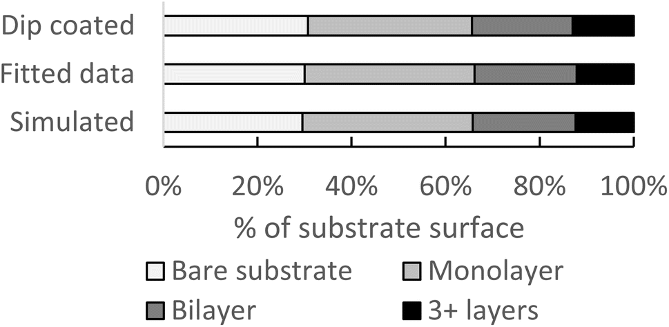 | ||
| Fig. 4 Area fractions of the segmented SEM images of dip coated samples. Fitted data is a Poisson distribution applied to the dip coated results using least-squares regression. Simulated results are randomly placed “GO flakes” over a simulated area. Simulated flakes are placed until an average layer count determined in accordance with the Poisson fit is reached. | ||
ESD nozzle to substrate distance series in comparison to dip deposition
In the initial screening (Fig. 1), it was found that the deposition of GO by ESD has a different outcome than dip deposition. Moreover, in particular, the nozzle to substrate distance had a profound influence on the outcome on surface coverage, layer count, and microstructure. The fraction of coated surface decreases with increasing nozzle to substrate distance even though equal amounts of suspension are deposited over the same area.LOM imaging of ESD samples with a 2 and 4 mm nozzle to substrate distance in Fig. 5 visually appears similar to the dip coated sample. The ESD samples with 1, 8, and 12 mm distance are visually different from the dip coated image. There are patterns similar to coffee-staining in the ESD sample with 1 mm distance. These patterns show areas of both bare substrate with no GO coating, and areas of higher layer counts. The patterns are likely caused by solvent flooding the sample as this was observed during the ESD process. A grainy surface texture can be seen at high ESD nozzle to substrate distances of 8 and 12 mm, which indicates agglomeration of the GO flakes.
 | ||
| Fig. 5 LOM imaging of GO deposited on SiO2 wafer using (a) dip deposition, (b–f) ESD with different nozzle to substrate distances: (b) 1, (c) 2, (d) 4, (e) 8, (f) 12 mm. Samples prepared from suspensions containing 0.12 mg mL−1 GO in (a) 30 vol% water – 70 vol% isopropyl alcohol, (b–f) 3 vol% water – 97 vol% ethanol. | ||
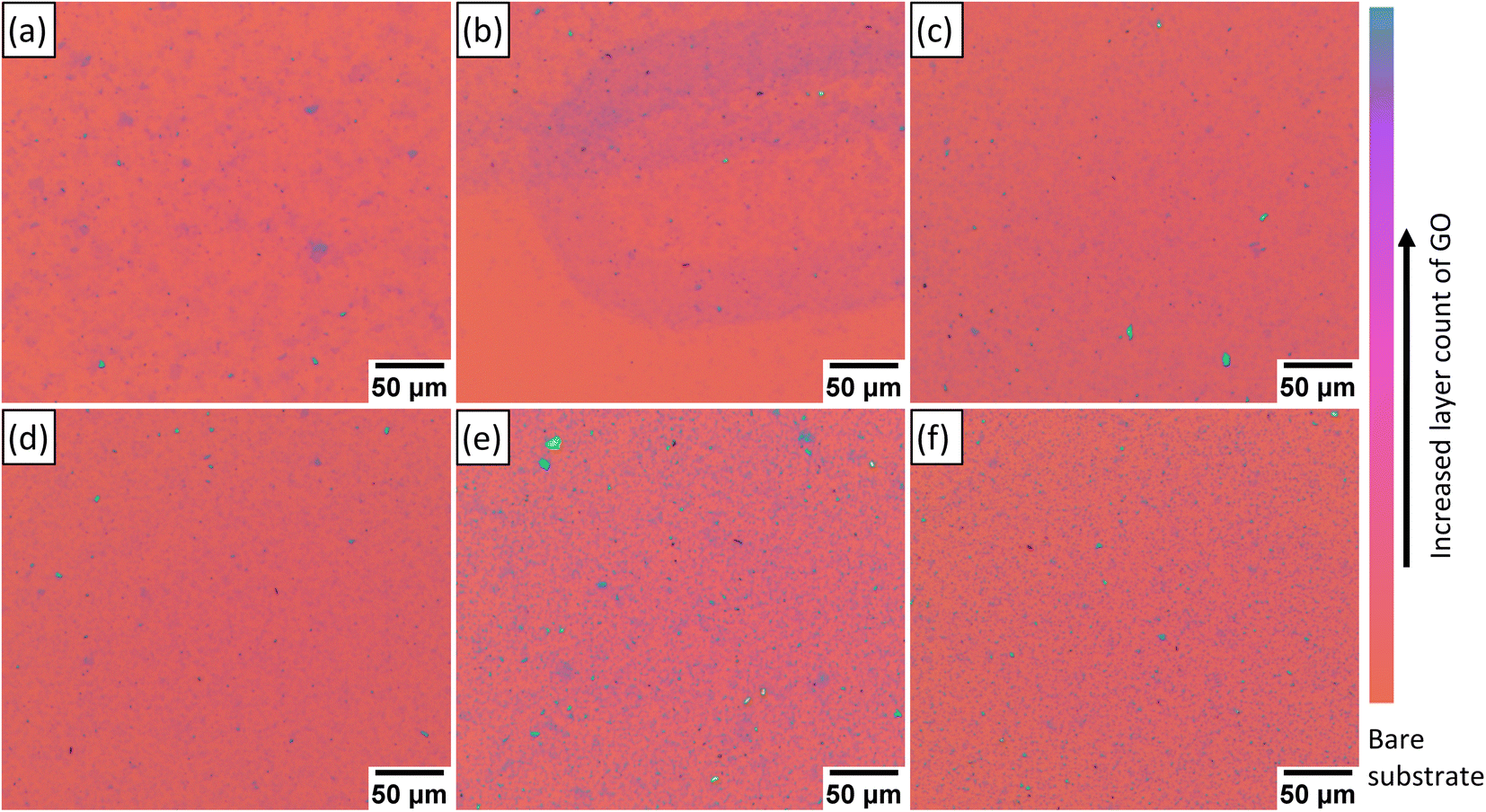
The microstructure of the ESD samples is continually changing throughout an increasing nozzle to substrate distance in Fig. 6. The GO flakes are seen deposited in a flat manner at the closest distance of 1 mm. However, there are also clusters of agglomerated GO flakes, possibly similar to the coffee-stain appearance. At increased ESD nozzle to substrate distances, there is an increase of agglomeration or folding of the GO flakes. This can be clearly seen at nozzle to substrate distances of 8 and 12 mm (Fig. 6e and f) where most of the GO consists of higher number of stacked GO layers. These areas are seen as separated islands of thicker coating, with the immediate large change in contrast. The SEM images of ESD samples at all nozzle to substrate distances are not visually similar to simulated coatings (ESI, Fig. S8†) due to the folded, crumpled, and agglomerated GO flakes.
 | ||
| Fig. 6 (a) SEM image of dip coated sample. (b–f) SEM images of ESD with different nozzle to substrate distances: (b) 1, (c) 2, (d) 4, (e) 8, (f) 12 mm. Samples prepared from suspensions containing 0.12 mg mL−1 GO in (a) 30 vol% water – 70 vol% isopropyl alcohol, (b–f) 3 vol% water – 95 vol% ethanol. | ||
The dip coated sample shows flat flakes of a larger size than the ESD samples. Exposure to ultrasonic baths breaks the GO flakes and decreases their size.25 The different ink recipes for dip coating and ESD may result in different GO flake size distributions. Larger GO flakes should not affect the average distribution of area fractions of bare substrate or the different number of GO layers if the deposition follows a random distribution, but it should increase the variance of the measurements.21
The image analysis method is used on the ESD nozzle to substrate test series to provide a comparison technique without human bias. We compare the image analysis results of different ESD nozzle to substrate distances and the results from the MATLAB simulations of a similar coating thickness in Fig. 7. The results are shown as surface coverage in (a) and layer count distribution within coated areas in (b). The fraction of bare substrate is increased with increasing nozzle to substrate distance, even though equal volumes of suspension is electrosprayed in an equidistant pattern for all samples and the large coated area should remove any boundary effects. Both the 1 mm and 8 mm nozzle to substrate distance samples have the majority of GO as 3 layers or more, while the intermediate distances have more than 50% mono- or bilayered GO. MATLAB simulation results with a similar average layer count as the ESD samples with a nozzle to substrate distance of 2 and 4 mm are included to show the area fractions of a coating with no GO flake folding, crumpling, or agglomeration.
 | ||
| Fig. 7 SEM image analysis results of ESD samples with an increasing nozzle to substrate distance. Bottom row is MATLAB simulation results. (a) Area fraction of bare substrate with no GO coating. (b) Layer count distribution within the GO coated area. | ||
To evaluate if ESD leads to a random distribution of GO flakes, the goodness of the fit to a random distribution of the ESD samples are shown in Fig. 8a. The residuals in the figure are the average difference between experimental values and the fitted Poisson distributions. All ESD coated samples have higher residuals compared with the dip coated samples, but the samples with a nozzle to substrate distance of 8 mm stand out with the highest residuals. This poor fit is caused by the high area fractions of both bare substrate and 3+ layers of GO seen in Fig. 7. We can see that the lowest average residual for the ESD samples is obtained at a nozzle to substrate distance of 2 mm. While a nozzle to substrate distance of 2 mm in our present ESD setup forms coatings that most closely fits a random distribution, the optimal distance would likely depend on different ESD parameters used. For example, adjusting the applied voltage or suspension flow rate would change the size of the droplets formed16 which could affect the optimal ESD nozzle to substrate distance.
 | ||
| Fig. 8 (a) Mean value of the residuals between measured data and best fitting Poisson distribution though least-squares regression. The percentages are percentage points of area fractions in Fig. 4 and 7. Error bars show the 95% confidence interval of the mean. Individual measurements and fitted data are given in ESI material Fig. S10.† (b) Pooled ± 1-σ standard deviation for each sample type. The standard deviation is primarily a measurement of coating consistency over several images and samples, where lower is more consistent. | ||
The standard deviation between individual images is a measure of coating homogeneity (Fig. 8b). A GO coating that is homogenous over a large area would give image analysis results with a low deviation over the different images in the series, similar to the MATLAB simulated results. For this measurement, the ESD samples with a nozzle to substrate distance of 1 mm stands out with the highest standard deviation. This is caused by the staining patterns seen in the LOM imaging (Fig. 5b), so the thickness variation is also apparent in the SEM image series. ESD samples deposited at a 2 mm nozzle to substrate distance have a smaller increase in standard deviation, which suggests the presence of a similar, albeit lesser, effect to that at 1 mm.
A model for the microstructure formation process
The results of ESD thin films deposited at different nozzle to substrate distances shown in the LOM and SEM imaging can be combined to suggest an explanation of the deposition behavior. Fig. 9 shows a schematic image of the suggested effects of increasing the nozzle to substrate distance. Included in the figure are the droplets in-flight, droplets on the substrate, and deposited GO on the substrate. We know from literature17,18 that GO flakes crumple within an electrosprayed droplet due to solvent evaporation. If we have a short nozzle to substrate distance (Fig. 9a), the droplets are relatively large as not much solvent has evaporated. The GO flakes are well dispersed and flat, but the excessive solvent floods the substrate, possibly causing coffee stain effects. Also, the closer nozzle to substrate distance causes the spread of the electrospray to be decreased,26 and we observed the electrospray to be unstable at 1 mm. Both of these effects are contributing factors to the suspension flooding of the samples causing risk of coffee-stain type patterns. At medium nozzle to substrate distance, here approximately 2–4 mm in Fig. 9b, the droplets are smaller due to solvent evaporation. This causes a small amount of crumpling and folding of the GO flakes. Smaller droplets and a larger electrospraying spread decreases substrate flooding, and the drying effects on the substrate are removed. The resulting GO coating will have some crumpled and folded GO flakes, but the lowest residual between experimental data and a Poisson fit is seen at 2 mm (Fig. 8a). This is likely a result of a minimum trade-off point between the phenomena of coffee-staining effects for short nozzle to substrate distances and flake agglomeration, as both of these phenomena will increase the area fractions of 3+ layers of GO and bare substrate. The solvent evaporation causes the droplets to shrink further at the highest nozzle to substrate distances (Fig. 9c). The GO is agglomerated and is deposited in smaller areas with high layer counts as seen in Fig. 6e and f. | ||
| Fig. 9 Schematic image showing the in-flight- and on substrate agglomeration effects on the suspended GO depending on the nozzle to substrate distance during ESD. (a) A very short nozzle to substrate distance contains relatively large droplets that flood the substrate, depositing flat flakes but causes drying effects on the substrate. (b) The droplets shrink from solvent evaporation at a medium nozzle to substrate distance (db < da). This causes the GO flakes to start folding and crumpling in-flight. (c) At very large nozzle to substrate distances the droplets shrink further (dc < db) and the GO flakes agglomerate in the small droplets already before reaching the substrate. | ||
The phenomena occurring when using very short or long nozzle to substrate distances may be addressed to widen the range of viable nozzle to substrate distance for a desired microstructure. A heated substrate could be added to the ESD setup to decrease the thickness variation27 that cause the patterns similar to coffee-staining of ESD with 1 mm of nozzle to substrate distance. Different evaporation rates of the solvents used will lead to different times until aggregations form within the ESD aerosol droplets.28 Increasing droplet size or decreasing the evaporation rate may decrease agglomeration at large distances between the nozzle and substrate.
Conclusions
LOM and SEM are useful characterization methods when investigating the quality of coatings of GO flakes. Our image analysis MATLAB script allowed us to quantitively describe the distribution of layers of GO flakes from SEM images using pixel brightness. We have used this image analysis tool to compare dip coating with ESD of GO flakes on these samples. This work allows users to further optimize ESD of GO flakes or other methods of deposition in future work.Simulations done in MATLAB have validated that randomly distributed GO flakes will form coatings with overlapping layers counts closely following a Poisson distribution. Therefore, the results from the image analysis of SEM images can be compared with Poisson distributions to measure how close to random distributions the experimental setups produce.
Dip deposition of GO suspension on Si/SiO2 substrates have been created as comparison references to ESD coated substrates, which this work is focused on. The dip coated samples show coatings of GO flakes deposited flatly. Image analysis of these samples show that the distribution closely follows a Poisson fit, therefore the deposition of GO flakes through dip deposition follows a randomized process. ESD has shown effects that causes the deposited coatings to deviate from a randomized coating. A short distance between the ESD nozzle and substrate surface gives a coating with flat, extended GO flakes, but have coffee-stain-like patterns and coating thickness variation on a larger scale. Opposite this, a large nozzle to substrate distance creates coatings with low thickness variation on larger scales, but the GO flakes are folded and crumpled which increases the area fractions of 3+ layers of GO and bare substrate. A high nozzle to substrate distance is useful if the aim is to distribute GO agglomerations on a substrate. If the aim is to create thin coatings of flat GO flakes with a high monolayered content, there is an optimal distance that minimizes the effect of the two phenomena of thickness variation and flake agglomeration. We found that our setup and conditions created coatings closest to a randomized distribution using for the nozzle to substrate distance of 2 mm. We expect that this result of ESD nozzle to substrate distance is dependent on other parameters used, such as type of solvent evaporation rate, liquid flow rate, and applied voltage.
Methods and materials
General
Concentrated GO suspension (4 mg mL−1 in water) was acquired from Graphenea, Spain. Isopropyl alcohol (Aldrich, electronic grade ≥99.5%), ethanol (VWR, ACS reagent grade ≥99.8%), and acetone (Sigma Aldrich, ACS reagent grade, ≥99.5%) were all used as received. All solvent bottles were only opened to transfer content to single use glass vials. Fresh deionized water was used from tap.Si wafer pieces with a 285 nm thick SiO2 layer (P-type doped, Graphene Supermarket, USA) were used as substrates. The wafers were cut with the polished side down against a cleanroom wipe (VWR 1000 series) into approximate 10 × 10 mm squares by hand using a glass cutting tool. Any pieces of wafer debris were removed with cleanroom wipes. The cut samples were stored individually in 3D printed sample wells. The substrates for ESD were rinsed using acetone and isopropyl alcohol 1 day prior to ESD. The cleaned substrates were let dry horizontally, polished side down against a cleanroom wipe. The cleaned substrates were then stored in a pre-chamber overnight in a humidified N2 gas flow of 2 to 5 L min−1 at a relative humidity set to 40% (Preservatech Mini One).
Motorized dip deposition
A 10 mL beaker was filled with a mixture from 0.3 mL (3 vol%) of as received GO suspension, 2.7 mL (27 vol%) of deionized water, and 7 mL (70 vol%) of isopropyl alcohol. Isopropyl alcohol was chosen for dip deposition as it did not show a strong “tears-of-wine” Marangoni effect when a substrate was extracted from the suspension. The suspension was sonicated for 15 minutes (Struers Metason 50) to re-disperse any sedimented and agglomerated flakes.29 The suspension was also stirred in the beaker to mix thoroughly shortly before the dip deposition. The dipping procedure was performed using a piezoelectric motor (PiezoMotor LTC2013 motor with a PMD101 controller). We developed a LABView program that automated the controller. The linear motor was connected to a rod that held the sample in a vertical position. As the sample was lowered into the suspension, no part of the rod or sample holder was in contact with the suspension. Therefore, a corner of wafer pieces was never dipped. The dipping speed was set to 2.2 mm s−1 and the raising speed was 22 μm s−1 ≈ 1.3 mm min−1. The dipping length was 11 mm and there was a 30 seconds stationary pause when the sample was submerged. 5 Wafer pieces in total were dipped subsequently, though one was discarded due to visible droplet formation on the surface. The ambient conditions were 21.5 degrees Celsius and 49.5% relative humidity.ESD series of nozzle to substrate distance
A suspension of 3 vol% as received GO suspension was diluted in 97 vol% ethanol resulting in a 0.12 mg mL−1 GO suspension. The ethanol is used to lower the surface tension of the suspension compared with only using water. The lower surface tension makes ESD viable. The suspension was sonicated for 30 minutes (VWR USC-TH). A glass high pressure syringe was filled with the suspension. The syringe was mounted in an in-house developed 3D printing setup. A linear motor (PiezoMotor LTC2013) acted as a syringe pump. The syringe had a stainless-steel needle with an outer diameter of 520 μm and internal diameter of 180 μm. The needle was connected to the positive output of a high voltage source (S3CP030) that can apply up to 3.0 kV. A conductive carbon adhesive tab was used as the sample holder, and was connected to the negative output of the high voltage source. In-house developed LabVIEW programs controlled the 3D printing setup with the syringe and syringe pump attached to the z-axis. A coordinate file was loaded into the program and acted as the printing pattern. The ESD was performed with the syringe mounted horizontally and with the substrate mounted perpendicular to the needle of the syringe. A stereo microscope with a camera was mounted above the ESD setup, and was used to confirm the formation of a Taylor cone. Parallel lines separated by 50 μm covering an 8 mm by 8 mm area were used in coating these samples. The printer followed this pattern at a speed of 8 mm s−1.The distance between the nozzle and substrate varied between 1 to 12 mm. The pump motor speed was set to 2 μm s−1, corresponding to 3.3 nL s−1 of suspension. The applied voltage between the needle and sample was nominally 3.0 kV, but decreased to 2.5 kV for a nozzle to substrate distance of 2 mm, and 1.7 kV for a distance of 1 mm. A higher applied voltage at those distances resulted in a corona discharge at the needle tip. A humidity controller (Preservatech Mini One) modified to humidify N2 gas was used to keep the relative humidity at 38 ± 4% at 22.5 ± 0.5 °C inside an ESD chamber containing the substrate and needle, as well as a sample storage box prior to the ESD. The N2 flow through the ESD chamber varied between approximately 2 to 5 L min−1 over the test series.
Pre-screening study
ESD pre-screening was done without humidity control, a nozzle to substrate distance of 4 mm, and with a printing pattern of 200 μm between parallel lines, otherwise following the ESD series described above. The dip coating pre-screening used a suspension of 25 vol% as received GO suspension diluted with 75 vol% water. The substrate was submerged for 300 s before withdrawal. The drop casting used an autopipette to deposit a 50 μL drop of the same suspension as the ESD series above directly on a horizontal Si/SiO2 substrate. The sample was left to dry in ambient conditions.Coating characterization
LOM of GO on substrates of Si/SiO2 substrates is a fast way of identifying single- to few-layer graphene materials.22 We used an Olympus BX60M microscope with a Toupcam camera to characterize the GO coated samples over a larger area than possible with the other characterization methods used here.The SEM images used in the image analysis were taken with a Zeiss LEO 1530 SEM with an inlens secondary electron detector. 9 images in a 3 by 3 grid were taken with 0.5 mm between each image on the samples. The images of ESD and dip coated samples used a magnification of 5 kx and 3 kx, respectively. The brightness and contrast were set to have a high brightness difference between the peaks of bare substrate and 3+ layers of GO.
The Image analysis script produced a brightness histogram for each individual SEM image. 4 peaks were separated in each histogram and correspond to bare substrate, monolayered GO, bilayered GO and 3+ layers of GO. These peaks were used to separate pixel brightness that correspond to the corresponding GO layer numbers. The images were then segmented using pixel brightness. Pixel count of each layer count gave us surface coverages in percent for each image. The average standard deviation for each area fraction of bare substrate up to 3+ layers of GO were used for Fig. 6b. The images were pre-processed prior to the image analysis with median filtering to decrease the effect of noise.
Atomic force microscopy (AFM) (PSIA/Park systems XE-150) in a non-contact configuration was used to investigate the SEM image analysis to give a sense of how well the SEM pixel brightness corresponded to the layer count of GO flakes.
Conflicts of interest
The authors declare no conflict of interest.Acknowledgements
We gratefully acknowledge the financial support from the Swedish Research Council (contract number 2018-04064). We acknowledge Myfab Uppsala for providing facilities and experimental support. Myfab is funded by the Swedish Research Council (2019-00207) as a national research infrastructure.References
- S. Gilje, S. Han, M. Wang, K. L. Wang and R. B. Kaner, A Chemical Route to Graphene for Device Applications, Nano Lett., 2007, 7(11), 3394–3398 CrossRef CAS PubMed.
- B. Konkena and S. Vasudevan, Understanding aqueous dispersibility of graphene oxide and reduced graphene oxide through pKa measurements, J. Phys. Chem. Lett., 2012, 3(7), 867–872 CrossRef CAS PubMed.
- D. Pan, J. Zhang, Z. Li and M. Wu, Hydrothermal Route for Cutting Graphene Sheets into Blue-Luminescent Graphene Quantum Dots, Adv. Mater., 2010, 22(6), 734–738 CrossRef CAS PubMed.
- C. Y. Su, Y. Xu, W. Zhang, J. Zhao, X. Tang and C. H. Tsai, et al., Electrical and spectroscopic characterizations of ultra-large reduced graphene oxide monolayers, Chem. Mater., 2009, 21(23), 5674–5680 CrossRef CAS.
- S. Stankovich, D. A. Dikin, R. D. Piner, K. A. Kohlhaas, A. Kleinhammes and Y. Jia, et al., Synthesis of graphene-based nanosheets via chemical reduction of exfoliated graphite oxide, Carbon, 2007, 45(7), 1558–1565 CrossRef CAS.
- H. A. Becerril, J. Mao, Z. Liu, R. M. Stoltenberg, Z. Bao and Y. Chen, Evaluation of solution-processed reduced graphene oxide films as transparent conductors, ACS Nano, 2008, 2(3), 463–470 CrossRef CAS PubMed.
- Q. Zheng and J. K. Kim, Graphene for Transparent Conductors, Graphene for Transparent Conductors, Springer, New York, 2015 Search PubMed.
- Q. Zheng, W. H. Ip, X. Lin, N. Yousefi, K. K. Yeung and Z. Li, et al., Transparent Conductive Films Consisting of Ultralarge Graphene Sheets Produced by Langmuir–Blodgett Assembly, ACS Nano, 2011, 5(7), 6039–6051 CrossRef CAS PubMed.
- L. J. Cote, F. Kim and J. Huang, Langmuir–Blodgett assembly of graphite oxide single layers, J. Am. Chem. Soc., 2009, 131(3), 1043–1049 CrossRef CAS PubMed.
- M. Maleki, M. Reyssat, F. Restagno, D. Quéré and C. Clanet, Landau–Levich menisci, J. Colloid Interface Sci., 2011, 354(1), 359–363 CrossRef CAS PubMed.
- A. Gans, E. Dressaire, B. Colnet, G. Saingier, M. Z. Bazant and A. Sauret, Dip-coating of suspensions, Soft Matter, 2019, 15(2), 252–261 RSC.
- X. Dong, C. Y. Su, W. Zhang, J. Zhao, Q. Ling and W. Huang, et al., Ultra-large single-layer graphene obtained from solution chemical reduction and its electrical properties, Phys. Chem. Chem. Phys., 2010, 12(9), 2164–2169 RSC.
- K. Bhowmik, S. Pramanik, S. K. Medda and G. De, Covalently functionalized reduced graphene oxide by organically modified silica: a facile synthesis of electrically conducting black coatings on glass, J. Mater. Chem., 2012, 22(47), 24690–24697 RSC.
- W. S. Chong, S. X. Gan, H. M. Al-Tuwirit, W. Y. Chong, C. S. Lim and H. Ahmad, Nanolitre solution drop-casting for selective area graphene oxide coating on planar surfaces, Mater. Chem. Phys., 2020, 249, 122970 CrossRef CAS.
- M. Mustafa, M. N. Awais, G. Pooniah, K. H. Choi, J. Ko and Y. H. Doh, Electrospray deposition of a graphene-oxide thin film, its characterization and investigation of its resistive switching performance, J. Korean Phys. Soc., 2012, 61(3), 470–475 CrossRef CAS.
- A. Jaworek, Electrospray droplet sources for thin film deposition, J. Mater. Sci., 2007, 42(1), 266–297 CrossRef CAS.
- S. Kavadiya, R. Raliya, M. Schrock and P. Biswas, Crumpling of graphene oxide through evaporative confinement in nanodroplets produced by electrohydrodynamic aerosolization, J. Nanopart. Res., 2017, 19(2), 43 CrossRef.
- H. Tang, C. Yang, Z. Lin, Q. Yang, F. Kang and C. P. Wong, Electrospray-deposition of graphene electrodes: a simple technique to build high-performance supercapacitors, Nanoscale, 2015, 7(20), 9133–9139 RSC.
- P. Braeuninger-Weimer, S. Funke, R. Wang, P. Thiesen, D. Tasche and W. Viöl, et al., Fast, noncontact, wafer-scale, atomic layer resolved imaging of two-dimensional materials by ellipsometric contrast micrography, ACS Nano, 2018, 12(8), 8555–8563 CrossRef CAS PubMed.
- J. Lee, C. Wang, S. Zhou and J. Chen, Spatial distribution quantification and control of ink flakes in reduced graphene oxide FET inkjet printing, In Elsevier B.V., 2019, pp. 19–25 Search PubMed.
- J. Lee, S. Zhou and J. Chen, Statistical Modeling and Analysis of k-Layer Coverage of Two-Dimensional Materials in Inkjet Printing Processes, Technometrics, 2020, 63(3), 410–420 CrossRef.
- P. Blake, E. W. Hill, A. H. Castro Neto, K. S. Novoselov, D. Jiang and R. Yang, et al., Making graphene visible, Appl. Phys. Lett., 2007, 91(6), 063124 CrossRef.
- I. Jung, M. Pelton, R. Piner, D. A. Dikin, S. Stankovich and S. Watcharotone, et al., Simple approach for high-contrast optical imaging and characterization of graphene-based sheets, Nano Lett., 2007, 7(12), 3569–3575 CrossRef CAS.
- K. A. Mkhoyan, A. W. Contryman, J. Silcox, D. A. Stewart, G. Eda and C. Mattevi, et al., Atomic and electronic structure of graphene-oxide, Nano Lett., 2009, 9(3), 1058–1063 CrossRef CAS PubMed.
- S. Ye and J. Feng, The effect of sonication treatment of graphene oxide on the mechanical properties of the assembled films, RSC Adv., 2016, 6(46), 39681–39687 RSC.
- O. Wilhelm, L. Mädler and S. E. Pratsinis, Electrospray evaporation and deposition, J. Aerosol Sci., 2003, 34(7), 815–836 CrossRef CAS.
- A. P. Taylor and L. F. Velásquez-García, Electrospray-printed nanostructured graphene oxide gas sensors, Nanotechnology, 2015, 26(50), 505301 CrossRef PubMed.
- V. B. Shah and P. Biswas, Aerosolized droplet mediated self-assembly of photosynthetic pigment analogues and deposition onto substrates, ACS Nano, 2014, 8(2), 1429–1438 CrossRef CAS PubMed.
- Graphene Oxide [Internet]. [cited 2022 Mar 11]. available from: https://www.graphenea.com/collections/graphene-oxide/products/graphene-oxide-4-mg-ml-water-dispersion-1000-ml.
Footnote |
| † Electronic supplementary information (ESI) available. See DOI: https://doi.org/10.1039/d2ra06278j |
| This journal is © The Royal Society of Chemistry 2023 |