
 Open Access Article
 This Open Access Article is licensed under a Creative Commons Attribution-Non Commercial 3.0 Unported Licence
Photoresponse of CVD grown crystalline quantum dot-embedded covalent organic framework thin film
Neha Chaki Roy *a and
Tapanendu Kundub
*a and
Tapanendu Kundub
aCentre for Research in Nanotechnology & Science (CRNTS), Indian Institute of Technology (IIT Bombay), India. E-mail: nihacroy@gmail.com
bDepartment of Physics, Indian Institute of Technology (IIT Bombay), India. E-mail: t.kundu@iitb.ac.in
First published on 25th January 2023
Abstract
Covalent organic frameworks (COFs) are a new family of novel 2D materials which are highly sought after for integration into future sensors and other devices for their highly porous structures and large surface areas. However, low-temperature large-area growth of these semiconductive materials with a clean surface for direct device applications is still a challenging task. To provide an on-chip photonic device, a COF366-Quantum dot (COF366-QDs) thin-film-based device fabricated by in situ chemical vapor deposition (CVD) is presented. The high-resolution transmission electron microscopy (HRTEM) displays the formation of the periodic, crystalline and porous framework of the COF layer with mono-dispersed QDs of average particle size of ∼2.5–3 nm. The fabricated COF366-QD layer acts as a photoactive layer in the photonic device with an Au-COFQD-Au structure where a conduction path is formed between the metal electrodes through a network of COF layer with embedded QDs. The device shows photoactive response under 514 nm visible light with a very low dark current of 4.36 × 10⁻¹¹ A with a minimum light detection capability of 160 nW and a responsivity of ∼3.42 A W−1. The photonic device was highly stable for successive switching cycles with very low attenuation. To our knowledge, this is the first report of a Quantum dot embedded COF366 thin-film by chemical vapor deposition. The proposed interfacing of COF366-QD thin-films on silicon substrate using in situ low-temperature CVD technique can be highly valuable for the development of transfer-free, clean, and low-cost preparation of industrial-scale organic electronics, optoelectronic device applications, and lab-on-chip based technologies for a wide range of future applications.
Introduction
Two-dimensional (2D) materials have revolutionized the semiconductor industry with their extraordinary electronic and optoelectronic properties in the last decade. This has opened new horizons for the exploration and innovation of new 2D materials. Covalent organic frameworks (COF) are novel smart materials with well-defined and adjustable porosity,1 large surface area, intrinsic crystalline framework, high thermal stabilities,2 conductive3/semiconductive properties, and ease of modifying the chemical structure, which has attracted intense attention in various applications ranging from gas adsorption/separation,4,5 energy storage,6,7 advanced sensing,8–13 semiconductive device,14–18 biological applications,19–22 photocatalysis23,24 etc. These materials have π-electronic blocks covalently bonded and arranged in periodic planar networks stacked in layered 2 or 3-dimensional (2D or 3D) network structures with atomic precision. The highly crystalline nature and π-stacking monomers of COF provide the passage for charge transport and thus the ability to tailor electronic transport in the stacked COF layers makes it capable of its unique electronic and optoelectronic properties for various applications.25–27 In recent years, remarkable efforts have been presented towards the deposition of well oriented and thickness semiconductive COF thin-films on flexible substrates and architectures for direct device applications.28–31Traditionally, solvothermal synthesis32–35 or adaptive methods have been used for the growth of semiconducting COF films for various device applications ranging from photonic sensors,36–38 photovoltaic devices,39 and electronic devices.40–42 The major hindrance in device fabrication is their non-solubility in the majority of the solvents, long reaction time, and most of the device applications would need COF as a thin-film and not as microcrystalline powder. The COF-based device fabrication would need control of their thickness, orientation, location, uniformity, and large-area growth on suitable substrates with a clean surface. However, the traditional techniques provide poorly controlled nucleation and aggregation and are quite difficult for integrating these COF-thin films with commercial microfabrication processes. Further, the porphyrin-based COF synthesis solution leads to chemical contamination making it difficult for microfabrication processing, and electrode fabrication and thus embedding them in various CMOS/MEMS,43,44 optical,45,46 sensor devices.47,48 Chemical Vapor Deposition (CVD) is a remarkable technology in the field of nanofabrication for uniform thin films with precise control of thickness and morphology.
In this respect, CVD technique is exemplary for transferring the intrinsic semiconducting properties of COF on large area wafer-scale preparation of direct devices. Lately, several attempts have been made to deposit COF thin-films using vapor-induced deposition,49 flow-cell configuration, and chemical vapor deposition.50–52 Remarkably, as a new development, Liu et al..recently reported a vapor-induced process for large-scale synthesis of 2D-COF films on several substrates.53 Another group reported COF-TpPa1 membranes fabrication by CVD method and used the membranes for dye separation.50 COF-366 is one of the pioneering and promising porphyrin based-COF with very high charge carrier mobility reported by Yaghi and co-workers and later several research groups presented applications of COF-366.54–58 However, chemically stable, crystalline, and large area-growth of porphyrin-containing COF-366 using chemical vapor deposition technique has not been explored much and therefore a modest attempt has been made here. Here, we present our tactically controlled fabrication of COF by imine condensation of 5,10,15,20-tetrakis(4-aminophenyl)porphyrin (TAPP) with 1,4-benzenedicarboxaldehyde (BDA) by chemical vapor deposition (CVD) to fabricate COF366-QD based photoactive device. A taxonomic study of the structural and morphological characteristics of the COF366-QD layer has been carried out. A methodical study of the opto-electrical characteristics of the devices under dark & various illumination conditions is presented evaluating the vital figure-of-merit. The CVD deposited films not only provide a large photoactive area but also provide the capping of ligands in QDs inside the covalent framework. The photodetection capability of the device lies in the visible region with the scope of expanding to other spectrums. This device can be easily merged as an on-chip sensor and can be well utilized for high-incident power applications as a photonic sensor/optoelectronic device.
Experimental section
Chemical vapor deposition (CVD) of COF366-QDs thin film
5,10,15,20-Tetrakis(4-aminophenyl)porphyrin (TAPP) and 1,4-benzenedicarboxaldehyde (BDA) chemicals were procured from Merck and TCI. Fig. 1a and b presents the schematic of the CVD set up, growth process and chemical structure of COF366-QD thin-film. The COF-CVD process starts with the sealing of weighed amount of TAPP and BDA (starting material precursors) in 10 ml of THF filled in two separate bubblers, while the device is placed on top of a pedestal which is at the center of the furnace (Fig. 1a). Next, the temperature of the chamber is raised slowly and maintained at 150 °C during the deposition. The deposition is carried out in a vacuum for 24 h and N2 gas is purged before and after deposition for 10 s to eliminate the non-reacted species from the sample surface. The two bubblers are opened for 5 min to let the gaseous precursors of TAPP and BDA enter the chamber and react in the presence of N2 carrier gas. The deposition takes place by pressure gradient directly on the Si and SiO2–Au/Si device substrate. After the deposition, the furnace temperature is ramped back to room temperature and deposited samples are allowed to cool down for 8–12 h Fig. 1c–e shows the change in the surface topology of the CVD deposited COF366-QD thin-films at different growth times (S1, 1 h; S2, 7 h; and S3, 24 h respectively) using atomic force microscopy (AFM).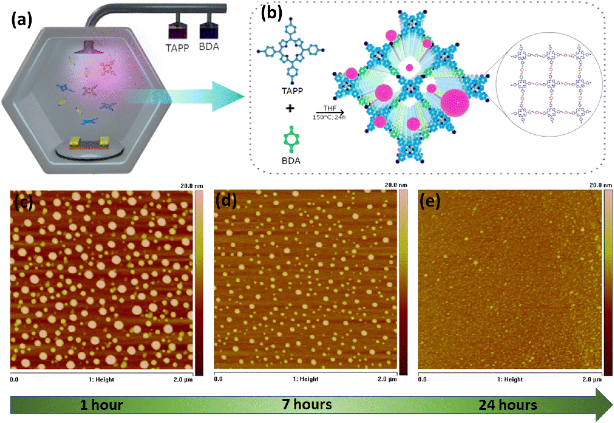 | ||
| Fig. 1 Schematic diagram of the (a) CVD setup, (b) the growth process and the structure of COF366-QD thin-film (c–e) Atomic Force Microscopy images of COF-QD thin-films deposited at different growth times (c) 1 h, (d) 7 h and (e) 24 h. | ||
Device fabrication & characterization
The COF366-QD device was fabricated to test its viability for future applications. The device fabrication started on an RCA cleaned p-type Si wafer, deposited with 500 nm SiO2 acting as an insulator layer and nucleation center for the growth of COF-QD thin films. Then, metal Cr/Au (10/120 nm) was deposited and patterned as interdigitated electrodes with distance of 5 μm. The COF-366-QD thin-film was then deposited on this patterned device as explained in the above section by chemical vapor deposition (CVD) under controlled and optimized conditions using S3 (24 h) CVD conditions. The CVD-grown thin film of the COF366-QD layer act as a photoactive layer in the horizontal Au-COF366QD-Au device structure. The chemical structure of the COF366-QD thin films was evaluated using FTIR (Bruker Vortex 80), XRD (Rigaku Smartlab 9kW) and XPS (Kratos Analytical, AXIS Supra). The surface topology and thickness of the COF366-QD film were analyzed using AFM Atomic force microscopy (AFM) [Bruker Multimode Nanoscope IV system] while TEM & HRTEM imaging of the films was performed using JEOL 2100F system. The electrical measurements were done using Keithley 2410 source meter using the SUSS MicroTec probe station with 145 Keysight B1500A Semiconductor Device Analyzer. Meanwhile, the optoelectrical measurements of the fabricated COF366-QDs based device were done using an in-house experimental set-up utilized with a 514 nm wavelength visible light source.Results and discussion
Structure and morphology characterization
Fig. 2a shows the experimental PXRD pattern of the CVD fabricated COF366 film compared with simulated COF-366 thin-film which are in good agreement with each other. The PXRD shows three distinct reflection peaks at 2θ = 3.7°, 6.7° and 16.7° which can be attributed to (100), (200) and (001) facets respectively, and matches well with previous reports.54,59,60 These well-defined diffraction peaks clearly indicate that COF thin film has an ordered and crystalline framework. Fig. 2b shows the comparative FTIR spectra of the BDA coated, TAPP coated and COF366-QD thin film deposited on silicon substrate respectively. As shown, the typical peaks at 1258 cm−1 and 1590 cm−1 have been observed can be ascribed to the characteristic C![[double bond, length as m-dash]](https://www.rsc.org/images/entities/char_e001.gif) N stretching, while it was also noted that the presence of the amino group of TAPP (3200–3500 cm−1) was significantly reduced in the COF366-QD film, indicating the development of the imine group and the creation of monomer linkages into the COF layer.55,61 The slight shift of CN (1590 cm−1) stretching frequency can be ascribed to strong covalent interactions between the COF and the QDs and thus indicate that QDs are effectually attached to the COF surface.62 Fig. 2c shows the UV-vis diffuse reflectance spectra of COF-366-QDs thin-film. As seen in the figure, the thin-film shows the characteristic absorbance peaks are observed at 470 nm [Soret (S) band] and 575 nm [Q band].58 The slight redshift of the absorption edges observed may be due to the presence of QD's in the COF thinfilm. To further understand the structural information of the COF366-QDs film, it was examined by high-resolution X-ray photoelectron spectra (XPS). Interestingly, we observed an emergent peak at 398.6 eV (N 1s) which can be assigned to CN strongly suggesting the formation of imine bonding in the COF layer (Fig. 3a). Another peak with higher binding energy and a minor peak at around 397.7 eV and 400.3 eV was observed representing non-protonated nitrogen structure and Ph-NH2 of porphyrin in the deposited COF thin film while the peak observed at 284.7 eV and 285.8 eV indicates the CC and C–N bond in C 1s spectrum of COF-QDs film respectively (Fig. 3b).55,58
N stretching, while it was also noted that the presence of the amino group of TAPP (3200–3500 cm−1) was significantly reduced in the COF366-QD film, indicating the development of the imine group and the creation of monomer linkages into the COF layer.55,61 The slight shift of CN (1590 cm−1) stretching frequency can be ascribed to strong covalent interactions between the COF and the QDs and thus indicate that QDs are effectually attached to the COF surface.62 Fig. 2c shows the UV-vis diffuse reflectance spectra of COF-366-QDs thin-film. As seen in the figure, the thin-film shows the characteristic absorbance peaks are observed at 470 nm [Soret (S) band] and 575 nm [Q band].58 The slight redshift of the absorption edges observed may be due to the presence of QD's in the COF thinfilm. To further understand the structural information of the COF366-QDs film, it was examined by high-resolution X-ray photoelectron spectra (XPS). Interestingly, we observed an emergent peak at 398.6 eV (N 1s) which can be assigned to CN strongly suggesting the formation of imine bonding in the COF layer (Fig. 3a). Another peak with higher binding energy and a minor peak at around 397.7 eV and 400.3 eV was observed representing non-protonated nitrogen structure and Ph-NH2 of porphyrin in the deposited COF thin film while the peak observed at 284.7 eV and 285.8 eV indicates the CC and C–N bond in C 1s spectrum of COF-QDs film respectively (Fig. 3b).55,58
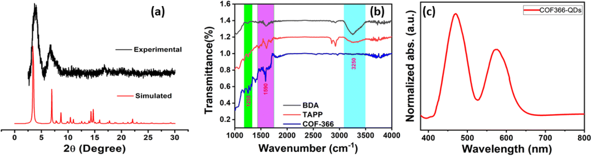 | ||
| Fig. 2 (a) The experimental PXRD pattern of chemical vapor deposited COF366 thin-film compared with simulated COF366 thin-film (b) FTIR spectra of the BDA (Black), TAPP (Red), and COF366 thin-film (Blue) (c) UV-vis diffuse reflectance spectra of COF-366-QDs thin-film. | ||
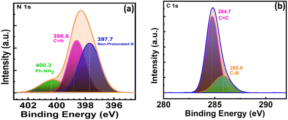 | ||
| Fig. 3 (a) Shows the XPS scan spectra of N 1s and (b) shows C 1s of COF366 thin-film. | ||
The surface topology analysis of the thin-film (S3) was studied by atomic force microscopy as shown in Fig. 4a–c and the average thickness of the COF366-QD thin film was found to be ∼112 nm (Fig. 4a). The thin film was observed to be homogeneously distributed on the Si surface and has uniform size distribution ranging from 0.5 nm to 2.2 nm (Fig. 4b) and the lateral size of the QDs is ∼2.5–3 nm (Fig. 4c). Next, the nanomorphology of the film was characterized by TEM and high-resolution transmission electron microscopy (HRTEM). The TEM images [Fig. 4c–f] clearly show the formation of the periodic, crystalline framework of the COF layer with monodispersed dark spots marked in white circles. The marked dark spots Fig. 4e display very good contrast change with the background COF layer, there can be seen spherical dark spots of several sizes, and the crystal structure of the dots exhibits sharp boundary with no aggregation, indicating the presence of quantum dots (QDs) embedded in the COF layer. The high-resolution TEM (HRTEM) (Fig. 4f) shows the porous framework of the COF layer while the entire surface of the layer is covered by uniformly distributed embedded QDs with good dispersity. The COF thin-film shows the self-organized distribution of QDs with the absence of agglomerates. In the same lines of AFM, the average size of QDs were evaluated from HRTEM to be about ∼2.5–3 nm in diameter with a distinct lattice structure of 0.23 nm (inset Fig. 4f) confirming COF366-QD film to be the highly crystalline with uniformly distributed QDs embedded within the COF film.63–65 Further, the COF366-QD thin-film was studied using energy dispersive spectroscopy (EDS) mapping images to explore the elemental distribution. Fig. 4e–g exhibits the existence of C, O, and N, elements consistently dispersed in the COF366-QD layer, verifying that the COF366-QD layer was successfully grown on the Si substrate by the CVD process.
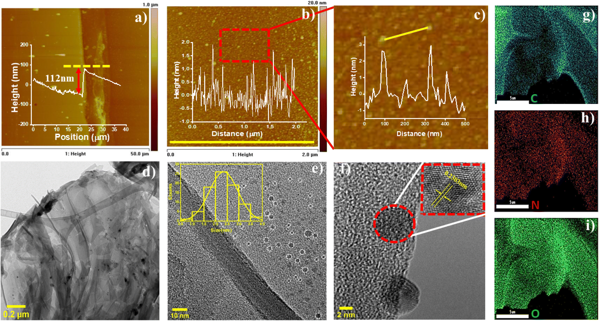 | ||
| Fig. 4 (a–c) AFM images and (d–f) Transmission electron micrograph of the in situ CVD deposited COF366-QDs thin-film; inset (e): the particle size distribution histograms with Gaussian fitting where the marked black dots indicate the Quantum dots embedded in the COF layer; inset (f) HRTEM image of the COFQDs and (g–i) EDS elemental mapping of the COFQD thin-film. | ||
The viability of the device as a photoactive device under visible light was tested for future applications (Fig. 5a). Here, Fig. 5b–d shows the typical current–voltage characteristics under dark and various illumination conditions of the fabricated device at room temperature. Fig. 5b inset shows the optical image of the fabricated device. A symmetric profile of current–voltage has been observed between forward and reverse bias conditions in the Au-COFQD-Au structure anticipated due to similar electrode work function. For zero bias condition, an incredibly low dark current of 4.36 × 10⁻¹¹ A was observed for the fabricated device. This considerable low dark current may be related to the Schottky barrier created by QDs at the interface due to which charge carriers are not able to overcome the barrier under dark and room temperature conditions. The photocurrent measurements of the device were obtained using a 514 nm laser with varying power levels. Under low illumination power (>0.48 μW), the open-circuit voltage (Voc) doesn't change much but as the illumination power increases to 0.56 μW, the Voc changes to +0.5 V indicating that the external applied voltage compensates for the built-in potential in the COF366-QD device. This observation is important since it shows that the embedded QDs in the COF layer play an effective role to harvest the visible-light energy and also act as an electron reservoir. Meanwhile, as the device was irradiated but no bias voltage applied, a small change in current is observed but as the illumination power increases to 0.56 μW, it is observed that the current increases to two orders of magnitude. However, as the bias voltage is applied in both forward and reverse bias, around 1.5 orders of magnitude of the current increase is observed for both bias regions, as the illumination power increases from 0.16 μW to 0.56 μW. Fig. 5d displays the enlarged section of the forward bias Region where the knee voltage in Region 1(0.5 to 1 V), Region 2 (1 V to 2 V), and Region 3 (2 V and above) condition was found to be 0.52 V, 1 V and 1.9 V respectively. Further, the double logarithmic I–V curve (forward bias) region (1,2 and 3) was fitted for 0.56 μW illumination as shown in the inset of Fig. 5d and the slopes were found to be ∼6.27, 3.30, and 1.55 respectively. This inferences that as the external voltage is applied and change in photon flux from Region 1 to Region 3, more photogenerated charge carriers are created, increasing the overall conductance which implies the onset of a new charge carrier mechanism and is apparently visible from the knee voltage change from one Region to another. For low voltage Regions (Region 1 and 2), slope ∼ 6.27 indicates that the current observes the trap-controlled space charge limited conduction (SCLC) with the formation of a conduction path between the electrodes through a network of embedded QDs in the COF layer.
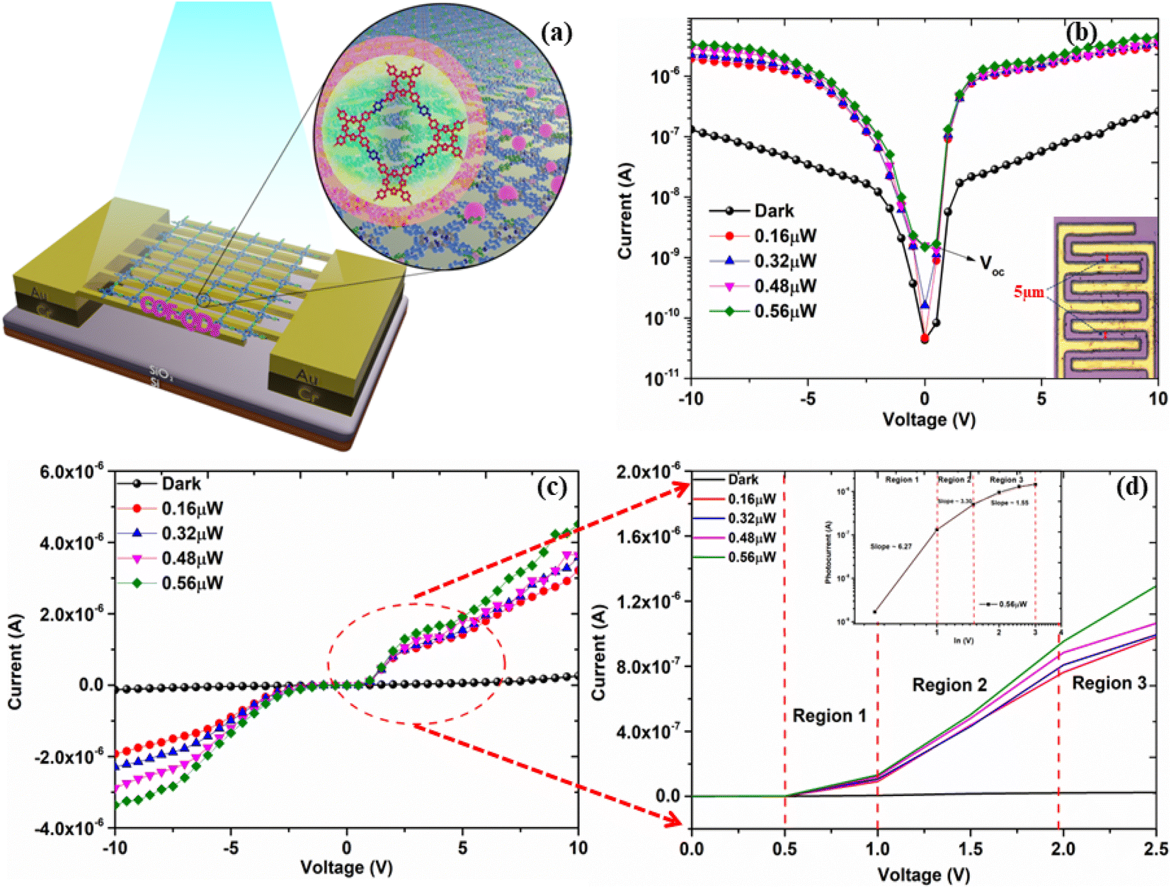 | ||
| Fig. 5 (a) Schematic representation of the fabricated device (b) semi-logarithmic current–voltage characteristics of COF366-QD device in the dark and upon irradiation with different power levels of 514 nm light; inset (b): shows the optical image of the fabricated device. (c and d) Linear current–voltage characteristics of the device where the forward bias Region is enlarged showing knee voltage in Region 1 to 3 and; inset (d): shows the double-logarithmic plot fitted for the forward bias current–voltage curve for Region 1 to 3 under 0.56 μW power. | ||
To attain further insight into the opto-electrical characteristics of the device, the power dependence of the photocurrent of the device with a 514 nm light source in reverse bias is shown in Fig. 6a. There is a steady increment in the photocurrent (Fig. 6a) while raising the incident light power up to 0.56 μW with no saturation. Meanwhile, it is also noteworthy that under −1 V and −3 V applied voltages, the current magnitude increase is much less compared to when higher voltages −7 V and −10 V are applied. It further confirms that when high voltages are applied, charge carriers from deep trap levels are pulled giving rise to higher magnitude of currents. As known, the photocurrent of the device is directly related to the photon flux on the device, providing critical information about the device performance such as responsivity. Here, Fig. 6b shows the power dependence of the photocurrent of the device at −10 V, and the value of responsivity is determined from the slope of Fig. 6b which is found to be 3.42 A W−1. To evaluate the responsive characteristics of the fabricated device, we further performed on-off switching experiments. The photocurrent response of the device was recorded under periodically chopped visible light at room temperature (Fig. 6c). The device showed a fast switch “ON” and “OFF” response to light irradiation with a significant increase in current as the biasing increased from 2 V (1.3 × 10⁻⁶A) to 5 V (2.9 × 10⁻⁶A) respectively. The switching response was very stable with very little variation as shown in Fig. 6c. The photogenerated charge carrier dynamics of the COF-366-QD device will be explored in the future scope of the paper. Thus, this device can be well utilized for high-incident power applications as a photonic sensor. Based on the above observations, the possible mechanisms in our COF366-QD thin-film based device can be illustrated by a simple schematic diagram Fig. 7a and b. The photocurrent generation mechanism of the COF366-QD photoactive layer can be expected as follows: (i) photocurrent generation at the COF/metal interface, (ii) light-induced charge carriers in the COF layer and QDs (iii) photocurrent generation due to traps in COF and trapped electrons in QDs. As the COF366-QD thin-film absorbs the incident visible photons, they create electron–hole pairs near the COF/Metal interface giving the instant photocurrent due to a smaller diffusion pathway between the adjacent metal electrodes. Further, the COF and QDs (away from the interface) also absorb incident photons and charge carriers of the highest occupied molecular orbital (HOMO) of COF were excited to the lowest unoccupied molecular orbital (LUMO) and similarly, photogenerated charge carriers are produced in the QDs also. Under the effect of the internal electric field, charge transfer between COF surface and QDs happens and the π–π stacking facilitates the charge transfer through a conduction path formation by a network of embedded QDs between the electrodes. These charge carriers drift towards the metal electrodes leading to the photocurrent as depicted by the observed photocurrent under various power levels at zero bias. However, there may be several defects present on the COF as well as QDs surface. The QDs are dispersed in the COF-366 layer in random order thus there is an energy barrier difference between COF LUMO and QD conduction band which assists the trapping of electrons in QDs. On absorption of visible photons, the electrons trapped in the COF, as well as QDs lower trap states, can be excited to higher trap states. These trapped electrons can move towards the metal electrode absorbing the visible photons under the built-in potential but the majority of them need externally applied bias voltage to move from the COFQD layer to the metal electrode. Previously, Yaghi and co-workers presented the linear I–V profile of a 2 μm width Au gap with a pure COF-366 layer.54 The pure COF-366 layer shows linear current–voltage behavior and doesn't show any knee voltage characteristics.
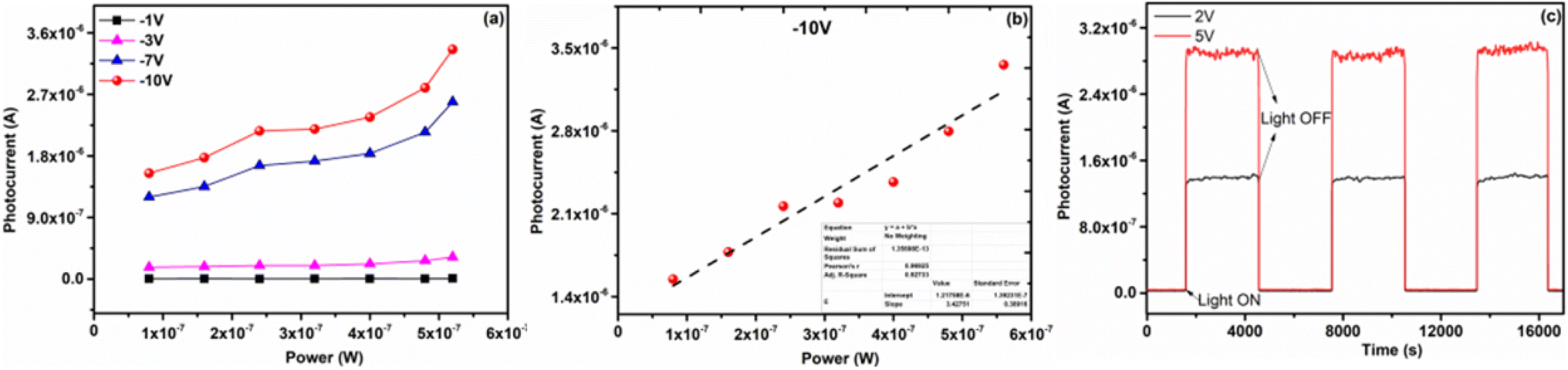 | ||
| Fig. 6 Photoresponse performance of the COF366-QD device (a) upon irradiation with different power of 514 nm visible light and bias voltages in reverse bias Region, (b) at −10 V (c) on/off switching of photocurrent at the bias voltage of 2 V and 5 V. | ||
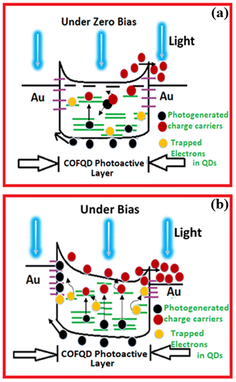 | ||
| Fig. 7 Schematic illustration of the proposed Au/COF366QD/Au device under (a) zero bias and (b) bias condition. | ||
Thus, it can be clearly inference that for our COF-366 with QDs based device, a clear rise in the current at the knee voltage observed in Regions 1, 2, and 3 proposes that as the bias voltage increases more and more trapped electrons from shallow and deep trap levels in the QDs are pulled by the bias voltage enhancing the overall current. However, as the applied voltage further increases (5 to 10 V), the trapped electrons are already being pulled from QDs and QDs trap states are probably empty, and thus saturation of the photocurrent is observed for higher voltages in forward as well as reverse bias Regions as seen in Fig. 5b. Thus, it can be understood that the QDs play a dominant role in the enhancement of the photocurrent of the COF366-QD layer in knee voltage regions due to the contribution of the added trapped electrons from QDs adding to the total current61,66,67
Conclusion
We have demonstrated a chemical vapor deposited COF366-QDs thin film device capable of responding to visible light illumination. FTIR and XPS studies show the formation of imine bonding in the thin-film. Our structural studies of the deposited film shows good crystalline porous framework of the COF layer along with mono-dispersed QDs with average size of about ∼2.5–3 nm in diameter. The photoactivity of this device was investigated under 514 nm visible light illumination and found to exhibit a good photocurrent 1.54 × 10⁻⁶ A with 0.08 μW minimum power. The device shows good on/off switching response stability. The proposed in situ CVD deposited COF366-QDs thin film provides an easy fabrication technique for large area growth of this photoactive material for various device applications. Our photoresponse studies suggest that the fabricated device can be effortlessly used as a photonic sensor, optoelectronic device and on-chip device applications.Conflicts of interest
There are no conflicts to declare.Acknowledgements
We acknowledge Govt. of India, Ministry of Science and technology, Department of Science and technology for Senior Research Fellowship grant DST/NM/NT/2018/150(G) for funding. We thank IITB Physics central facility for the use of AFM and XRD characterisation. We also thank CEN-IITB for technical support.Notes and references
- A. P. Cote, A. I. Benin, N. W. Ockwig, M. O'Keeffe, A. J. Matzger and O. M. Yaghi, Science, 2005, 310, 1166–1170 CrossRef CAS PubMed.
- H. Sahabudeen, H. Qi, B. A. Glatz, D. Tranca, R. Dong, Y. Hou, T. Zhang, C. Kuttner, T. Lehnert, G. Seifert, U. Kaiser, A. Fery, Z. Zheng and X. Feng, Nat. Commun., 2016, 7, 1–8 Search PubMed.
- Y. Yang, S. Mallick, F. Izquierdo-Ruiz, C. Schäfer, X. Xing, M. Rahm and K. Börjesson, Small, 2021, 17, 2103152 CrossRef CAS PubMed.
- K. Yang, W. Yuan, Z. Hua, Y. Tang, F. Yin and D. Xia, ACS Appl. Mater. Interfaces, 2019, 12, 3919–3927 CrossRef PubMed.
- Q. Gao, X. Li, G.-H. Ning, H.-S. Xu, C. Liu, B. Tian, W. Tang and K. P. Loh, Chem. Mater., 2018, 30, 1762–1768 CrossRef CAS.
- Y. Wu, D. Yan, Z. Zhang, M. M. Matsushita and K. Awaga, ACS Appl. Mater. Interfaces, 2019, 11, 7661–7665 CrossRef CAS PubMed.
- L. Sun, L. Li, J. Fan, Q. Xu and D. Ma, J. Mater. Sci. Technol., 2022, 123, 41–48 CrossRef.
- T. Li, H. Yu, Z. Xiong, Z. Gao, Y. Zhou and S.-T. Han, Mater. Horiz., 2021, 8, 2041–2049 RSC.
- C. Wang, Y. Wang, R. Ge, X. Song, X. Xing, Q. Jiang, H. Lu, C. Hao, X. Guo, Y. Gao and D. Jiang, Chem.–Eur. J., 2018, 24, 585–589 CrossRef CAS PubMed.
- Q. Hao, Z.-J. Li, C. Lu, B. Sun, Y.-W. Zhong, L.-J. Wan and D. Wang, J. Am. Chem. Soc., 2019, 141, 19831–19838 CrossRef CAS PubMed.
- S. Wan, J. Guo, J. Kim, H. Ihee and D. Jiang, Angew. Chem., Int. Ed., 2009, 48, 5439–5442 CrossRef CAS PubMed.
- R. Liu, K. T. Tan, Y. Gong, Y. Chen, Z. Li, S. Xie, T. He, Z. Lu, H. Yang and D. Jiang, Chem. Soc. Rev., 2021, 50, 120–242 RSC.
- L. Zhai, W. Wei, B. Ma, W. Ye, J. Wang, W. Chen, X. Yang, S. Cui, Z. Wu, C. Soutis, G. Zhu and L. Mi, ACS Mater. Lett., 2020, 2, 1691–1697 CrossRef CAS.
- J. Liu, F. Yang, L. Cao, B. Li, K. Yuan, S. Lei and W. Hu, Adv. Mater., 2019, 31, 1902264 CrossRef PubMed.
- H. Zhang, J. Zhou, G.-G. Shan, G.-F. Li, C.-Y. Sun, D.-X. Cui, X.-L. Wang and Z.-M. Su, Chem. Commun., 2019, 55, 12328–12331 RSC.
- H. Duan, P. Lyu, J. Liu, Y. Zhao and Y. Xu, ACS Nano, 2019, 13, 2473–2480 CAS.
- X. Xu, S. Wang, Y. Yue and N. Huang, ACS Appl. Mater. Interfaces, 2020, 12, 37427–37434 CrossRef CAS PubMed.
- L. Wang, B. Dong, R. Ge, F. Jiang and J. Xu, ACS Appl. Mater. Interfaces, 2017, 9, 7108–7114 CrossRef CAS PubMed.
- Y. Peng, Y. Huang, Y. Zhu, B. Chen, L. Wang, Z. Lai, Z. Zhang, M. Zhao, C. Tan, N. Yang, F. Shao, Y. Han and H. Zhang, J. Am. Chem. Soc., 2017, 139, 8698–8704 CrossRef CAS PubMed.
- J. Hynek, J. Zelenka, J. Rathouský, P. Kubàt, T. Ruml, J. Demel and K. Lang, ACS Appl. Mater. Interfaces, 2018, 10, 8527–8535 CrossRef CAS PubMed.
- S. Park, Z. Liao, B. Ibarlucea, H. Qi, H.-H. Lin, D. Becker, J. Melidonie, T. Zhang, H. Sahabudeen, L. Baraban, C.-K. Baek, Z. Zheng, E. Zschech, A. Fery, T. Heine, U. Kaiser, G. Cuniberti, R. Dong and X. Feng, Angew. Chem., 2020, 132, 8295–8301 CrossRef.
- D. Wang, Z. Zhang, L. Lin, F. Liu, Y. Wang, Z. Guo, Y. Li, H. Tian and X. Chen, Biomaterials, 2019, 223, 119459 CrossRef CAS PubMed.
- Y. Zhu, D. Zhu, Y. Chen, Q. Yan, C.-Y. Liu, K. Ling, Y. Liu, D. Lee, X. Wu, T. P. Senftle and R. Verduzco, Chem. Sci., 2021, 12, 16092–16099 RSC.
- P. Pachfule, A. Acharjya, J. Roeser, R. P. Sivasankaran, M.-Y. Ye, A. Brückner, J. Schmidt and A. Thomas, Chem. Sci., 2019, 10, 8316–8322 RSC.
- S. Ghosh, Y. Tsutsui, T. Kawaguchi, W. Matsuda, S. Nagano, K. Suzuki, H. Kaji and S. Seki, Chem. Mater., 2022, 34, 736–745 CrossRef CAS.
- X. Feng, L. Liu, Y. Honsho, A. Saeki, S. Seki, S. Irle, Y. Dong, A. Nagai and D. Jiang, Angew. Chem., 2012, 124, 2672–2676 CrossRef.
- H. Ding, J. Li, G. Xie, G. Lin, R. Chen, Z. Peng, C. Yang, B. Wang, J. Sun and C. Wang, Nat. Commun., 2018, 9, 1–7 CrossRef CAS PubMed.
- S. Haldar, D. Chakraborty, B. Roy, G. Banappanavar, K. Rinku, D. Mullangi, P. Hazra, D. Kabra and R. Vaidhyanathan, J. Am. Chem. Soc., 2018, 140, 13367–13374 CrossRef CAS PubMed.
- B. Sun, C.-H. Zhu, Y. Liu, C. Wang, L.-J. Wan and D. Wang, Chem. Mater., 2017, 29, 4367–4374 CrossRef CAS.
- S.-L. Cai, Y.-B. Zhang, A. B. Pun, B. He, J. Yang, F. M. Toma, I. D. Sharp, O. M. Yaghi, J. Fan, S.-R. Zheng, W.-G. Zhang and Y. Liu, Chem. Sci., 2014, 5, 4693–4700 RSC.
- L. K. Beagle, Q. Fang, L. D. Tran, L. A. Baldwin, C. Muratore, J. Lou and N. R. Glavin, Mater. Today, 2021, 51, 427–448 CrossRef CAS.
- S. Jhulki, J. Kim, I.-C. Hwang, G. Haider, J. Park, J. Y. Park, Y. Lee, W. Hwang, A. A. Dar, B. Dhara, S. H. Lee, J. Kim, J. Y. Koo, M. H. Jo, C.-C. Hwang, Y. H. Jung, Y. Park, M. Kataria, Y.-F. Chen, S.-H. Jhi, M.-H. Baik, K. Baek and K. Kim, Chem, 2020, 6, 2035–2045 CAS.
- J. Liu, W. Zan, K. Li, Y. Yang, F. Bu and Y. Xu, J. Am. Chem. Soc., 2017, 139, 11666–11669 CrossRef CAS PubMed.
- B. Nath, W.-H. Li, J.-H. Huang, G.-E. Wang, Z.-h. Fu, M.-S. Yao and G. Xu, CrystEngComm, 2016, 18, 4259–4263 RSC.
- J. W. Colson, A. R. Woll, A. Mukherjee, M. P. Levendorf, E. L. Spitler, V. B. Shields, M. G. Spencer, J. Park and W. R. Dichtel, Science, 2011, 332, 228–231 CrossRef CAS PubMed.
- M. Calik, F. Auras, L. M. Salonen, K. Bader, I. Grill, M. Handloser, D. D. Medina, M. Dogru, F. Löbermann, D. Trauner, A. Hartschuh and T. Bein, J. Am. Chem. Soc., 2014, 136, 17802–17807 CrossRef CAS PubMed.
- D. Bessinger, L. Ascherl, F. Auras and T. Bein, J. Am. Chem. Soc., 2017, 139, 12035–12042 CrossRef CAS PubMed.
- L. Cao, B. Guo, Y. Yu, X. Zhou, J. R. Gong and S. Lei, ACS Omega, 2019, 4, 18780–18786 CrossRef CAS PubMed.
- L. Yao, Y. Zhang, H.-X. Wang, Y. Guo, Z.-M. Zhuang, W. Wen, X. Zhang and S. Wang, J. Mater. Chem. A, 2020, 8, 8518–8526 RSC.
- H. Yu and D. Wang, J. Am. Chem. Soc., 2020, 142, 11013–11021 CrossRef CAS PubMed.
- Y. Xiong, Q. Liao, Z. Huang, X. Huang, C. Ke, H. Zhu, C. Dong, H. Wang, K. Xi, P. Zhan, F. Xu and Y. Lu, Adv. Mater., 2020, 32, 1907242 CrossRef CAS PubMed.
- C. S. Diercks, S. Lin, N. Kornienko, E. A. Kapustin, E. M. Nichols, C. Zhu, Y. Zhao, C. J. Chang and O. M. Yaghi, J. Am. Chem. Soc., 2018, 140, 1116–1122 CrossRef CAS PubMed.
- D. Burmeister, M. G. Trunk and M. J. Bojdys, Chem. Soc. Rev., 2021, 50, 11559–11576 RSC.
- J. W. Colson, J. A. Mann, C. R. DeBlase and W. R. Dichtel, J. Polym. Sci., Part A: Polym. Chem., 2015, 53, 378–384 CrossRef CAS.
- Y. Chen, H. Cui, J. Zhang, K. Zhao, D. Ding, J. Guo, L. Li, Z. Tian and Z. Tang, RSC Adv., 2015, 5, 92573–92576 RSC.
- C. Li, Y. Wang, Y. Zou, X. Zhang, H. Dong and W. Hu, Angew. Chem., 2020, 132, 9489–9493 CrossRef.
- Y. Zhang, W. Zhang, Q. Li, C. Chen and Z. Zhang, Sens. Actuators, B, 2020, 324, 128733 CrossRef CAS.
- Z. Meng, R. M. Stolz and K. A. Mirica, J. Am. Chem. Soc., 2019, 141, 11929–11937 CrossRef CAS PubMed.
- S. Spitzer, A. Rastgoo-Lahrood, K. Macknapp, V. Ritter, S. Sotier, W. M. Heckl and M. Lackinger, Chem. Commun., 2017, 53, 5147–5150 RSC.
- S. Hao, T. Zhang, S. Fan, Z. Jia and Y. Yang, Chem. Eng. J., 2021, 421, 129750 CrossRef CAS.
- R. P. Bisbey, C. R. DeBlase, B. J. Smith and W. R. Dichtel, J. Am. Chem. Soc., 2016, 138, 11433–11436 CrossRef CAS PubMed.
- D. D. Medina, J. M. Rotter, Y. Hu, M. Dogru, V. Werner, F. Auras, J. T. Markiewicz, P. Knochel and T. Bein, J. Am. Chem. Soc., 2015, 137, 1016–1019 CrossRef CAS PubMed.
- M. Liu, Y. Liu, J. Dong, Y. Bai, W. Gao, S. Shang, X. Wang, J. Kuang, C. Du, Y. Zou, J. Chen and Y. Liu, Nat. Commun., 2022, 13, 1–9 Search PubMed.
- S. Wan, F. Gandara, A. Asano, H. Furukawa, A. Saeki, S. K. Dey, L. Liao, M. W. Ambrogio, Y. Y. Botros, X. Duan, S. Seki, J. F. Stoddart and O. M. Yaghi, Chem. Mater., 2011, 23, 4094–4097 CrossRef CAS.
- B. Sun, J. Li, W.-L. Dong, M.-L. Wu and D. Wang, J. Phys. Chem. C, 2016, 120, 14706–14711 CrossRef CAS.
- S. Lin, C. S. Diercks, Y.-B. Zhang, N. Kornienko, E. M. Nichols, Y. Zhao, A. R. Paris, D. Kim, P. Yang, O. M. Yaghi and C. J. Chang, Science, 2015, 349, 1208–1213 CrossRef CAS PubMed.
- Y. Wang, X. Sun and Y. Wang, RSC Adv., 2022, 12, 16046–16050 RSC.
- Y. Li, Z. Ou, B. Liang, J. Yang, R. Chen, H. Qi, U. Kaiser, W. Hong, X. Chen, L. Du, W. Liu and Z. Zheng, Polymers, 2021, 13, 1561 CrossRef CAS PubMed.
- P. Zhu, S. Li, S. Zhou, N. Ren, S. Ge, Y. Zhang, Y. Wang and J. Yu, J. Chem. Eng., 2021, 420, 127559 CrossRef CAS.
- S. Kandambeth, D. B. Shinde, M. K. Panda, B. Lukose, T. Heine and R. Banerjee, Angew. Chem., Int. Ed., 2013, 52, 13052–13056 CrossRef CAS PubMed.
- C. Zhao, L. Zhang, Q. Wang, L. Zhang, P. Zhu, J. Yu and Y. Zhang, ACS Appl. Mater. Interfaces, 2021, 13, 20397–20404 CrossRef CAS PubMed.
- T. Ni, D. Zhang, J. Wang, S. Wang, H. Liu and B. Sun, Sens. Actuators, B, 2018, 269, 340–345 CrossRef CAS.
- M. Zhang, Y. Li, L. Ma, X. Guo, X. Li, K. Li, X. Wang, C. Xia and S. Li, Chem. Commun., 2020, 56, 880–883 RSC.
- G. Meng, L. Zhen, S. Sun, J. Hai, Z. Zhang, D. Sun, Q. Liu and B. Wang, J. Mater. Chem. A, 2021, 9, 24365–24373 RSC.
- Y. Zhang, D. Zhang and H. Liu, Polymers, 2019, 11, 708 CrossRef CAS PubMed.
- L. Sun, L. Li, J. Yang, J. Fan and Q. Xu, Chin. J. Catal., 2022, 43, 350–358 CrossRef CAS.
- L. Wang, G. Huang, L. Zhang, R. Lian, J. Huang, H. She, C. Liu and Q. Wang, J. Energy Chem., 2022, 64, 85–92 CrossRef CAS.
| This journal is © The Royal Society of Chemistry 2023 |