
High-performance perovskite light-emitting diodes based on grain boundary passivation: progress, challenges and perspectives
Yalian
Weng
,
Eng Liang
Lim
 ,
Yuanyuan
Meng
,
Junpeng
Lin
and
Zhanhua
Wei
*
,
Yuanyuan
Meng
,
Junpeng
Lin
and
Zhanhua
Wei
*
Xiamen Key Laboratory of Optoelectronic Materials and Advanced Manufacturing, Institute of Luminescent Materials and Information Displays, College of Materials Science and Engineering, Huaqiao University, Xiamen 361021, China. E-mail: weizhanhua@hqu.edu.cn
First published on 27th September 2023
Abstract
Metal halide perovskites are emerging as promising candidates for next-generation display and lighting technologies. In less than 10 years, the external quantum efficiency (EQE) of perovskite light-emitting diodes (PeLEDs) has skyrocketed from 0.1% to around 30%. Herein, we briefly introduce PeLEDs and summarise our group's progress in preparing PeLEDs using the strategy of grain boundary passivation. Then, we present the challenges and future outlooks toward the further development of PeLEDs. We hope that this perspective can bring informative guidance and innovative ideas to the PeLED community.
1. Introduction
Metal halide perovskites with the chemical structure of ABX3 have attracted attention owing to their excellent optoelectrical properties, such as tunable emission wavelength, narrow full width at half-maximum (FWHM), long carrier diffusion length, high color purity and wide color gamut.1–5 Generally, A is a monovalent organic or inorganic cation, B is a divalent metallic cation, and X is a halide anion (e.g., A: Cs+, CH3NH3+ (MA+), CH(NH2)2+ (FA+); B: Pb2+, Sn2+; X: Cl−, Br−, I−).2,6,7 Since the first report of solution-processed PeLEDs that operated at room temperature in 2014,8 various types of strategies, i.e., additive engineering, interface engineering, composition engineering and so on, have been carried out to improve the performance and stability of PeLEDs. In just a decade of development, the maximum EQEs of the green, red and near-infrared-based PeLEDs have exceeded 20%.9–13 In this perspective, we introduce the working principle of PeLEDs and summarize our recent efforts in developing highly efficient PeLEDs with the EQE >20% through perovskite grain boundary passivation. At the same time, a detailed discussion of the challenges and the future outlooks toward the development of PeLEDs is also presented.2. Basic working principle of PeLEDs
PeLEDs can be categorized into p-i-n and n-i-p structures depending on the deposition sequence of the carrier transport layer (CTL) (Fig. 1(a) and (b)). When a forward voltage is applied to the device, the holes from the anode and the electrons from the cathode are injected into a hole transport layer (HTL) and an electron transport layer (ETL), respectively. Under an applied electric field, these charge carriers are drifted to a perovskite emitter layer and recombine radiatively, producing electroluminescence (Fig. 1(c)). The emission color or wavelength produced by PeLEDs depends on the energy bandgap (Eg) of the perovskite materials. For example, perovskite materials with iodide-dominant and chloride-dominant compositions can produce infrared and blue light, respectively. To minimize the exciton quenching and non-radiative recombination of the PeLEDs, it is essential to optimize (i) the quality of the perovskite film, (ii) the charge injection into PeLEDs, (iii) the energy level alignment, (iv) the interface contact, and (v) the physical and chemical properties of each functional layer. Through electrical and optical characterization studies, the performance of PeLEDs, such as EQE, luminance and current efficiency, can be obtained.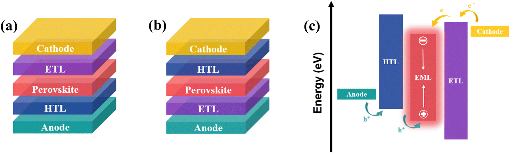 | ||
| Fig. 1 Typical structures of the PeLED device: (a) p-i-n structure and (b) n-i-p structure. (c) Schematic diagram of the electroluminescence mechanism of PeLEDs. | ||
3. Grain boundary passivation strategies
Nowadays, a spin-coating method has been widely used to prepare the perovskite films for optoelectronic applications. However, the perovskite films derived from the solution-processing methods usually exhibit poor surface coverage with a large number of bulk/surface defects attributed to the uncontrollable perovskite crystallization rate during the film formation process.14–17 To optimize the perovskite film quality with the enhanced electrical and chemical properties of PeLED applications, we have developed a series of grain boundary passivation strategies: halide passivation, non-halide passivation and their combination (Fig. 2). In the following subsections, we will introduce these strategies in detail for fabricating highly efficient and stable PeLEDs.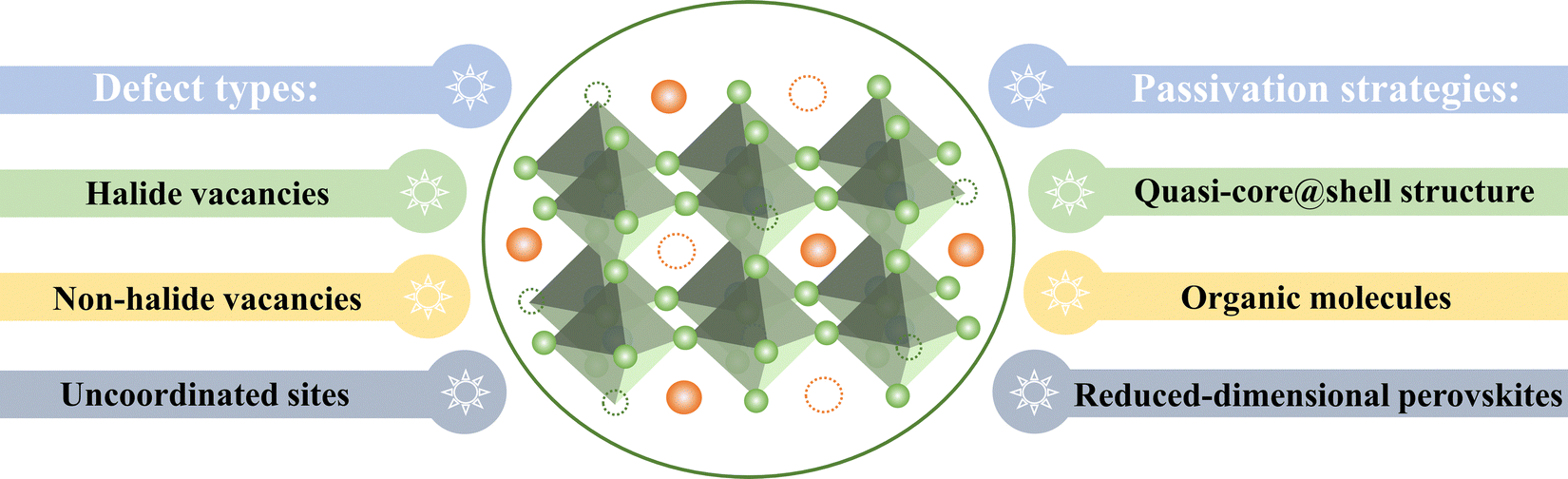 | ||
| Fig. 2 Defect classification of perovskite films and the corresponding grain boundary passivation strategies. | ||
3.1. Halide passivation
It is well-known that the number of defects/vacancies induced on the perovskite film surface/bulk film highly depends on the perovskite crystallization rate process. And it is hard to obtain a high-quality CsPbBr3 emitter layer due to its fast and uncontrollable crystallization.18–20 To overcome this problem, our group introduced the methylammonium bromide (MABr) additive to the CsPbBr3 perovskite precursor to modulate the corresponding crystallization process (Fig. 3(a)). Because of the very different solubility between CsPbBr3 and MABr in DMSO (CsPbBr3:∼0.56 M, MABr: >5 M), MABr could sequentially crystallize after the CsPbBr3 precursor was wholly consumed, yielding the CsPbBr3@MABr quasi-core@shell structure.9 In this study, we found that the addition of MABr not only passivated the perovskite surface and grain boundaries but also facilitated the balance charge injection into the PeLEDs. Benefitting from these, the non-radiative recombination of PeLEDs was suppressed, yielding higher photoluminescence efficiency with a longer device lifetime. To further improve the charge injection balance of PeLEDs, poly(methyl methacrylate) (PMMA) was spin-coated at the perovskite/B3PYMPM interface (Fig. 3(b)). A maximum EQE of 20.31% (Fig. 3(c)) with a T50 of more than 100 h (Fig. 3(d)) was achieved for the dual-modification device, which was the best-reported performing PeLED in 2018. | ||
| Fig. 3 (a) Formation process diagram of the CsPbBr3@MABr quasi-core@shell structure. (b) Structure of the PeLED device. (c) EQE–L characteristic and (d) lifetime measurement of the best-performing PeLEDs. Reproduced with permission from ref. 9. Copyright 2018, Springer Nature Limited. | ||
Encouraged by the performance enhancement from MABr, we concluded that halide salt could modulate the crystallization process and affect the as-formed film's morphology, composition and spatial distribution. However, MABr is an organic salt and may suffer from ion migration and decomposition issues when the PeLEDs are driven at a high voltage. Hence, we tried to use the more thermally stable formamidinium bromide (FABr). Interestingly, adding FABr to the perovskite precursor not only induced the quasi-core@shell structure formation but also initiated a chemical reaction and formed the Cs4PbBr6 interlayer. Benefited from the formation of CsPbBr3&Cs4PbBr6@MABr&FABr quasi-core@shell structure, the vacancy defects (i.e., Cs+ and Br−) and the non-radiative recombination center (i.e., uncoordinated Pb atom) of the CsPbBr3 perovskite were significantly suppressed.21 Additionally, Cs4PbBr6 with a suitable thickness can form a type-I heterojunction with CsPbBr3 to confine charge carriers in the CsPbBr3 crystals, increasing the radiative recombination efficiency (Fig. 4(a)). Therefore, the phase ratio of Cs4PbBr6 on CsPbBr3 was optimized to enhance the performance of perovskite films and devices (Fig. 4(b)). When the molar ratio of CsPbBr3:MABr:FABr was 1![[thin space (1/6-em)]](https://www.rsc.org/images/entities/char_2009.gif) :0.8:0.2, the PeLEDs (Fig. 4(d)) exhibited superior device performance (i.e., a maximum EQE of 22.3% and a higher luminance of 10050 cd m−2) with a longer device lifetime (i.e., T50 of 59 h at 130 cd m−2) (Fig. 4(c), (e), and (f)).
:0.8:0.2, the PeLEDs (Fig. 4(d)) exhibited superior device performance (i.e., a maximum EQE of 22.3% and a higher luminance of 10050 cd m−2) with a longer device lifetime (i.e., T50 of 59 h at 130 cd m−2) (Fig. 4(c), (e), and (f)).
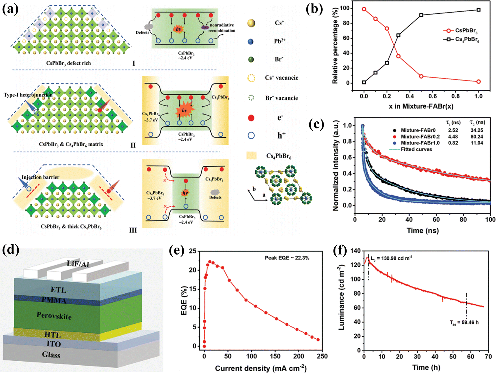 | ||
| Fig. 4 (a) Schematic illustration of the three typical phase compositions and their impact on defect passivation. (b) The relative percentages of CsPbBr3 and Cs4PbBr6 in various mixture perovskite films. (c) PL-decay curves of the three typical perovskite films. (d) Structure of the PeLED device. (e) EQE–J characteristics and (f) lifetime measurements of the best-performing PeLEDs. Reproduced with permission from ref. 21. Copyright 2022, Wiley-VCH GmbH. | ||
3.2 Non-halide passivation
In addition to halide-based materials, organic molecules, such as Lewis bases, Lewis acids, and alkylammonium salt, have also been widely used to passivate the ion defects and balance the charge injection of the perovskite emission layer.22–25 Currently, trioctylphosphine oxide (TOPO) and triphenylphosphine oxide (TPPO) are the commonly used non-halide passivator in PeLEDs. However, these organic molecules are insulators and not beneficial for the charge injection/charge transport in the devices.26,27 Aiming to solve this problem, our group proposed a bifunctional conductive molecule with two phosphine oxide functional groups, namely 2,7-bias (diphenylphosphoryl)-9,9′-spirobifluorene (SPPO13) as a passivation layer for CsPbBr3-based PeLED applications (Fig. 5(a)).28 With the addition of SPPO13, the P![[double bond, length as m-dash]](https://www.rsc.org/images/entities/char_e001.gif) O functional groups of SPPO13 could donate its lone electron pair on the oxygen atom to the empty 6p orbital of Pb2+ of the perovskite, thus, leading to the chemical changes of Pb2+ and Br− and the decrease of defect density. As a result, the surface defects of the perovskite were passivated, and the electron injection at the perovskite/ETL interface was promoted. Finally, the modified PeLEDs presented a maximum EQE of 22.3% with a maximum brightness of around 190000 cd m−2 (Fig. 5(b) and (c)).
O functional groups of SPPO13 could donate its lone electron pair on the oxygen atom to the empty 6p orbital of Pb2+ of the perovskite, thus, leading to the chemical changes of Pb2+ and Br− and the decrease of defect density. As a result, the surface defects of the perovskite were passivated, and the electron injection at the perovskite/ETL interface was promoted. Finally, the modified PeLEDs presented a maximum EQE of 22.3% with a maximum brightness of around 190000 cd m−2 (Fig. 5(b) and (c)).
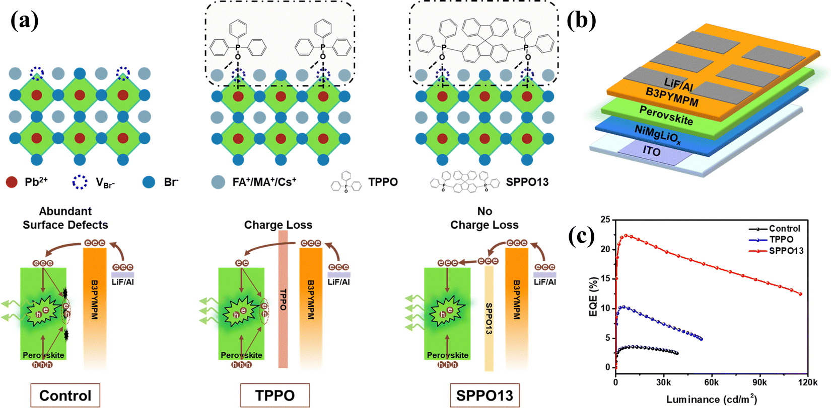 | ||
| Fig. 5 (a) Schematic illustration of the control, TPPO- and SPPO13-treated samples and the corresponding charge injection and recombination process. (b) Structure of the PeLED device. (c) EQE–L characteristics of the control, TPPO-treated and SPPO13-treated PeLEDs. Reprinted (adapted) with permission from ref. 28. Copyright 2022, American Chemical Society. | ||
Meanwhile, it has also been reported that polymers with different functional groups can interact with the perovskite grains to passivate the perovskite surface/bulk defects.29 For example, poly(vinylidene fluoride) (PVDF) with abundant F atoms was able to passivate both the organic cation and halide anion vacancies by forming hydrogen bonds (N–H⋯F) with organic cations (MA/FA) and ionic bonds with Pb2+ in the perovskite films, boosting the performance of PeLEDs.30 In contrast to the traditional surface treatment (Fig. 6(a)), our group recently showed that the infiltrative treatment method (Fig. 6(b)) enabled PVDF in the perovskite matrix to distribute on the perovskite grain boundary and the surface more evenly, increasing the PL intensity and lifetime of perovskite films (Fig. 6(c) and (d)). During the film formation process, the PVDF polymer could regulate the perovskite crystal growth and passivate the perovskite surface/bulk defects. Meanwhile, the film derived from the infiltrative treatment method exhibited a more compact film surface with tightly packed crystals. As a result, the non-radiative recombination and the energy loss were significantly suppressed. Finally, a maximum EQE of 22.29% with excellent reproducibility was achieved (Fig. 6(e), (f) and (g)).
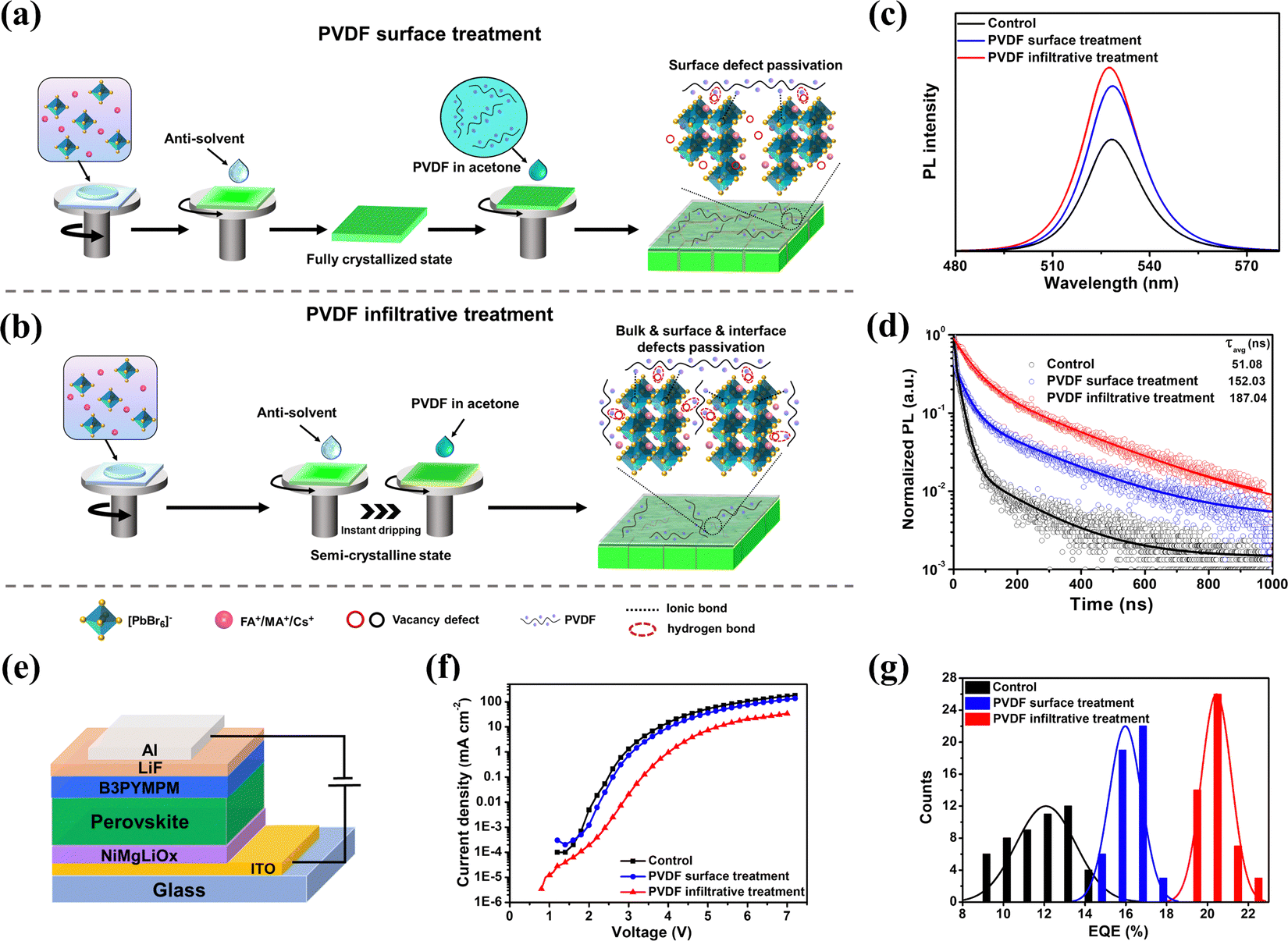 | ||
| Fig. 6 Schematic diagrams of treating perovskite films with PVDF via (a) surface treatment and (b) infiltrative treatment. The measurement of (c) steady PL spectra and (d) TRPL decay curves of the control, surface treatment, and infiltrative treatment films, respectively. (e) Structure of the PeLED device. (f) J–V characteristics and (g) EQE statistics histogram of the control, surface treatment, and infiltrative treatment PeLEDs. Reproduced with permission from ref. 30. Copyright 2022, Wiley-VCH GmbH. | ||
3.3 Combination of passivation strategies
3D perovskites can be transformed to quasi-2D perovskites (i.e., reduced dimensional perovskites (RDPs)) by adding large organic molecules into the A-site of 3D perovskites. Generally, RDPs consisting of quantum wells (QWs) separated by organic intercalating cations possess high exciton binding energies, which can increase the stability and the photoluminescence quantum yield (PLQY) of PeLEDs. However, the uneven QW thickness will induce energy disorders. Thus, RDP films show several problems of chaotic n value, different dimensions, non-radiative recombination defects and carrier transport difficulties, resulting in poor EQE with inferior color purity for RDP-based LEDs.To manipulate the crystallization rate of RDPs, we synthesized a bifunctional molecule containing fluorine atoms and a phosphine oxide (PO) functional group, namely tris (4-fluorophenyl) phosphine oxide (TFPPO). The TFPPO was dissolved in chloroform and then used as an antisolvent to modify the preparation of the PEA2Cs1.6MA0.4Pb3Br10 film.31 With TFPPO, the strong electronegativity of the F atom could form hydrogen bonds with the organic cations in the perovskite to serve as a diffusion controller during the RDP film formation process (Fig. 7(a)). On the other hand, phosphine oxide (PO) of TFPPO could bind to the unsaturated sites at the perovskite grain boundaries to reduce the defect density of the perovskite film. Benefitting from these, an enhanced PLQY with excellent device performance (i.e., a maximum EQE of 25.6%) was obtained for the modified PeLEDs (Fig. 7(b)), as well as a longer device lifetime (Fig. 7(c), (d) and (e)). This work highlights that the combination of macromolecular halogen ammonium salt (halide passivation) and organic passivation molecules (non-halide passivation) could provide a new pathway to improve the performance of PeLEDs.
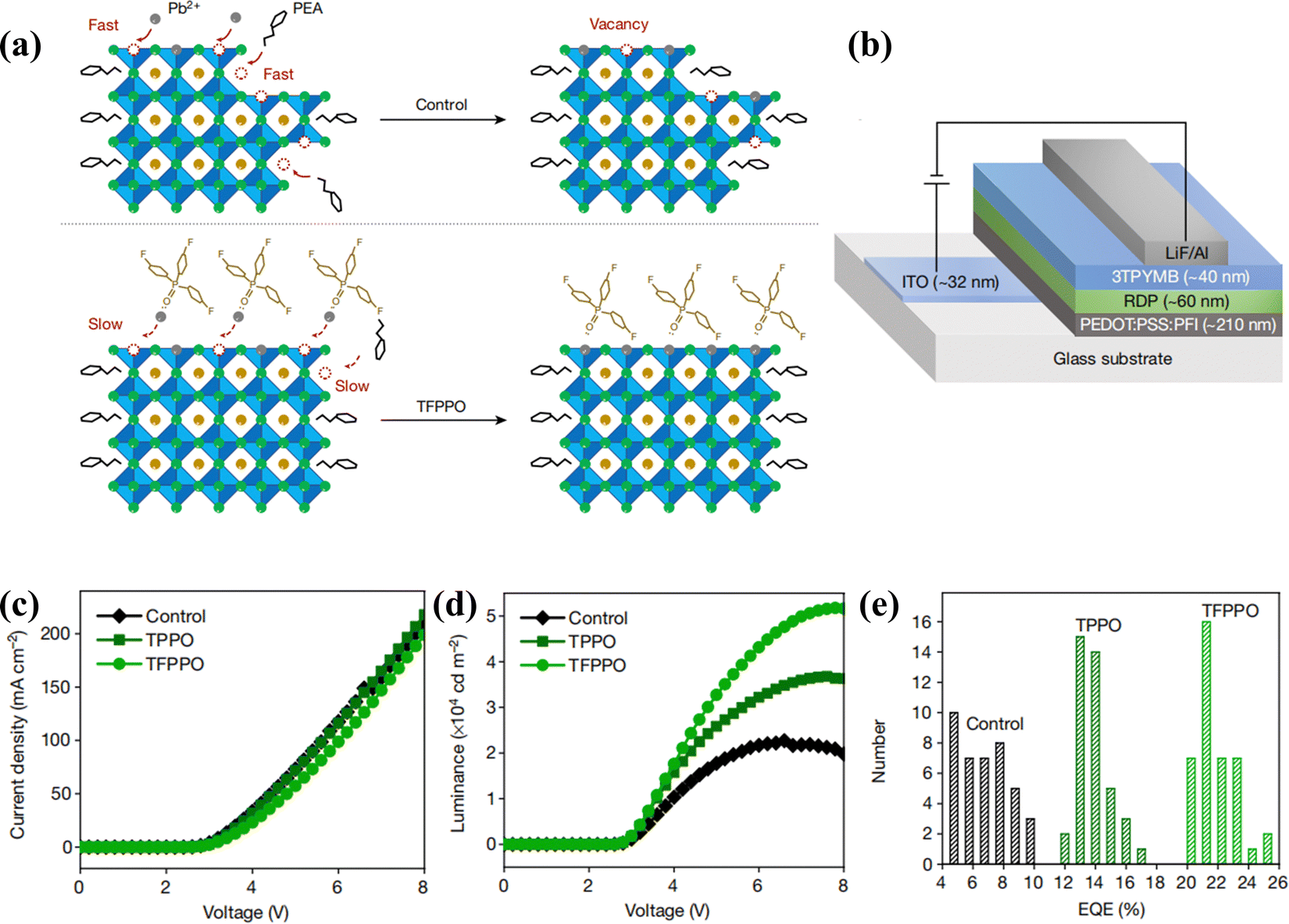 | ||
| Fig. 7 (a) Schematic illustration of the preparation of perovskite films with and without TFPPO. (b) Structure of the PeLED device. (c) J–V characteristics, (d) L–V characteristics and (e) EQE histogram of the control, TPPO-treated, and TFPPO-treated PeLEDs. Reproduced with permission from ref. 31. Copyright 2021, Springer Nature Limited. | ||
4. Challenges and perspectives of PeLEDs
Halide perovskites are excellent materials for research on perovskite solar cells (PSCs) and PeLEDs. Even though a high performance of 30.84% has been achieved for lead-based PeLEDs (Pb-PeLEDs),32 the toxicity of the lead (Pb) element in perovskites still remains a big challenge and can further hinder the development of PeLEDs. Meanwhile, the perovskite-based emission and functional layers also show poor ambient, thermal and light stability.33–38 To our knowledge, the operational stability of PeLEDs nowadays is excellently low compared to the inorganic LEDs, mostly due to the dissociation and ion migration of the perovskite material itself.33,39–41 To facilitate the commercialization of PeLEDs, the as-mentioned above issues need to be resolved.Because the Pb element in perovskites is harmful to humans and the environment, developing Pb-free PeLEDs is greatly important for PeLED applications. In general, Pb2+ can be replaced by Sn2+, Sb2+, Mn2+, Cu2+ and other elements.42 Among them, Sn2+ is considered as one of the potential candidates, which belongs to the same group element as Pb and has similar physical and chemical properties to those of Pb2+. Compared with Pb2+, Sn2+ possess a lower energy band gap and higher charge mobility. More importantly, SnO2, which degrades from Sn-based perovskites exposed to ambient air, is an environmentally friendly material that does not pollute the environment. Thus, we believe that the Sn-based perovskite emission layer will become a spot research material in PeLED applications. Recently, our group has achieved an impressive EQE of 5.4% based on the Sn-perovskite emitter (i.e., the highest recorded efficiency to date for CsSnI3 PeLEDs).43 However, the EQE of Sn-PeLEDs is much lower when compared with Pb-PeLEDs, attributed to the poor film morphology and the imbalance carrier transport of the Sn-based perovskite material, which needs to be further promoted. For the efficiency enhancement and stability improvement of PeLEDs, several promising strategies of device engineering (i.e., additive engineering, interface engineering, perovskite dimensionality manipulation and so on) are proposed as follows:
(I) Dimensionality manipulation: Typically, the non-radiative recombination rate is higher than the radiative recombination rate for three-dimensional (3D) perovskites, attributed to its lower exciton binding energy and longer carrier diffusion length. In contrast, the RDP exhibits excellent electrical properties, which is beneficial to facilitate the charge carrier injection into the perovskite emission layer.44,45 For example, it has been demonstrated that the natural quantum well 2D perovskite can limit the charge carrier within a specific region inside the emission layer. Due to the quantum restriction and dielectric confinement effect, the 2D perovskite exhibits higher exciton binding energy with excellent luminescence properties.44 Compared with 3D perovskites, 2D perovskites exhibit higher operational stability under light, thermal and ambient stress conditions. As such, it can be seen that manipulation of perovskite dimensionality is one of the effective methods to improve the performance and stability of PeLEDs.
(II) Additive engineering: It is generally accepted that slow nucleation and fast crystallization rates of the perovskite during the film formation process can induce a poor film morphology (i.e., many defective states) with lower fluorescence quantum efficiency. To regulate the crystallization rate and minimize the bulk/surface defect of perovskites, the addition of additives such as slow release agents and/or passivating agents (i.e., small organic molecules, polymers and metallic salts and so on) in the perovskite precursor solution and antisolvent solution during the film deposition process is proposed to control the precipitation of perovskite grains step by step or time by time (Fig. 8(a)), which is an effective way to boost the quality and photoelectric properties of perovskite films.
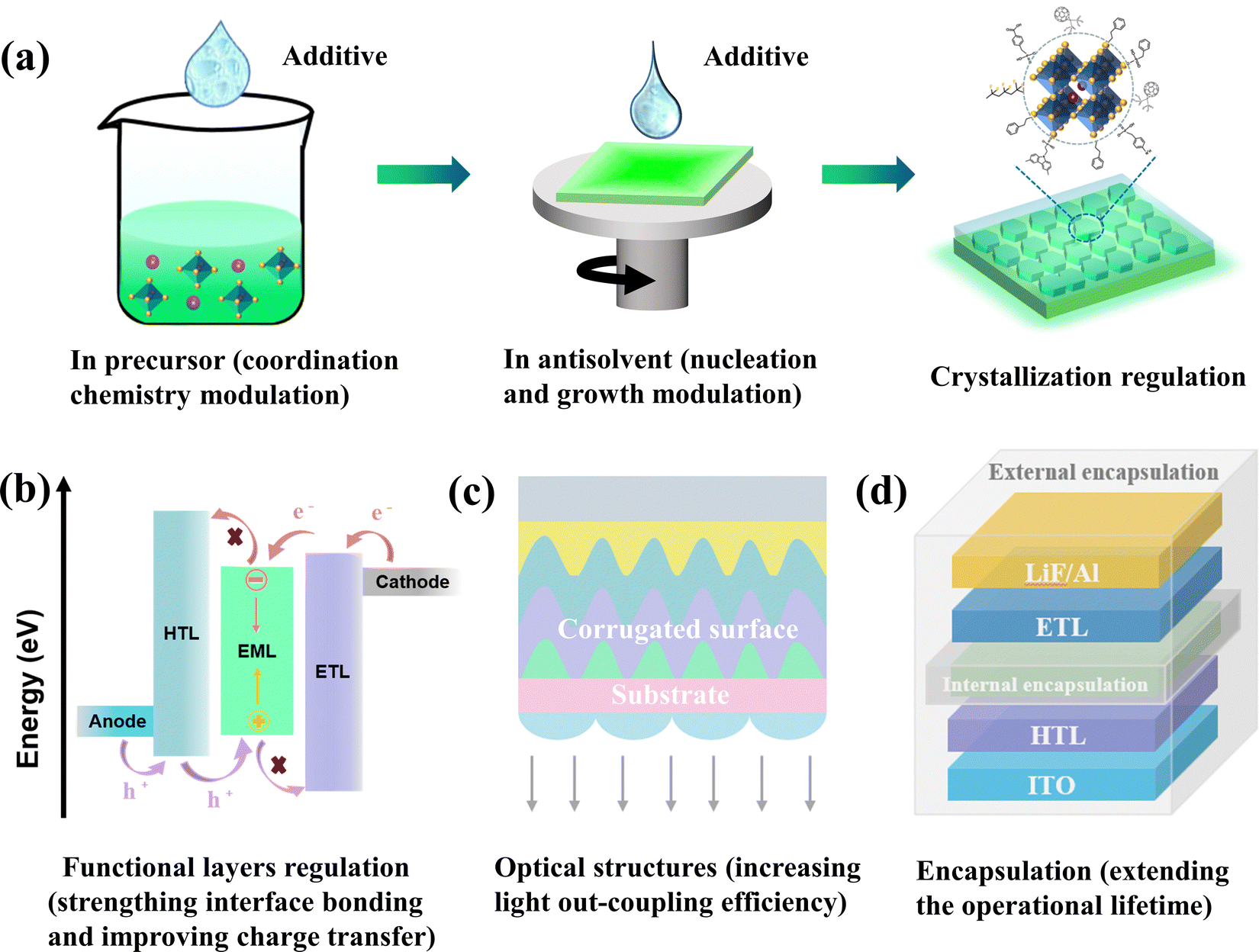 | ||
| Fig. 8 Strategy diagrams for improving the efficiency and stability of PeLEDs. (a) Additive engineering: introduce additives in the precursor or the antisolvent to regulate the crystallization process of perovskites. (b) Device structure: select suitable functional layers to improve radiative recombination. (c) Light extraction efficiency: adopt the corrugated surface or optical micro–nano structures to enhance the light out-coupling efficiency. (d) Internal and external encapsulations: encapsulate perovskite crystals or PeLED devices to increase the lifetime and stability. | ||
(III) Device structure modification: Each functional layer of PeLEDs has a crucial impact on the device performance and stability. Thus, it is important to carefully optimize the functional layer to optimize the charge carrier injection into the perovskite emission layer. For example, the conduction/valence band of ETL/HTL must well match with the lowest unoccupied molecular orbital (LUMO)/the highest occupied molecular orbital (HOMO) of perovskites so that the electrons/holes can be injected into the perovskite emitting layer effectively at a higher radiative recombination rate (Fig. 8(b)). In addition, modification at HTL/perovskite and perovskite/ETL interfaces can further reduce the trap states and the charge accumulation of PeLEDs. Taking advantages of these, lower non-radiative recombination loss with higher EQE of PeLEDs can be realized.
(IV) Light extraction efficiency optimization: It is well-known that the EQE of PeLEDs is determined by the internal quantum efficiency (IQE) and the light extraction efficiency (LEE), where the IQE can be increased to nearly 100% by optimizing the materials and device structures. However, the poor LEE of PeLEDs usually restricts the EQE of PeLEDs at <30%,13,46–48 attributed to the optical interaction between the various surfaces. A large number of photons are trapped or lost due to the total reflection and waveguide mode at the interface between air, functional layers and substrate, and the surface plasmon-polariton (SPP) mode at the metal cathode surface, unable to escape the device. Therefore, minimizing the total reflection, waveguide, and SPP modes of PeLEDs is important to increase the device's LEE performance. Various strategies are proposed to increase the light out-coupling efficiency, such as employing the wrinkle structure, nano-scattering layer, microlens arrays, optical structure and corrugated surface in PeLEDs (Fig. 8(c)). Improving the LEE will be the key to boosting EQE to over 30%.
(V) External and internal encapsulation: Perovskite materials are susceptible to water vapor and oxygen, leading to poor environmental stability. Therefore, it is crucial to encapsulate the PeLED device to protect them from external erosion. According to the location of the protective layer, encapsulation can be divided into internal encapsulation and external encapsulation, which are inside and outside the device, respectively (Fig. 8(d)). The internal encapsulation can be divided into upper and lower encapsulations according to its position relative to the perovskite material, which is essential for passivating surface defects, inhibiting ion migration, balancing charge injection and improving the stability of the perovskite emitting layer. By contrast, the external encapsulation can be divided into glass plate and thin film encapsulations, which are available for the flexible device. And the thin film encapsulation layer can be an inorganic layer, organic layer, or alternating inorganic–organic layer. Among them, the inorganic thin films (i.e., Al2O3, TiO2, ZrO2, Si3N4 and so on) serve as the main moisture/oxygen barrier, while the organic thin films (i.e., PMMA, PDMS, NOA and so on) are mainly responsible for filling the holes in the inorganic layer and prolonging the diffusion pathways for water vapor and oxygen. Generally, the inorganic layers can be obtained by atomic layer deposition (ALD), magnetron sputtering and thermal evaporation, while the organic layers can be prepared by spin coating, ink-jet printing, screen printing and other methods.
5. Conclusions
In conclusion, we have summarized our recent advances in high-performance PeLEDs using the grain boundary passivation strategy. Meanwhile, we also provide the challenges and future outlooks of PeLEDs. Even though highly efficient PeLEDs with an EQE of 30.84% have been realized, further efforts (i.e., perovskite dimension regulation, additive engineering, device structure design, encapsulation and light extraction efficiency improvement) are still required to further enhance the performance and stability of PeLEDs. Our group firmly believes that PeLEDs will serve as a promising technology for the next-generation displays and lighting in the future.Conflicts of interest
There are no conflicts to declare.Acknowledgements
This work was financially supported by the National Natural Science Foundation of China (62204089 and U21A2078), Natural Science Foundation of Fujian Province (2020J06021 and 2020J01064), the Promotion Program for Young and Middle-aged Teacher in Science and Technology Research of Huaqiao University (ZQN-1124) and the Scientific Research Funds of Huaqiao University (21BS132).References
- J. Zhang, P. P. Shum and L. Su, A review of geometry-confined perovskite morphologies: From synthesis to efficient optoelectronic applications, Nano Res., 2022, 15, 7402–7431 CrossRef CAS
.
- S. Z. Wang, J. T. Wang, Y. H. Lou, Y. H. Zhou and Z. K. Wang, Environment-Friendly Perovskite Light-Emitting Diodes: Progress and Perspective, Adv. Mater. Interfaces, 2022, 9, 2200772 CrossRef CAS
- S. Ju, Y. Zhu, H. Hu, Y. Liu, Z. Xu, J. Zheng, C. Mao, Y. Yu, K. Yang, L. Lin, T. Guo and F. Li, Dual-function perovskite light-emitting/sensing devices for optical interactive display, Light: Sci. Appl., 2022, 11, 331–339 CrossRef CAS PubMed
- A. Elattar, J. Kangsabanik, K. Nakao, K. Tsutsumi, H. Suzuki, T. Nishikawa, K. S. Thygesen and Y. Hayashia, Copper-incorporation for polytypism and bandgap engineering of MAPbBr3 perovskite thin films with enhanced near-Infrared photocurrent-response, Mater. Chem. Front., 2022, 6, 2690–2702 RSC
- Z. T. Li, H. W. Zhang, J. S. Li, K. Cao, Z. Chen, L. Xu, X. R. Ding, B. H. Yu, Y. Tang, J. Z. Ou, H. C. Kuo and H. L. Yip, Perovskite-Gallium Nitride Tandem Light-Emitting Diodes with Improved Luminance and Color Tunability, Adv. Sci., 2022, 9, 2201844 CrossRef CAS PubMed
- C. Otero-Martinez, J. Ye, J. Sung, I. Pastoriza-Santos, J. Perez-Juste, Z. Xia, A. Rao, R. L. Z. Hoye and L. Polavarapu, Colloidal Metal-Halide Perovskite Nanoplatelets: Thickness-Controlled Synthesis, Properties, and Application in Light-Emitting Diodes, Adv. Mater., 2022, 34, 2107105 CrossRef CAS PubMed
- Y. Xu, M. Cao and S. Huang, Recent advances and perspective on the synthesis and photocatalytic application of metal halide perovskite nanocrystals, Nano Res., 2021, 14, 3773–3794 CrossRef CAS
- Z. K. Tan, R. S. Moghaddam, M. L. Lai, P. Docampo, R. Higler, F. Deschler, M. Price, A. Sadhanala, L. M. Pazos, D. Credgington, F. Hanusch, H. J. Snaith and R. H. Friend, Bright lightemitting diodes based on organometal halide perovskite, Nat. Nanotechnol., 2014, 9, 687–692 CrossRef CAS PubMed
- K. Lin, J. Xing, L. N. Quan, F. P. G. de Arquer, X. Gong, J. Lu, L. Xie, W. Zhao, D. Zhang, C. Yan, W. Li, X. Liu, Y. Lu, J. Kirman, E. H. Sargent, Q. Xiong and Z. Wei, Perovskite light-emitting diodes with external quantum efficiency exceeding 20 percent, Nature, 2018, 562, 245–248 CrossRef CAS PubMed
- Y. Cao, N. Wang, H. Tian, J. Guo, Y. Wei, H. Chen, Y. Miao, W. Zou, K. Pan, Y. He, H. Cao, Y. Ke, M. Xu, Y. Wang, M. Yang, K. Du, Z. Fu, D. Kong, D. Dai, Y. Jin, G. Li, H. Li, Q. Peng, J. Wang and W. Huang, Perovskite light-emitting diodes based on spontaneously formed submicrometre-scale structures, Nature, 2018, 562, 249–253 CrossRef CAS PubMed
- T. Chiba, Y. Hayashi, H. Ebe, K. Hoshi, J. Sato, S. Sato, Y. J. Pu, S. Ohisa and J. Kido, Anion-exchange red perovskite
quantum dots with ammonium iodine salts for highly efficient light-emitting devices, Nat. Photon., 2018, 12, 681–687 CrossRef CAS
- Y. Dong, Y. K. Wang, F. Yuan, A. Johnston, Y. Liu, D. Ma, M. J. Choi, B. Chen, M. Chekini, S. W. Baek, L. K. Sagar, J. Fan, Y. Hou, M. Wu, S. Lee, B. Sun, S. Hoogland, R. Q. Bermudez, H. Ebe, P. Todorovic, F. Dinic, P. Li, H. T. Kung, M. I. Saidaminov, E. Kumacheva, E. Spiecker, L. S. Liao, O. Voznyy, Z. H. Lu and E. H. Sargent, Bipolar-shell resurfacing for blue LEDs based on strongly confined perovskite quantum dots, Nat. Nanotechnol., 2020, 15, 668–674 CrossRef CAS PubMed
- J. S. Kim, J. M. Heo, G. S. Park, S. J. Woo, C. Cho, H. J. Yun, D. H. Kim, J. Park, S. C. Lee, S. H. Park, E. Yoon, N. C. Greenham and T. W. Lee, Ultra-bright, efficient and stable perovskite light-emitting diodes, Nature, 2022, 611, 688–694 CrossRef CAS PubMed
- M. Qin, P. F. Chan and X. Lu, A Systematic Review of Metal Halide Perovskite Crystallization and Film Formation Mechanism Unveiled by In Situ GIWAXS, Adv. Mater., 2021, 33, 2105290 CrossRef CAS PubMed
- S. Tan, T. Huang and Y. Yang, Defect passivation of perovskites in high efficiency solar cells, J. Phys. Energy, 2021, 3, 042003 CrossRef CAS
- C. Yan, K. Lin, J. Lu and Z. Wei, Composition engineering to obtain efficient hybrid perovskite light-emitting diodes, Front. Optoelectron., 2020, 13, 282–290 CrossRef PubMed
- P. Barua and I. Hwang, Bulk Perovskite Crystal Properties Determined by Heterogeneous Nucleation and Growth, Materials, 2023, 16, 2110–2138 CrossRef CAS PubMed
- D. Zhang, Y. Fu, H. Zhan, C. Zhao, X. Gao, C. Qin and L. Wang, Suppressing thermal quenching via defect passivation for efficient quasi-2D perovskite light-emitting diodes, Light: Sci. Appl., 2022, 11, 69–78 CrossRef CAS PubMed
- J. K. Mishra, N. Yantara, A. Kanwat, T. Furuhashi, S. Ramesh, T. Salim, N. F. Jamaludin, B. Febriansyah, Z. E. Ooi, S. Mhaisalkar, T. C. Sum, K. Hippalgaonkar and N. Mathews, Defect Passivation Using a Phosphonic Acid Surface Modifier for Efficient RP Perovskite Blue-Light-Emitting Diodes, ACS Appl. Mater. Interfaces, 2022, 14, 34238–34246 CrossRef CAS PubMed
- M. Li, Y. Zhao, J. Guo, X. Qin, Q. Zhang, C. Tian, P. Xu, Y. Li, W. Tian, X. Zheng, G. Xing, W. H. Zhang and Z. Wei, Phase Regulation and Defect Passivation Enabled by Phosphoryl Chloride Molecules for Efficient Quasi-2D Perovskite Light-Emitting Diodes, Nano-Micro Lett., 2023, 15, 119–129 CrossRef CAS PubMed
- K. Lin, C. Yan, R. P. Sabatini, W. Feng, J. Lu, K. Liu, D. Ma, Y. Shen, Y. Zhao, M. Li, C. Tian, L. Xie, E. H. Sargent and Z. Wei, Dual-Phase Regulation for High-Efficiency Perovskite Light-Emitting Diodes, Adv. Funct. Mater., 2022, 32, 2200350 CrossRef CAS
- R. Yang, Y. Q. Li, M. L. Guo, X. Y. Cai and J. X. Tang, Efficient pure-red perovskite light-emitting diodes using dual-Lewis-base molecules for interfacial modification, J. Mater. Chem. C, 2021, 9, 9169–9177 RSC
- J. N. Yang, Y. Song, J. S. Yao, K. H. Wang, J. J. Wang, B. S. Zhu, M. M. Yao, S. U. Rahman, Y. F. Lan, F. J. Fan and H. B. Yao, Potassium Bromide Surface Passivation on CsPbI3-xBrx Nanocrystals for Efficient and Stable Pure Red Perovskite Light-Emitting Diodes, J. Am. Chem. Soc., 2020, 142, 2956–2967 CrossRef CAS PubMed
- S. Bonabi Naghadeh, B. Luo, G. Abdelmageed, Y. C. Pu, C. Zhang and J. Z. Zhang, Photophysical Properties and Improved Stability of Organic-Inorganic Perovskite by Surface Passivation, J. Phys. Chem. C, 2018, 122, 15799–15818 CrossRef CAS
- M. Lu, X. Zhang, X. Bai, H. Wu, X. Shen, Y. Zhang, W. Zhang, W. Zheng, H. Song and W. W. Yu, Spontaneous Silver Doping and Surface Passivation of CsPbI3 Perovskite Active Layer Enable Light-Emitting Devices with an External Quantum Efficiency of 11.2, ACS Energy Lett., 2018, 3, 1571–1577 CrossRef CAS PubMed
- X. Yang, X. Zhang, J. Deng, Z. Chu, Q. Jiang, J. Meng, P. Wang, L. Zhang, Z. Yin and J. You, Efficient green light-emitting diodes based on quasi-two-dimensional composition and phase engineered perovskite with surface passivation, Nat. Commun., 2018, 9, 570–577 CrossRef PubMed
- L. Na Quan, D. Ma, Y. Zhao, O. Voznyy, H. Yuan, E. Bladt, J. Pan, F. P. Garcia de Arquer, R. Sabatini, Z. Piontkowski, A. H. Emwas, P. Todorović1, R. Quintero-Bermudez, G. Walters, J. Z. Fan, M. Liu, H. Tan, M. I. Saidaminov, L. Gao, Y. Li, D. H. Anjum, N. Wei, J. Tang, D. W. McCamant, M. B. J. Roeffaers, S. Bals, J. Hofkens, O. M. Bakr, Z. H. Lu and E. H. Sargent, Edge stabilization in reduced-dimensional perovskites, Nat. Commun., 2020, 11, 170–178 CrossRef PubMed
- M. Li, Y. Zhao, X. Qin, Q. Ma, J. Lu, K. Lin, P. Xu, Y. Li, W. Feng, W. H. Zhang and Z. Wei, Conductive Phosphine Oxide Passivator Enables Efficient Perovskite Light-Emitting Diodes, Nano Lett., 2022, 22, 2490–2496 CrossRef CAS PubMed
- S. Wang, Z. Zhang, Z. Tang, C. Su, W. Huang, Y. Li and G. Xing, Polymer strategies for high-efficiency and stable perovskite solar cells, Nano Energy, 2021, 82, 105712 CrossRef CAS
- W. Feng, Y. Zhao, K. Lin, J. Lu, Y. Liang, K. Liu, L. Xie, C. Tian, T. Lyu and Z. Wei, Polymer-Assisted Crystal Growth Regulation and Defect Passivation for Efficient Perovskite Light-Emitting Diodes, Adv. Funct. Mater., 2022, 32, 2203371 CrossRef CAS
- D. Ma, K. Lin, Y. Dong, H. Choubisa, A. H. Proppe, D. Wu, Y. K. Wang, B. Chen, P. Li, J. Z. Fan, F. Yuan, A. Johnston, Y. Liu, Y. Kang, Z. H. Lu, Z. Wei and E. H. Sargent, Distribution control enables efficient reduced-dimensional perovskite LEDs, Nature, 2021, 599, 594–598 CrossRef CAS PubMed
- W. Bai, T. Xuan, H. Zhao, H. Dong, X. Cheng, L. Wang and R. J. Xie, Perovskite light-emitting diodes with an external quantum efficiency exceeding 30%, Adv. Mater., 2023 DOI:10.1002/adma.202302283
- L. Kong, X. Zhang, C. Zhang, L. Wang, S. Wang, F. Cao, D. Zhao, A. L. Rogach and X. Yang, Stability of Perovskite Light-Emitting Diodes: Existing Issues and Mitigation Strategies Related to Both Material and Device Aspects, Adv. Mater., 2022, 34, 2205217 CrossRef CAS PubMed
- V. J. Y. Lim, A. M. Ulatowski, C. Kamaraki, M. T. Klug, L. Miranda Perez, M. B. Johnston and L. M. Herz, Air-Degradation Mechanisms in Mixed Lead-Tin Halide Perovskites for Solar Cells, Adv. Energy Mater., 2022, 2200847 Search PubMed
- Y. Nakamura, N. Shibayama, K. Fujiwara, T. Koganezawa and T. Miyasaka, Degradation Mechanism of Halide Perovskite Crystals under Concurrent Light and Humidity Exposure, ACS Mater. Lett., 2022, 4, 2409–2414 CrossRef CAS
- P. Du, L. Gao and J. Tang, Focus on performance of perovskite light-emitting diodes, Front. Optoelectron., 2020, 13, 235–245 CrossRef PubMed
- J. T. Wang, S. Z. Wang, Y. H. Zhou, Y. H. Lou and Z. K. Wang, Flexible perovskite light-emitting diodes: Progress, challenges and perspective, Sci. China Mater., 2022, 66, 1–21 Search PubMed
- G. Li, K. Chen, Y. Cui, Y. Zhang, Y. Tian, B. Tian, Y. Hao, Y. Wu and H. Zhang, Stability of Perovskite Light Sources: Status and Challenges, Adv. Opt. Mater., 2020, 8, 1902012 CrossRef CAS
- N. Li, Y. Jia, Y. Guo and N. Zhao, Ion Migration in Perovskite Light-Emitting Diodes: Mechanism, Characterizations, and Material and Device Engineering, Adv. Mater., 2022, 34, 2108102 CrossRef CAS PubMed
- C. J. Tong, X. Cai, A. Y. Zhu, L. M. Liu and O. V. Prezhdo, How Hole Injection Accelerates Both Ion Migration and Non-radiative Recombination in Metal Halide Perovskites, J. Am. Chem. Soc., 2022, 144, 6604–6612 CrossRef CAS PubMed
- Q. Dong, L. Lei, J. Mendes and F. So, Operational stability of perovskite light emitting diodes, J. Phys.: Mater., 2020, 3, 012002 CAS
- S. Z. Wang, J. T. Wang, Y. H. Lou, Y. H. Zhou and Z. K. Wang, Environment-Friendly Perovskite Light-Emitting Diodes: Progress and Perspective, Adv. Mater. Interfaces, 2022, 9, 2200772 CrossRef CAS
- J. Lu, X. Guan, Y. Li, K. Lin, W. Feng, Y. Zhao, C. Yan, M. Li, Y. Shen, X. Qin and Z. Wei, Dendritic CsSnI3 for Efficient and Flexible Near-Infrared Perovskite Light-Emitting Diodes, Adv. Mater., 2021, 33, 2104414 CrossRef CAS PubMed
- L. Kong, X. Zhang, Y. Li, H. Wang, Y. Jiang, S. Wang, M. You, C. Zhang, T. Zhang, S. V. Kershaw, W. Zheng, Y. Yang, Q. Lin, M. Yuan, A. L. Rogach and X. Yang, Smoothing the energy transfer pathway in quasi2D perovskite films using methanesulfonate leads to highly efficient light-emitting devices, Nat. Commun., 2021, 12, 1246–1253 CrossRef CAS PubMed
- C. Sun, Y. Jiang, M. Cui, L. Qiao, J. Wei, Y. Huang, L. Zhang, T. He, S. Li, H. Y. Hsu, C. Qin, R. Long and M. Yuan, High-performance large-area quasi-2D perovskite light-emitting diodes, Nat. Commun., 2021, 12, 2207–2217 CrossRef CAS PubMed
- L. Gu, K. Wen, Q. Peng, W. Huang and J. Wang, Surface-Plasmon-Enhanced Perovskite Light-Emitting Diodes, Small, 2020, 16, 2001861 CrossRef CAS PubMed
- Q. Zhang, M. M. Tavakoli, L. Gu, D. Zhang, L. Tang, Y. Gao, J. Guo, Y. Lin, S. F. Leung, S. Poddar, Y. Fu and Z. Fan, Efficient metal halide perovskite light-emitting diodes with significantly improved light extraction on nanophotonic substrates, Nat. Commun., 2019, 10, 727–735 CrossRef PubMed
- Y. Miao, L. Cheng, W. Zou, L. Gu, J. Zhang, Q. Guo, Q. Peng, M. Xu, Y. He, S. Zhang, Y. Cao, R. Li, N. Wang, W. Huang and J. Wang, Microcavity top-emission perovskite light-emitting diodes, Light: Sci. Appl., 2020, 9, 89–94 CrossRef CAS PubMed
| This journal is © the Partner Organisations 2023 |