
 Open Access Article
 This Open Access Article is licensed under a Creative Commons Attribution-Non Commercial 3.0 Unported Licence
Small molecule dopant-free dual hole transporting material for conventional and inverted perovskite solar cells†‡
Miriam
Más-Montoya
 a,
Paula
Gómez
a,
Junke
Wang
b,
René A. J.
Janssen
*b and
David
Curiel
*a
a,
Paula
Gómez
a,
Junke
Wang
b,
René A. J.
Janssen
*b and
David
Curiel
*a
aMultifunctional Molecular Materials, Department of Organic Chemistry, Faculty of Chemistry, University of Murcia, Campus of Espinardo, 30100-Murcia, Spain. E-mail: davidcc@um.es
bMolecular Materials and Nanosystems, Institute for Complex Molecular Systems, Eindhoven University of Technology, P.O. Box 513, 5600 MB Eindhoven, The Netherlands. E-mail: r.a.j.janssen@tue.nl
First published on 27th June 2023
Abstract
Interfacial layers play very important roles in perovskite solar cells and the enormous diversity of reported materials has contributed to the outstanding progress of these photovoltaic devices. Nevertheless, the interfacial materials are commonly developed to be used in solar cells with a specific architecture, either conventional (n–i–p) or inverted (p–i–n). We report the exceptional performance of a small molecule, whose structural features, based on hydrogen bond-directed self-assembly, allow its application as hole transporting layer (HTL) in n–i–p and p–i–n perovskite solar cells with the same efficiency. This particularity has been investigated through a comparative study with a very similar molecule that cannot self-assemble, evidencing the benefits of the structural integrity of hydrogen bonded HTLs in terms of charge extraction and recombination, independently on the device architecture.
Introduction
Perovskite solar cells have become an emerging photovoltaic technology with promising prospects.1 The impressive improvement in the power conversion efficiency (PCE) along the last decade has reached a maximum value higher than 25%,2,3 which makes these devices an inspiring alternative for the development of future generation solar cells. The continuous progress in the performance of perovskite solar cells involves a multidisciplinary research effort seeking for the optimization of many different features such as perovskite composition, fabrication methods, and development of innovative materials (additives, passivating agents, dopants, hole transport layers, HTLs, and electron transport layers, ETLs).4 Moreover, this motivating evolution has been simultaneously achieved for the different architectures of perovskite solar cells, namely the conventional, n–i–p (mesoporous and planar),5,6 and the inverted, p–i–n (planar).7,8 In this regard, the stratified architecture of perovskite solar cells, essentially consisting of the external electrodes, the interfacial layers, and the active layer, has been a common design for the fabrication of these devices.9 To a great extent, the optimization of the efficiency has been achieved by exploring a plethora of interfacial layers, including both HTLs and ETLs.9 The critical importance of these layers is necessarily linked to the roles they play: (i) selective charge carrier extraction from the active layer; (ii) charge carrier transport to the electrodes; (iii) protection and stabilization of the perovskite active layer. To fulfil these functions, the interfacial layers must ideally meet certain requirements: (i) transparency to the solar radiation not to interfere with the absorption, at the active layer, of the incident sunlight or the light reflected within the solar cell; (ii) energy level alignment between the highest occupied molecular orbital (HOMO) and the valence band edge of the perovskite, in the case of HTLs, or the lowest unoccupied molecular orbital (LUMO) and the conduction band edge of the perovskite in the case of the ETLs; (iii) energy level alignment between the HOMO (LUMO) of the HTL (ETL) and the work function of the corresponding electrode (transparent or metallic) depending on the architecture of the solar cell, i.e., n–i–p or p–i–n; (iv) high LUMO energies, in the case of HTLs, or low HOMO energies, in the case of ETLs, to block wrongly directed charge carries within the solar cell; (v) good charge mobility to get a balanced transport of both holes and electrons; (vi) adequate film forming ability to avoid rough interfaces; (vii) compatible functionalization to interact with the perovskite interface. Given the abovementioned roles of the interfacial layers, all these features aim at the main objective of reducing the charge accumulation and recombination in the solar cell to improve its performance.Concerning the research about HTLs an immense diversity of materials has been reported.10,11 Excellent results have been achieved for different approaches related to inorganic materials12,13 and organic materials, where, in turn, we could make a difference between polymers and small molecules.14–17 Typically, these materials have been processed as thin films, but small molecules have lately gained much attention because of their integration as self-assembled monolayers.18–20 Focusing on the organic HTLs, the devices that have reached record efficiencies correspond to doped hole transporting materials. Although, this is not an unfavorable aspect of the perovskite solar cells, because the reported efficiencies are a proof of the validity of doped interfacial layers, the necessity of optimizing the devices with dopant-free HTLs has been convincingly argued. The reasons for that are related to the detrimental effect that dopants have on the chemical degradation of the perovskite layers and to the simplification on the number of components employed in the fabrication of the solar cells, affecting the fabrication protocol itself and the manufacturing costs. Accordingly, the development of dopant-free HTLs has become a very active research topic that has contributed to the progress of this technology.21–24 At this point, it is important to highlight that despite the myriad HTLs reported in the literature, these have been normally developed for a specific solar cell architecture, either n–i–p or p–i–n. Moreover, it is commonly found that those materials performing well for a certain architecture, do not perform equally well for the opposite architecture, as it was pointed out by Grisorio et al. a few years ago.25 In fact, very few precedents have been reported for hole transporting materials that lead to similar efficiencies in perovskite solar cells with conventional and inverted architectures.26 Certainly, this could be a very interesting approach for generalizing the fabrication methodologies of perovskite solar cells. Nevertheless, there are so many different aspects that affect the performance of solar cells (fabrication method and fabrication conditions, thin film properties, material and/or mixed materials purity and composition, to mention a few), and in some cases are so difficult to control, that it makes very intricate to find materials with dual applicability. A possible rational approach to this objective would require the use of materials whose structure is not affected when its thin film is processed in combination with different adjacent layers. As we have recently reported, the robustness of organic semiconductors can be enhanced by controlling their solid state structure through hydrogen-bond directed self-assembly.27–29 The strength of hydrogen bonding, within the context of non-covalent interactions, bestows the desired stability to the supramolecular self-organization of molecular materials. To further explore this hypothesis, we report herein a comparative study of two structurally related molecules, namely anthradi(7-azaindole), ADAI, and anthradiindole, ADI, (Fig. 1). Whereas ADAI presents a centrosymmetric structure with hydrogen bond donor and acceptor sites strategically located to set reciprocal hydrogen bonds, ADI, with a very similar centrosymmetric structure, lacks the hydrogen bond acceptor sites and cannot self-assemble through hydrogen bonding. Both molecules have been integrated as HTLs in perovskite solar cells with n–i–p and p–i–n architectures where we have observed an excellent consistency of the performance for the devices fabricated with the self-assembled material, ADAI, that has not been shown by the analogous ADI.
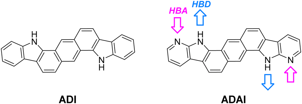 | ||
| Fig. 1 ADI and ADAI structures (HBA: hydrogen bond acceptor site; HBD: hydrogen bond donor site). | ||
Results and discussion
The synthesis of ADAI and ADI has been reported elsewhere.27 Their electronic structures have been determined through the combination of UV-vis spectroscopy and cyclic voltammetry. In this regard, the optical absorption bands are mainly located in the UV and extending towards the blue region of the visible spectrum (Fig. 2). Dissolved in dimethylformamide (DMF at 2.5 × 10⁻⁵ M), ADI and ADAI display two bands characteristic for fused polyaromatic systems: a strong band at about 335 nm and a less intense band at 420 nm, each with a superimposed fine structure resulting from coupling to the C![[double bond, length as m-dash]](https://www.rsc.org/images/entities/char_e001.gif) C stretch vibrations. In acenes these transitions are polarized along the long and short axes of the molecules, respectively.30 In thermally evaporated thin films, the spectra of ADI and ADAI are bathochromically shifted and more complex due to intermolecular interactions.31,32 For ADI, the first peak at 451 nm is relatively intense. This suggests J-type aggregation in which the short axes of adjacent chromophores are in a slipped co-facial orientation. This is in agreement with the 23–24° tilt angle of the connector between the centroids of the π–π stacked molecules and their short axes as inferred from the crystal structure (Fig. 4 and Fig. S1, ESI‡). For ADAI the long-wavelength absorption increases more slowly from its onset and reaches a first maximum at 427 nm. Such spectra are often indicative of H-type aggregation, in which chromophores are packed on top of each other, in agreement with a much larger tilt angle of 87–88° in the slipped-stack packing (Fig. 4 and Fig. S1, ESI‡). According to the onset of the lowest energy band, the thin films of both materials have a wide optical bandgap (ADAI: 2.68 eV; ADI: 2.63 eV), which makes these molecules virtually transparent to the visible and near-infrared radiation.
C stretch vibrations. In acenes these transitions are polarized along the long and short axes of the molecules, respectively.30 In thermally evaporated thin films, the spectra of ADI and ADAI are bathochromically shifted and more complex due to intermolecular interactions.31,32 For ADI, the first peak at 451 nm is relatively intense. This suggests J-type aggregation in which the short axes of adjacent chromophores are in a slipped co-facial orientation. This is in agreement with the 23–24° tilt angle of the connector between the centroids of the π–π stacked molecules and their short axes as inferred from the crystal structure (Fig. 4 and Fig. S1, ESI‡). For ADAI the long-wavelength absorption increases more slowly from its onset and reaches a first maximum at 427 nm. Such spectra are often indicative of H-type aggregation, in which chromophores are packed on top of each other, in agreement with a much larger tilt angle of 87–88° in the slipped-stack packing (Fig. 4 and Fig. S1, ESI‡). According to the onset of the lowest energy band, the thin films of both materials have a wide optical bandgap (ADAI: 2.68 eV; ADI: 2.63 eV), which makes these molecules virtually transparent to the visible and near-infrared radiation.
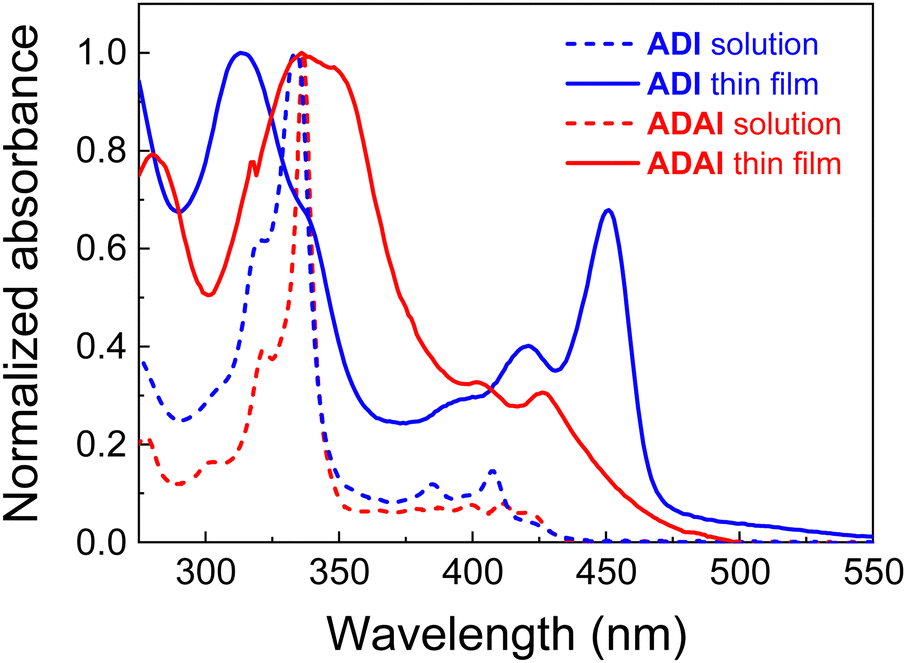 | ||
| Fig. 2 Normalized absorption spectra in DMF solution (2.5 × 10⁻⁵ M) and as thin films on quartz substrates, deposited by thermal evaporation in high vacuum (10−7–10−8 mbar). | ||
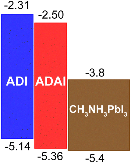
The cyclic voltammograms showed irreversible oxidation waves whose anodic onsets (ADAI: 1.00 V; ADI: 0.78 V) evidenced the electronic effect of the pyridine rings in the ADAI structure. In consequence, the HOMO energies estimated from the electrochemical data displayed a deeper value for ADAI (−5.36 eV) than ADI (−5.14 eV) (Table 1). By adding the energy of the optical bandgap to the HOMO energy, the LUMO energy was indirectly estimated (LUMOADAI: −2.50 eV; LUMOADI: −2.31 eV).
| λ onset (nm) | E opt. (eV) | E onset ox. (mV) | HOMOc (eV) | LUMOd (eV) | |
|---|---|---|---|---|---|
| a Thin film absorption spectrum. b E opt = 1240/λonset. c E HOMO = −e(Eonset ox. − Eonset ox. Fc/Fc+) + EHOMO Fc (Fc stands for ferrocene; Eonset ox. Fc/Fc+ = 0.44 V; EHOMO Fc = −4.8 eV). d E LUMO = EHOMO + Eopt. | |||||
| ADAI | 463 | 2.68 | 1000 | −5.36 | −2.50 |
| ADI | 471 | 2.63 | 776 | −5.14 | −2.31 |
Considering the architectures of the p–i–n and n–i–p solar cells where these molecules will be incorporated as HTLs, they both show suitable energy level alignment with the valence band of the CH3NH3PbI3 perovskite active layer that will be used in this case (Fig. 3), as well as with the work functions of the ITO (−4.7 eV) and gold (−5.1 eV) electrodes adjacent to the HTLs in the solar cells with inverted and conventional architectures respectively. Then, the interfacial energy gradient at both sides of the HTLs should favor hole extraction. Moreover, the depicted LUMO energies are high enough to block electrons generated in the active layer.
 | ||
| Fig. 3 Energy levels at the HTL/perovskite interface. | ||
The solid state structure of these molecules, determined by X-ray diffraction experiments, shows significant differences (Fig. 4). As intended, the 7-azaindole units integrated in the centrosymmetric ADAI structure promote the formation of reciprocal hydrogen bonds between the N–H in the pyrrole ring and the nitrogen in the pyridine ring. This results in a hydrogen-bonded ribbon-like structure that leads to a supramolecular organization of the conjugated molecules which are almost coplanar. Consequently, the π-stacking of adjacent ribbons produces a slipped-stack columnar arrangement where molecules are densely packed. When the crystal structure is expanded, neighbor ribbons define a highly ordered sequence of stacked molecules. Differently, ADI molecules pack following a herringbone pattern, mainly governed by edge-to-face (C–H⋯π and N–H⋯π) and face-to-face interactions. These differences in the crystal packing and the intermolecular contacts entail a higher density in the case of ADAI and should have an effect on the charge transport properties of these materials.
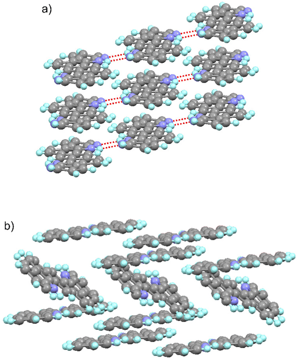 | ||
| Fig. 4 Crystal structures of (a) ADAI (dotted lines represent hydrogen bonds) and (b) ADI. | ||
The hole transporting ability of these materials was determined through the fabrication of single carrier devices with the architecture ITO/MoO3/HTM/MoO3/Ag. The current density vs. voltage (J–V) characteristics (Fig. S2, ESI‡) show the two transport regimes, namely ohmic (at lower applied voltages) and space charge-limited current (SCLC, at higher voltages). Hole mobilities are determined by fitting the SCLC range to the Murgatroyd equation.33 Interestingly, the mobility obtained for ADAI (μh = 1.1 × 10⁻⁴ cm2 V−1 s−1) is almost one order of magnitude higher than that determined for ADI (μh = 1.2 × 10⁻⁵ cm2 V−1 s−1), indicating that the molecular arrangement induced by hydrogen bond-directed self-assembly benefits the charge transport in ADAI. The higher mobility of this material can contribute to a better charge extraction when integrated into the solar cell architecture as it will be shown below.
To study the dual use of ADAI and ADI as HTLs and [6,6]-phenyl-C61-butyric acid methyl ester ([60]PCBM) as ETL in perovskite solar cells, devices with p–i–n architecture (ITO/HTL/CH3NH3PbI3/[60]PCBM/LiF/Al) and n–i–p architecture (ITO/SnO2/[60]PCBM/CH3NH3PbI3/HTL/MoO3/Au) were fabricated. The details for the fabrication of the solar cells are provided as ESI.‡ Additionally, we compared the performance of these dopant-free molecular materials to that of well-established HTLs in perovskite solar cells, such as poly(3,4-ethylenedioxythiophene) polystyrene sulfonate (PEDOT:PSS), for the inverted architecture, and 2,2′,7,7′-tetrakis[N,N-di(4-methoxyphenyl)amino]-9,9′-spirobifluorene (Spiro-MeOTAD), for the conventional one. It is worth mentioning that the formulation with polystyrenesulfonate makes that PEDOT:PSS can be considered as a self-doped polymer HTL. Similarly, the reference devices fabricated with Spiro-MeOTAD also included lithium bistrifluoromethanesulfonimidate (Li-TFSI), 4-tert-butylpyridine (TBP), and the cobalt complex FK209 as additives and dopants. The stabilized J–V characteristics for the best performing devices are represented in Fig. 5, (forward and reverse scans are displayed in Fig. S3, ESI‡) and the solar cell parameters are summarized in Table 2.
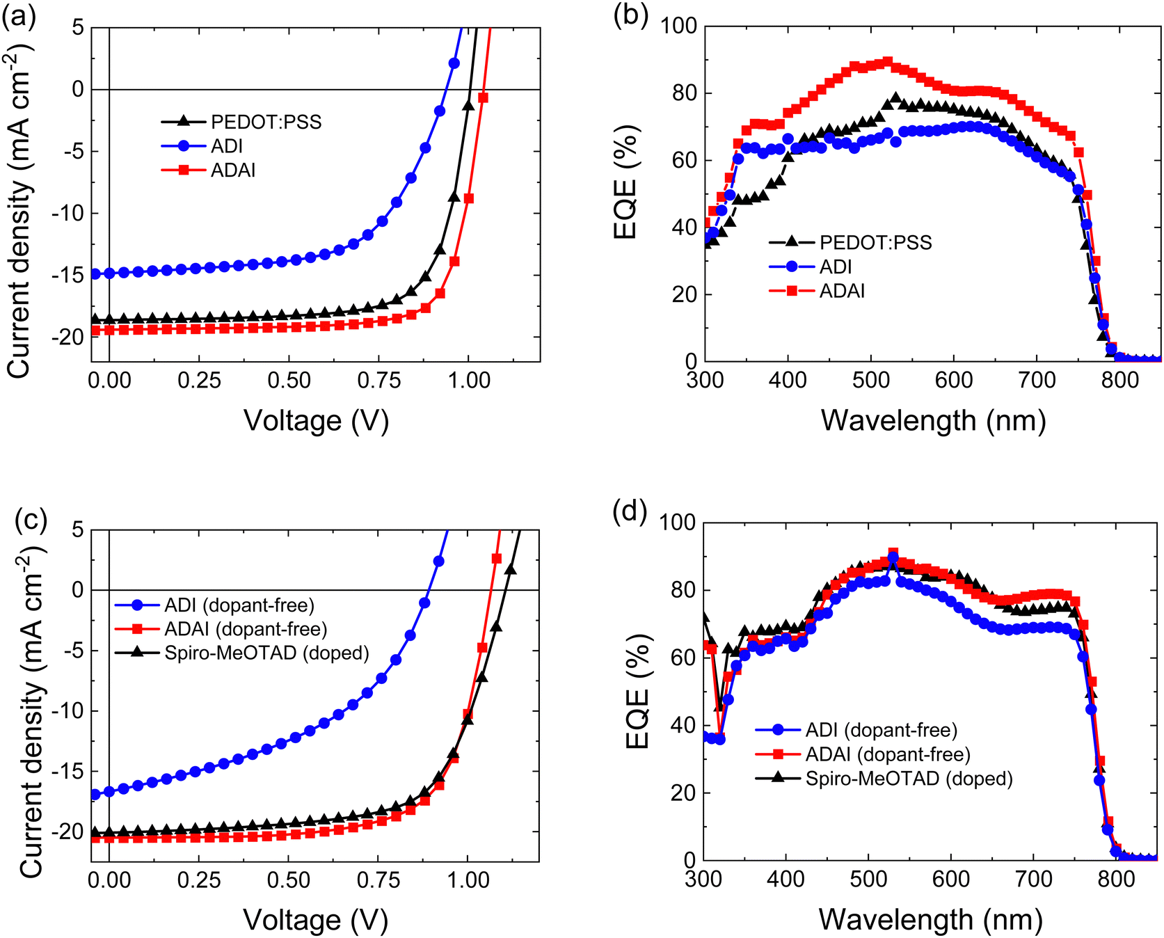 | ||
| Fig. 5 Stabilized J–V characteristics and external quantum efficiency (EQE) spectra for p–i–n (a and b) and n–i–p (c and d) architectures, respectively. | ||
| J SC (mA cm−2) | J SRSC (mA cm−2)a | V oc (V) | FF | PCE (%) | PCESR (%)b | HIc | |
|---|---|---|---|---|---|---|---|
| a J SRSC calculated by integration of the EQE spectrum with the AM1.5G spectrum. b PCESR calculated from JSRSC. Average parameters and standard deviation are given into brackets. c HI: hysteresis index. | |||||||
| p–i–n | |||||||
| PEDOT:PSS | 18.62 (18.48 ± 0.35) | 16.97 | 1.00 (0.96 ± 0.03) | 0.73 (0.76 ± 0.02) | 13.75 (13.51 ± 0.28) | 12.39 | 0.023 |
| ADI | 14.85 (15.52 ± 0.76) | 16.28 | 0.94 (0.90 ± 0.04) | 0.51 (0.57 ± 0.04) | 8.49 (7.64 ± 0.84) | 9.33 | 0.095 |
| ADAI | 19.40 (19.15 ± 0.19) | 19.88 | 1.04 (1.05 ± 0.01) | 0.77 (0.75 ± 0.02) | 15.50 (15.00 ± 0.48) | 15.92 | 0.027 |
| n–i–p | |||||||
| Spiro-MeOTAD (doped) | 20.09 (19.67 ± 0.59) | 20.24 | 1.11 (1.12 ± 0.01) | 0.66 (0.62 ± 0.06) | 14.76 (13.68 ± 1.53) | 14.83 | 0.007 |
| ADI | 16.68 (16.90 ± 0.44) | 18.77 | 0.89 (0.88 ± 0.02) | 0.44 (0.44 ± 0.02) | 6.61 (6.47 ± 0.50) | 7.35 | 0.147 |
| ADAI | 20.48 (20.33 ± 0.14) | 20.46 | 1.07 (1.08 ± 0.01) | 0.70 (0.66 ± 0.04) | 15.30 (14.73 ± 0.73) | 15.32 | 0.007 |
The results evidenced that the hydrogen-bonded material, ADAI, clearly outperformed its analog, ADI, in both architectures, showing higher open-circuit voltage (Voc), short-circuit current density (JSC), fill factor (FF), and power conversion efficiency (PCE), as well as much lower hysteresis index (HI).34 Besides, the most remarkable outcome of this investigation is the excellent uniformity of the solar cell performance incorporating ADAI as HTL, independently on the device architecture, as well as the better efficiencies reached in p–i–n and n–i–p devices, even when compared to the reference materials PEDOT:PSS and doped Spiro-MeOTAD. These features are ascribed to the particular structural and charge transporting properties that hydrogen bond-directed self-assembly bestows to the interfacial material. The similarity in the device performance between the p–i–n and n–i–p devices made using ADAI, suggests that there are no major differences in the ADAI layers deposited on ITO (in p–i–n) or on the perovskite (n–i–p). While the orientation of organic molecules in thin films may differ depending on the surface energy and roughness of the substrate,35,36 we previously found that this material does not alter its molecular organization when evaporated as thin film and hydrogen bonding is a useful driving force to obtain materials with consistent properties.27 The external quantum efficiency (EQE) spectra, acquired with bias illumination to simulate conditions corresponding to the standard solar spectrum (AM1.5G, 100 mW cm−2), showed a noticeably better photon-to-electron conversion in the p–i–n devices fabricated with ADAI when compared to ADI and PEDOT:PSS. These differences were still significant in the n–i–p devices when comparing ADAI to ADI, but only marginal when comparing ADAI and doped Spiro-MeOTAD, with the ADAI reaching a higher response for wavelengths above 650 nm. The integration of the EQE spectra led to JSRSC values that matched well those directly determined from the J–V curves.37 The higher quantum efficiencies are related to the larger JSC measured for ADAI.
The morphology of the HTLs and the perovskite layers was evaluated by atomic force microscopy (AFM) and scanning electron microscopy (SEM). The HTLs deposited onto ITO substrates exhibited similar morphological features with small round-shaped grains homogenously covering the entire substrate surface, which contrast to the featureless morphology of the PEDOT:PSS layer (Fig. 6a–c). A rougher surface was observed for the ADI films compared to both ADAI and PEDOT:PSS. As can be seen in the SEM images (Fig. 4d–f), these differences in the underlying HTL affect the morphology of the perovskite deposited atop. In this regard, the perovskite grown on PEDOT:PSS showed granular domains with different sizes that leave some voids at the grain boundaries (Fig. 4d).38 On the other hand, the perovskite layers deposited on the small molecular HTLs (Fig. 4e and f) exhibited a more compact surface morphology.
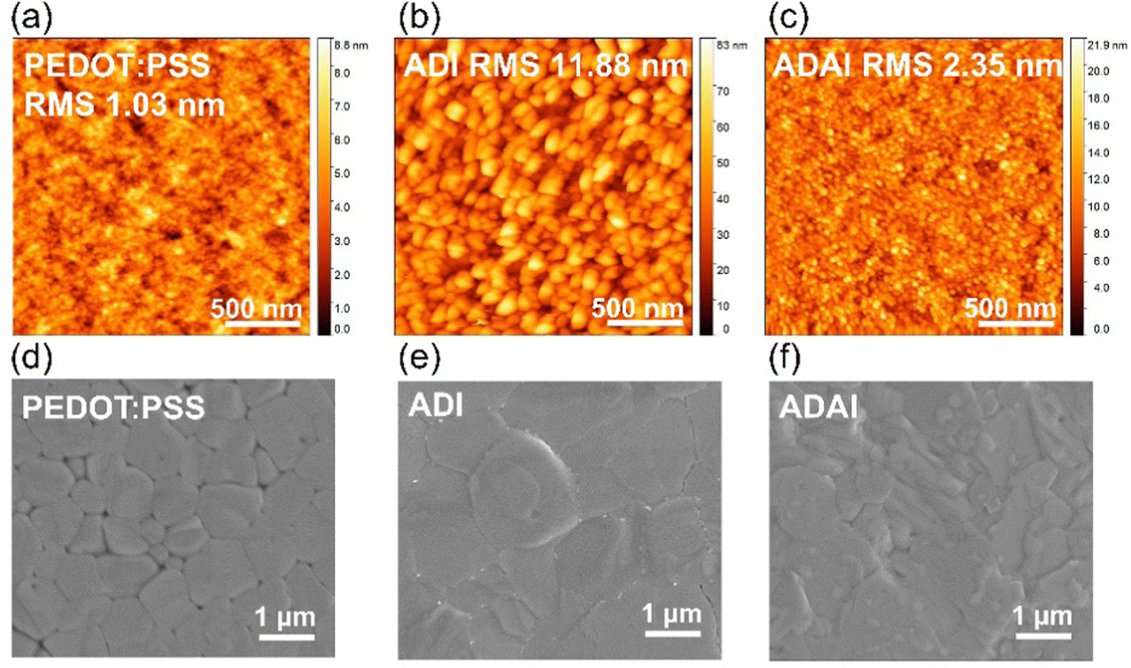 | ||
| Fig. 6 (a–c) Tapping mode 2 μm × 2 μm atomic force microscopy images of the indicated HTL on ITO; (d–f) Top-view scanning electron microscopy images of the perovskite layer coated on the indicated HTL. | ||
To better understand the charge transfer processes at the HTL/perovskite interface, steady-state photoluminescence (SSPL) experiments and time-resolved photoluminescence (TRPL) measurements were performed. The perovskite fluorescence was compared to that of the perovskite with the HTLs located underneath or atop to reproduce the deposition sequence of the layers used in the p–i–n and n–i–p configurations, respectively (Fig. 7). The presence of HTLs causes fluorescence quenching of the pristine perovskite, possibly because free holes generated upon exciting the perovskite layer are transferred to the HTL and contribute to a loss of radiative recombination.39 The larger quenching observed for ADAI is ascribed to its better robustness to the solution processing of the perovskite layer deposited on the HTL, due to the effect of the hydrogen bonded structure.28 This fact was also demonstrated acquiring the absorption spectra of the films of the HTLs before and after performing a DMF wash using the same deposition conditions as for the perovskite layer (Fig. S4, ESI‡). The ADAI film remained virtually unchanged whereas the ADI film was partially washed away. The effect of the deposition sequence is further evidenced by the larger quenching observed when the HTLs are deposited on the perovskite layer. Anyhow, these results show the better consistency in the performance of the self-assembled ADAI as HTL in the two configurations.
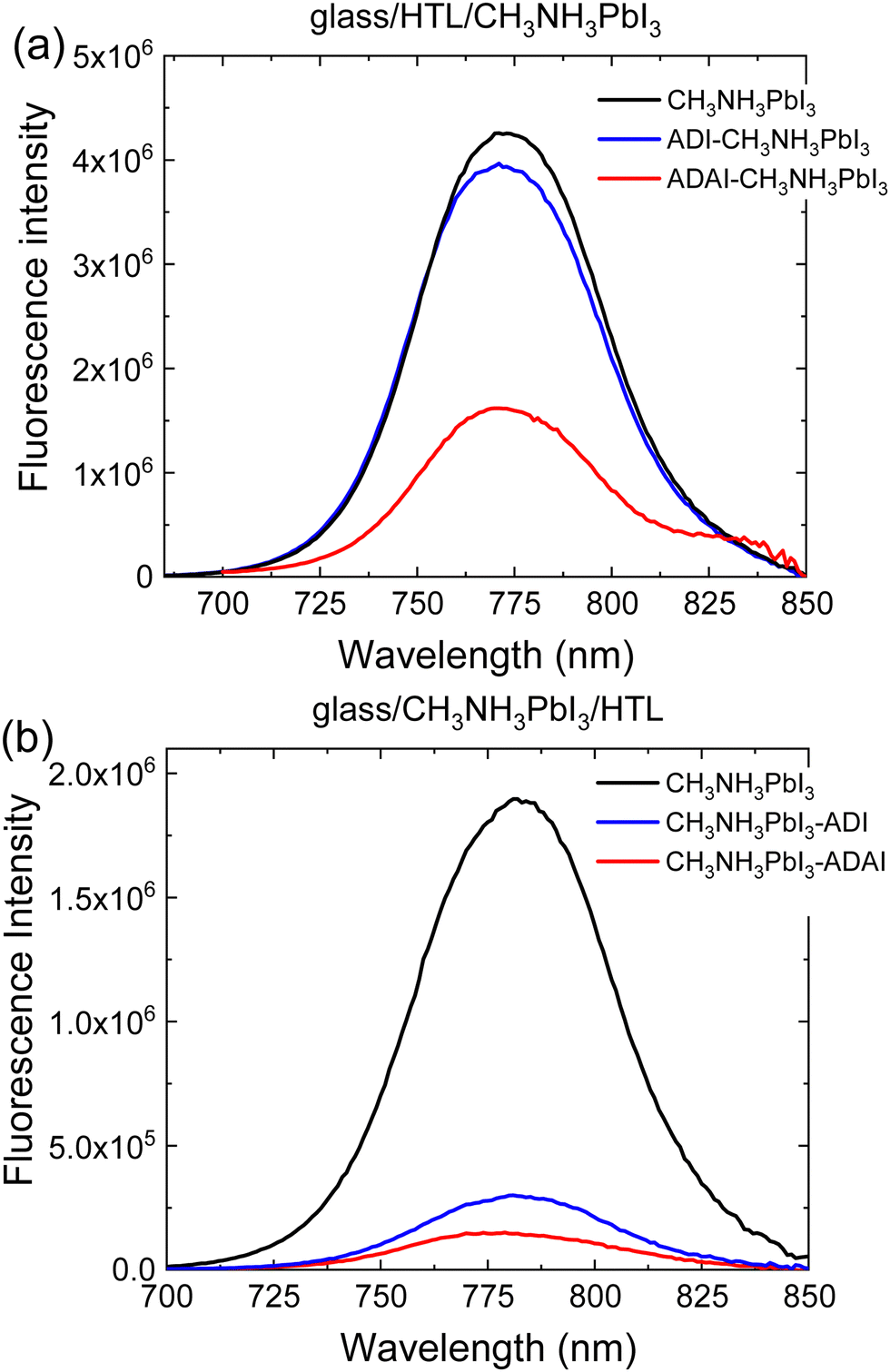 | ||
| Fig. 7 Photoluminescence spectra registered by excitation of the perovskite through the HTL interface. The relative position of the HTL with respect to the perovskite is indicated. | ||
The dynamics of the interfacial charge transfer were characterized by TRPL experiments using the time-correlated single photon counting (TCSPC) method. The photoluminescence decay was fitted to a bi-exponential model (Fig. S5, ESI‡). Concerning the two temporal regimes, the faster decay, τ1, is ascribed to charge transfer from the perovskite to the HTL and/or interface recombination, whereas the slower component, τ2, is attributed to bulk and/or surface recombination.40,41 When comparing to the pristine perovskite layer, a much shorter τ1 lifetimes (2–3 vs. 22 ns, Table S1, ESI‡) is detected in the presence of ADI or ADAI. This is consistent with the loss in PL intensity (Fig. 7) and interpreted as a fast charge transfer process from the perovskite to the HTL that reduces radiative recombination. The enhanced non-radiative recombination compared to the pristine layer will reduce the maximum attainable Voc, but as can be seen in Table 2 the Voc of the cells with ADAI is comparable to that obtained for the reference devices with p–i–n and n–i–p architectures using PEDOT:PSS or Spiro-MeOTAD as HTL. On the other hand, ADI provides a consistently lower Voc.
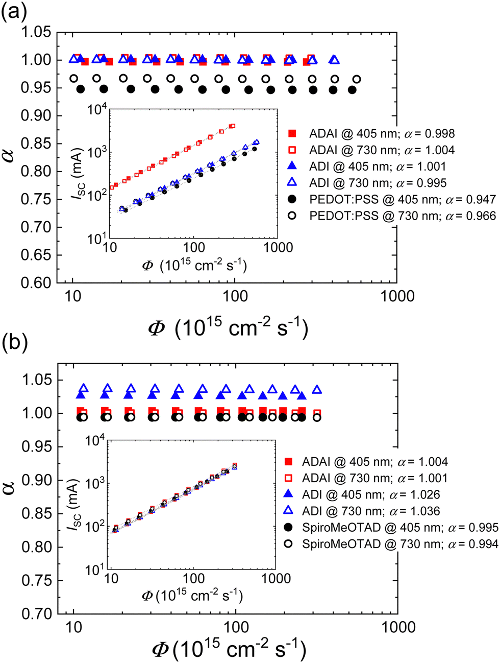
To further investigate the effect of the HTLs on the charge recombination mechanisms and its relationship with the performance of the solar cells, JSC and Voc were probed by increasing the intensity of the incident light. The experiments were performed by illuminating the devices with blue (λ = 405 nm) and red (λ = 730 nm) monochromatic LEDs.42 Because of lower absorption coefficient red light penetrates further into the active layer and provides results useful for the evaluation of recombination in the bulk of the perovskite layer. In contrast, blue light is mainly absorbed at the front perovskite/HTL (for p–i–n) or perovskite/ETL (for n–i–p) interface, which can be helpful to study the perovskite interfacial section. The dependence of JSC on the light intensity, expressed as photon flux (Φ), is modelled by the equation: JSC= CΦα, where C and α are constants.43,44 A double logarithmic representation shows a linear relationship between JSC and Φ (Fig. 8a and b inset) with the slope corresponding to α. Ideally, this exponent should have a value α ≈ 1, if bimolecular recombination of the photogenerated free charges and space-charge effects are not significantly affecting the performance of the solar cell.44,45 To better analyze the evolution of α with the light intensity, α values are assessed as α = log(JSC/C)/log![[thin space (1/6-em)]](https://www.rsc.org/images/entities/char_2009.gif) Φ and plotted as a function of logΦ (Fig. 8a and b). It is worth highlighting that the devices fabricated with ADAI and ADI present α very close to the ideal value which remains consistent with red and blue lights at different intensities, in either p–i–n or n–i–p architectures. These results indicate that the evaluated undoped materials can efficiently extract the photogenerated charges at short-circuit without a relevant contribution of bimolecular recombination pathways independently on their relative position with respect to the active layer. A similar behavior was observed for the doped Spiro-MeOTAD in n–i–p solar cells. Nevertheless, PEDOT:PSS-based p–i–n devices showed a more noticeable deviation from ideality (αred = 0.966; αblue = 0.947).
Φ and plotted as a function of logΦ (Fig. 8a and b). It is worth highlighting that the devices fabricated with ADAI and ADI present α very close to the ideal value which remains consistent with red and blue lights at different intensities, in either p–i–n or n–i–p architectures. These results indicate that the evaluated undoped materials can efficiently extract the photogenerated charges at short-circuit without a relevant contribution of bimolecular recombination pathways independently on their relative position with respect to the active layer. A similar behavior was observed for the doped Spiro-MeOTAD in n–i–p solar cells. Nevertheless, PEDOT:PSS-based p–i–n devices showed a more noticeable deviation from ideality (αred = 0.966; αblue = 0.947).
 | ||
| Fig. 8 Evolution of α and short-circuit current (inset) as a function of the photon flux (Φ) in devices with (a) p–i–n and (b) n–i–p configuration. | ||
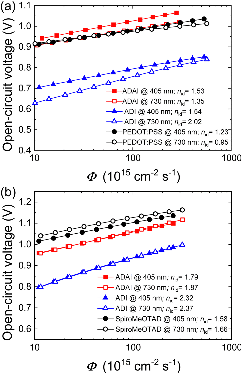
To analyze the recombination mechanisms at open circuit, the VOC was measured by increasing the incident light intensity (Fig. 9a and b). The VOC dependence on light intensity follows the equation 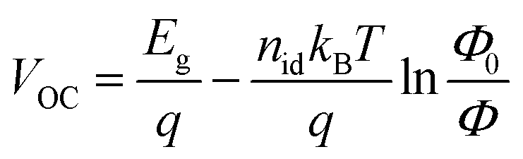 , where Eg corresponds to the bandgap, nid is the ideality factor, kB the Boltzmann constant, T the absolute temperature, and q the elementary charge. Generally, as a figure of merit, an ideality factor of 1 is related to a predominant band-to-band radiative recombination, whereas a value of 2 is associated to a larger impact of a trap-assisted Shockley–Read–Hall (SRH) recombination.46 The ideality factors extracted from the slope of the Vocvs. Φ plot in the higher intensity range are listed in the legends of Fig. 9a and b. Thus, regarding the devices with inverted configuration, the use of ADAI as HTL led to nid values that can be associated to the occurrence of combined recombination mechanisms with either blue or red illumination. In the case of ADI, a similar situation was detected with blue light. However, these devices exhibited a larger contribution of trap-assisted recombination, as it can be inferred from the nid value measured with red light, leading to a lower Voc.
 | ||
| Fig. 9 Semilogarithmic representation of the open-circuit voltage as a function of Φ in devices with (a) p–i–n and (b) n–i–p configuration. Light ideality factors are indicated in the legends. | ||
As far as the n–i–p devices are concerned, higher ideality factors are obtained for ADI and ADAI. This result is more pronounced in the case of ADI, showing a more evident effect of trap-assisted recombination (Fig. 9b). Conversely, undoped ADAI stays closer to the results obtained for the reference solar cell fabricated with doped Spiro-MeOTAD, whose nid values indicate that SRH recombination pathway seems to prevail, in combination with a band-to-band mechanism.47 The ideality factors do not strongly depend on the illumination wavelength. The fact that the ideality factors are consistently higher for ADI compared to ADAI, while the Voc is much less for ADI shows that ADAI reduces the effect of charge trapping in the recombination. Both in p–i–n and n–i–p devices, ADAI provides consistently higher Voc values. This shows again the versatility of this material as HTL in devices with conventional and inverted architectures.
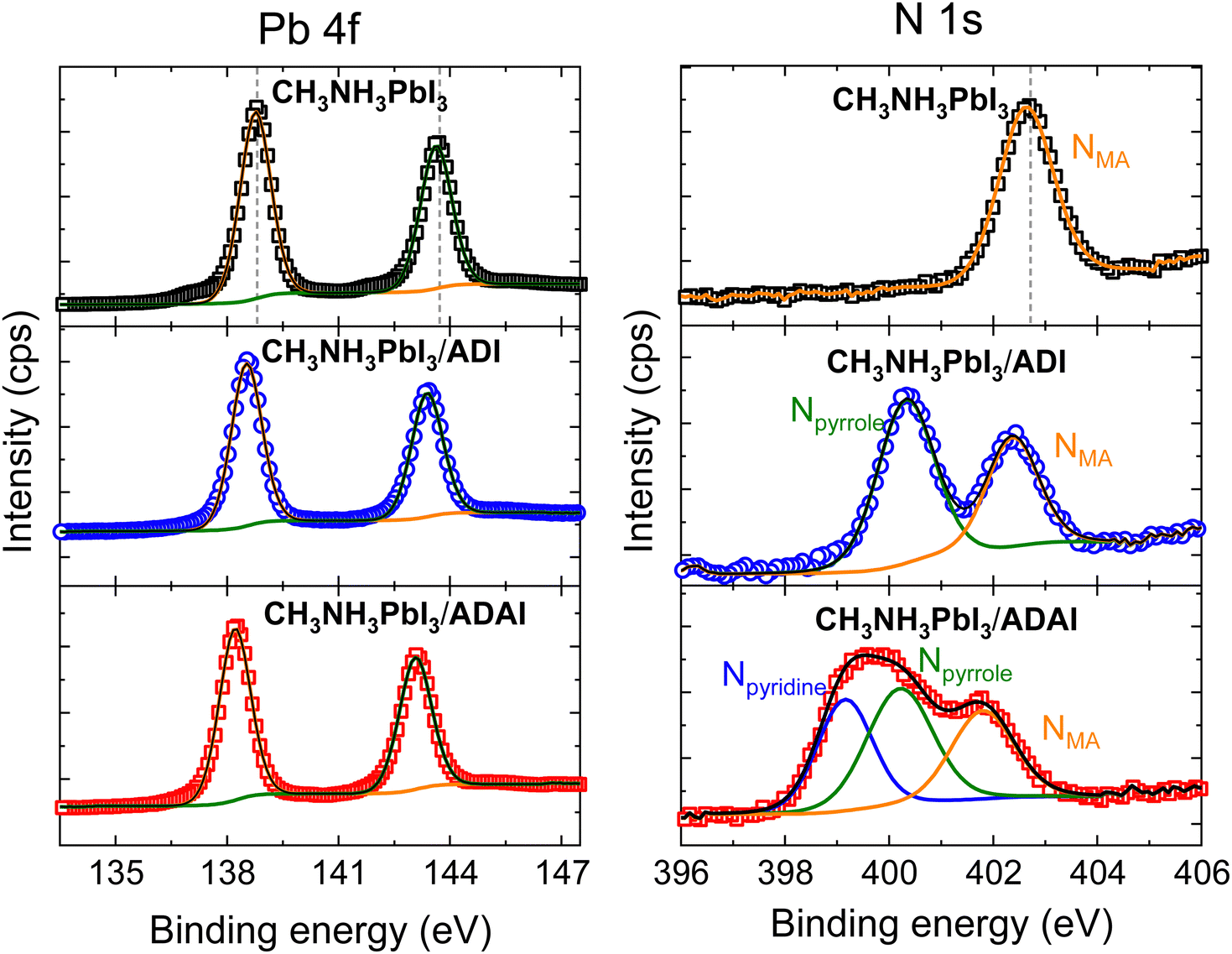
To identify the interactions taking place at the perovskite/HTL interface that can affect the solar cell performance, X-ray photoelectron spectroscopy (XPS) experiments were performed with perovskite samples covered by an ADI or ADAI layer (5 nm thick) deposited via thermal evaporation (Fig. 10). The XPS spectra of the Pb 4f core level of the perovskite comprises two symmetric peaks corresponding to the Pb 4f5/2 and Pb 4f7/2 levels located at binding energies (BE) of 138.8 eV and 143.7 eV, respectively.48 These peaks were shifted 0.3 eV and 0.6 eV towards lower BE values in the samples coated with ADI and ADAI, respectively. The larger shifts detected in the case of ADAI are indicative of stronger interactions.49 In this regard, the electron lone pair of the nitrogen atom in the pyridine rings of ADAI can interact with the lead cations, particularly those at the surface of the perovskite layer, with vacancies in their coordination sphere.50 The XPS spectra of the N 1s were also measured for the pristine perovskite, showing the peak of the methylammonium (MA) cation at 402.7 eV, and the perovskite/HTL bilayers. Two peaks were clearly resolved for the sample containing ADI, ascribed to the Npyrrole (400.3 eV) and the NMA (402.4 eV). The spectrum corresponding to the sample containing ADAI was deconvoluted to obtain the three expected peaks, namely Npyridine (399.2 eV), Npyrrole (400.3 eV) and NMA (401.8 eV). Whereas the possible interaction between the perovskite and the HTL is evidence by the shift of the NMA peak, it is also worth highlighting that the Npyridine peak is shifted to higher energies with respect to the BE reported for the pyridine (398.8 eV)51 indicating a coordinative interaction with the lead cations. These results additionally indicate the adequacy of the ADAI structure to work as interfacial layer and reinforce its versatility as HTL to be used in solar cells with conventional and inverted architecture.
 | ||
| Fig. 10 Pb 4f and N 1s core level XPS spectra of bare CH3NH3PbI3 and CH3NH3PbI3 coated with ADI and ADAI. | ||
Conclusions
In summary, it has been demonstrated that the rational design of polyheteroaromatic systems to promote hydrogen bond-directed self-assembly can become a suitable approach for the development of novel charge transporting materials. The particular structural features, based on the integration of 7-azaindole into the conjugated skeleton of ADAI, have led to the convergence of several properties that result in a versatile dual interfacial layer. Thus, hydrogen bonding bestows robustness to the material that admits the processing of adjacent films in different device architectures. Self-assembly also favours the nanostructuration of the material, its compatibility with an appropriate perovskite morphology and the improvement of the charge transport ability. Additionally, the presence of coordinating sites in the ADAI structure allows the defect passivation of undercoordinated lead cations at the surface of the perovskite layer, becoming an additional feature for improving its performance as dopant-free interfacial layer in p–i–n and n–i–p solar cells, and outperforming reference HTLs specific of each architecture.Conflicts of interest
There are no conflicts to declare.Acknowledgements
Authors acknowledge the financial support from the Ministry of Science and Innovation (PID2021-122734OB-I00; RED2022-134939-T), Fundación Séneca-Agencia de Ciencia y Tecnología de la Región de Murcia (Project 22058/PI/22).Notes and references
- M. Seri, F. Mercuri, G. Ruani, Y. Feng, M. Li, Z.-X. Xu and M. Muccini, Toward Real Setting Applications of Organic and Perovskite Solar Cells: A Comparative Review, Energy Technol., 2021, 9, 2000901 CrossRef CAS.
- J. J. Yoo, G. Seo, M. R. Chua, T. G. Park, Y. Lu, F. Rotermund, Y.-K. Kim, C. S. Moon, N. J. Jeon, J.-P. Correa-Baena, V. Bulović, S. S. Shin, M. G. Bawendi and J. Seo, Efficient perovskite solar cells via improved carrier management, Nature, 2021, 590, 587–593 CrossRef CAS PubMed.
- M. A. Green, E. D. Dunlop, G. Siefer, M. Yoshita, N. Kopidakis, K. Bothe and X. Hao, Solar cell efficiency tables (Version 61), Prog. Photovolt: Res. Appl., 2023, 31, 3–16 CrossRef.
- T. Wang, W. Deng, J. Cao and F. Yan, Recent Progress on Heterojunction Engineering in Perovskite Solar Cells, Adv. Energy Mater., 2022, 2201436 CrossRef.
- M. Jeong, I. W. Choi, E. M. Go, Y. Cho, M. Kim, B. Lee, S. Jeong, Y. Jo, H. W. Choi, J. Lee, J.-H. Bae, S. K. Kwak, D. S. Kim and C. Yang, Stable perovskite solar cells with efficiency exceeding 24.8% and 0.3-V voltage loss, Science, 2020, 369, 1615–1620 CrossRef CAS PubMed.
- J. Peng, D. Walter, Y. Ren, M. Tebyetekerwa, Y. Wu, T. Duong, Q. Lin, J. Li, T. Lu, M. A. Mahmud, O. L. C. Lem, S. Zhao, W. Liu, Y. Liu, H. Shen, L. Li, F. Kremer, H. T. Nguyen, D.-Y. Choi, K. J. Weber, K. R. Catchpole and T. P. White, Nanoscale localized contacts for high fill factors in polymer-passivated perovskite solar cells, Science, 2021, 371, 390–395 CrossRef CAS PubMed.
- Z. Li, B. Li, X. Wu, S. A. Sheppard, S. Zhang, D. Gao, N. J. Long and Z. Zhu, Organometallic-functionalized interfaces for highly efficient inverted perovskite solar cells, Science, 2022, 376, 416–420 CrossRef CAS PubMed.
- X. Zheng, Y. Hou, C. Bao, J. Yin, F. Yuan, Z. Huang, K. Song, J. Liu, J. Troughton, N. Gasparini, C. Zhou, Y. Lin, D.-J. Xue, B. Chen, A. K. Johnston, N. Wei, M. N. Hedhili, M. Wei, A. Y. Alsalloum, P. Maity, B. Turedi, C. Yang, D. Baran, T. D. Anthopoulos, Y. Han, Z.-H. Lu, O. F. Mohammed, F. Gao, E. H. Sargent and O. M. Bakr, Managing grains and interfaces via ligand anchoring enables 22.3%-efficiency inverted perovskite solar cells, Nat. Energy, 2020, 5, 131–140 CrossRef CAS.
- S. Shao and M. A. Loi, The Role of the Interfaces in Perovskite Solar Cells, Adv. Mater. Interf., 2020, 7, 1901469 CrossRef CAS.
- H. Xu, F. Yuan, D. Zhou, X. Liao, L. Chen and Y. Chen, Hole transport layers for organic solar cells: recent progress and prospects, J. Mater. Chem. A, 2020, 8, 11478–11492 RSC.
- X. Yang, H. Wang, B. Cai, Z. Yu and L. Sun, Progress in hole-transporting materials for perovskite solar cells, J. Energy Chem., 2018, 27, 650–672 CrossRef.
- Q. Wang, Z. Lin, J. Su, Z. Hu, J. Chang and Y. Hao, Recent progress of inorganic hole transport materials for efficient and stable perovskite solar cells, Nano Select, 2021, 2, 1055–1080 CrossRef CAS.
- Z. Yu and L. Sun, Inorganic Hole-Transporting Materials for Perovskite Solar Cells, Small Methods, 2018, 2, 1700280 CrossRef.
- M. Vasilopoulou, A. Fakharuddin, A. G. Coutsolelos, P. Falaras, P. Argitis, A. R. B. M. Yusoff and M. K. Nazeeruddin, Molecular materials as interfacial layers and additives in perovskite solar cells, Chem. Soc. Rev., 2020, 49, 4496–4526 RSC.
- X. Zhao and M. Wang, Organic hole-transporting materials for efficient perovskite solar cells, Mater. Today Energy, 2018, 7, 208–220 CrossRef.
- Z. Wenxiao, W. Ying-Chiao, L. Xiaodong, S. Changjian, W. Li, U. Khurram and F. Junfeng, Recent Advance in Solution-Processed Organic Interlayers for High-Performance Planar Perovskite Solar Cells, Adv. Sci., 2018, 5, 1800159 CrossRef.
- Y. Yao, C. Cheng, C. Zhang, H. Hu, K. Wang and S. De Wolf, Organic Hole-Transport Layers for Efficient, Stable, and Scalable Inverted Perovskite Solar Cells, Adv. Mater., 2022, 34, 2203794 CrossRef CAS PubMed.
- S. Y. Kim, S. J. Cho, S. E. Byeon, X. He and H. J. Yoon, Self-Assembled Monolayers as Interface Engineering Nanomaterials in Perovskite Solar Cells, Adv. Energy Mater., 2020, 10, 2002606 CrossRef CAS.
- K. Choi, H. Choi, J. Min, T. Kim, D. Kim, S. Y. Son, G.-W. Kim, J. Choi and T. Park, A Short Review on Interface Engineering of Perovskite Solar Cells: A Self-Assembled Monolayer and Its Roles, Solar RRL, 2020, 4, 1900251 CrossRef.
- F. Ali, C. Roldán-Carmona, M. Sohail and M. K. Nazeeruddin, Applications of Self-Assembled Monolayers for Perovskite Solar Cells Interface Engineering to Address Efficiency and Stability, Adv. Energy Mater., 2020, 10, 2002989 CrossRef CAS.
- P. Yan, D. Yang, H. Wang, S. Yang and Z. Ge, Recent advances in dopant-free organic hole-transporting materials for efficient, stable and low-cost perovskite solar cells, Energy Environ. Sci., 2022, 15, 3630–3669 RSC.
- H. D. Pham, T. C.-J. Yang, S. M. Jain, G. J. Wilson and P. Sonar, Development of Dopant-Free Organic Hole Transporting Materials for Perovskite Solar Cells, Adv. Energy Mater., 2020, 10, 1903326 CrossRef CAS.
- W. Zhou, Z. Wen and P. Gao, Less is More: Dopant-Free Hole Transporting Materials for High-Efficiency Perovskite Solar Cells, Adv. Energy Mater., 2018, 8, 1702512 CrossRef.
- E. Rezaee, X. Liu, Q. Hu, L. Dong, Q. Chen, J.-H. Pan and Z.-X. Xu, Dopant-Free Hole Transporting Materials for Perovskite Solar Cells, Solar RRL, 2018, 2, 1800200 CrossRef.
- R. Grisorio, R. Iacobellis, A. Listorti, L. De Marco, M. P. Cipolla, M. Manca, A. Rizzo, A. Abate, G. Gigli and G. P. Suranna, Rational Design of Molecular Hole-Transporting Materials for Perovskite Solar Cells: Direct versus Inverted Device Configurations, ACS Appl. Mater. Interfaces, 2017, 9, 24778–24787 CrossRef CAS PubMed.
- X. Sun, Q. Xue, Z. Zhu, Q. Xiao, K. Jiang, H.-L. Yip, H. Yan and Z. A. Li, Fluoranthene-based dopant-free hole transporting materials for efficient perovskite solar cells, Chem. Sci., 2018, 9, 2698–2704 RSC.
- P. Gómez, S. Georgakopoulos, M. Más-Montoya, J. Cerdá, J. Pérez, E. Ortí, J. Aragó and D. Curiel, Improving the Robustness of Organic Semiconductors through Hydrogen Bonding, ACS Appl. Mater. Interfaces, 2021, 13, 8620–8630 CrossRef PubMed.
- P. Gómez, J. Wang, M. Más-Montoya, D. Bautista, C. H. L. Weijtens, D. Curiel and R. A. J. Janssen, Pyrene-Based Small-Molecular Hole Transport Layers for Efficient and Stable Narrow-Bandgap Perovskite Solar Cells, Solar RRL, 2021, 5, 2100454 CrossRef.
- M. Más-Montoya, P. Gómez, D. Curiel, I. da Silva, J. Wang and R. A. J. Janssen, A Self-Assembled Small-Molecule-Based Hole-Transporting Material for Inverted Perovskite Solar Cells, Chem. – Eur. J., 2020, 26, 10276–10282 CrossRef PubMed.
- N. Nijegorodov, V. Ramachandran and D. P. Winkoun, The dependence of the absorption and fluorescence parameters, the intersystem crossing and internal conversion rate constants on the number of rings in polyacene molecules, Spectrochim. Acta, Part A, 1997, 53, 1813–1824 CrossRef.
- N. J. Hestand, H. Yamagata, B. Xu, D. Sun, Y. Zhong, A. R. Harutyunyan, G. Chen, H.-L. Dai, Y. Rao and F. C. Spano, Polarized Absorption in Crystalline Pentacene: Theory vs Experiment, J. Phys. Chem. C, 2015, 119, 22137–22147 CrossRef CAS.
- F. C. Spano, The Spectral Signatures of Frenkel Polarons in H- and J-Aggregates, Acc. Chem. Res., 2010, 43, 429–439 CrossRef CAS PubMed.
- P. N. Murgatroyd, Theory of space-charge-limited current enhanced by Frenkel effect, J. Phys. D: Appl. Phys., 1970, 3, 151–156 CrossRef.
- R. S. Sanchez, V. Gonzalez-Pedro, J.-W. Lee, N.-G. Park, Y. S. Kang, I. Mora-Sero and J. Bisquert, Slow Dynamic Processes in Lead Halide Perovskite Solar Cells. Characteristic Times and Hysteresis, J. Phys. Chem. Lett., 2014, 5, 2357–2363 CrossRef CAS PubMed.
- W. Chen, D.-C. Qi, H. Huang, X. Gao and A. T. S. Wee, Organic–Organic Heterojunction Interfaces: Effect of Molecular Orientation, Adv. Funct. Mater., 2011, 21, 410–424 CrossRef CAS.
- G. J. Simpson and K. L. Rowlen, Molecular Orientation at Surfaces: Surface Roughness Contributions to Measurements Based on Linear Dichroism, J. Phys. Chem. B, 1999, 103, 3800–3811 CrossRef CAS.
- O. Almora, D. Baran, G. C. Bazan, C. Berger, C. I. Cabrera, K. R. Catchpole, S. Erten-Ela, F. Guo, J. Hauch, A. W. Y. Ho-Baillie, T. J. Jacobsson, R. A. J. Janssen, T. Kirchartz, N. Kopidakis, Y. Li, M. A. Loi, R. R. Lunt, X. Mathew, M. D. McGehee, J. Min, D. B. Mitzi, M. K. Nazeeruddin, J. Nelson, A. F. Nogueira, U. W. Paetzold, N.-G. Park, B. P. Rand, U. Rau, H. J. Snaith, E. Unger, L. Vaillant-Roca, H.-L. Yip and C. J. Brabec, Device Performance of Emerging Photovoltaic Materials (Version 2), Adv. Energy Mater., 2021, 11, 2102526 CrossRef CAS.
- A.-F. Castro-Méndez, J. Hidalgo and J.-P. Correa-Baena, The Role of Grain Boundaries in Perovskite Solar Cells, Adv. Energy Mater., 2019, 9, 1901489 CrossRef.
- J. J. van Franeker, K. H. Hendriks, B. J. Bruijnaers, M. W. G. M. Verhoeven, M. M. Wienk and R. A. J. Janssen, Monitoring Thermal Annealing of Perovskite Solar Cells with In Situ Photoluminescence, Adv. Energy Mater., 2017, 7, 1601822 CrossRef.
- M. Stolterfoht, C. M. Wolff, J. A. Márquez, S. Zhang, C. J. Hages, D. Rothhardt, S. Albrecht, P. L. Burn, P. Meredith, T. Unold and D. Neher, Visualization and suppression of interfacial recombination for high-efficiency large-area pin perovskite solar cells, Nat. Energy, 2018, 3, 847–854 CrossRef CAS.
- Q. Cao, Y. Li, H. Zhang, J. Yang, J. Han, T. Xu, S. Wang, Z. Wang, B. Gao, J. Zhao, X. Li, X. Ma, S. M. Zakeeruddin, W. E. I. Sha, X. Li and M. Grätzel, Efficient and stable inverted perovskite solar cells with very high fill factors via incorporation of star-shaped polymer, Sci. Adv., 2021, 7, eabg0633 CrossRef CAS PubMed.
- J.-P. Correa-Baena, W. Tress, K. Domanski, E. H. Anaraki, S.-H. Turren-Cruz, B. Roose, P. P. Boix, M. Grätzel, M. Saliba, A. Abate and A. Hagfeldt, Identifying and suppressing interfacial recombination to achieve high open-circuit voltage in perovskite solar cells, Energy Environ. Sci., 2017, 10, 1207–1212 RSC.
- P. Hartnagel and T. Kirchartz, Understanding the Light-Intensity Dependence of the Short-Circuit Current of Organic Solar Cells, Adv. Theory Simul., 2020, 3, 2000116 CrossRef CAS.
- L. J. A. Koster, V. D. Mihailetchi, H. Xie and P. W. M. Blom, Origin of the light intensity dependence of the short-circuit current of polymer/fullerene solar cells, Appl. Phys. Lett., 2005, 87, 203502 CrossRef.
- V. D. Mihailetchi, J. Wildeman and P. W. M. Blom, Space-Charge Limited Photocurrent, Phys. Rev. Lett., 2005, 94, 126602 CrossRef CAS PubMed.
- W. Tress, M. Yavari, K. Domanski, P. Yadav, B. Niesen, J. P. Correa Baena, A. Hagfeldt and M. Graetzel, Interpretation and evolution of open-circuit voltage, recombination, ideality factor and subgap defect states during reversible light-soaking and irreversible degradation of perovskite solar cells, Energy Environ. Sci., 2018, 11, 151–165 RSC.
- N. Thongprong, T. Supasai, Y. Li, I.-M. Tang and N. Rujisamphan, Insights into Recombination Processes from Light Intensity–Dependent Open-Circuit Voltages and Ideality Factors in Planar Perovskite Solar Cells, Energy Technol., 2020, 8, 1901196 CrossRef CAS.
- S. Béchu, M. Ralaiarisoa, A. Etcheberry and P. Schulz, Photoemission Spectroscopy Characterization of Halide Perovskites, Adv. Energy Mater., 2020, 10, 1904007 CrossRef.
- S. Y. Kim, H. Kang, K. Chang and H. J. Yoon, Case Studies on Structure–Property Relations in Perovskite Light-Emitting Diodes via Interfacial Engineering with Self-Assembled Monolayers, ACS Appl. Mater. Interfaces, 2021, 13, 31236–31247 CrossRef CAS PubMed.
- H.-R. Liu, S.-H. Li, L.-L. Deng, Z.-Y. Wang, Z. Xing, X. Rong, H.-R. Tian, X. Li, S.-Y. Xie, R.-B. Huang and L.-S. Zheng, Pyridine-Functionalized Fullerene Electron Transport Layer for Efficient Planar Perovskite Solar Cells, ACS Appl. Mater. Interfaces, 2019, 11, 23982–23989 CrossRef CAS PubMed.
- K. Artyushkova, Misconceptions in interpretation of nitrogen chemistry from X-ray photoelectron spectra, J. Vac. Sci. Technol., A, 2020, 38, 031002 CrossRef CAS.
Footnotes |
| † Dedicated to Professor Alberto Tárraga on the occasion of his 70th birthday. |
| ‡ Electronic supplementary information (ESI) available. See DOI: https://doi.org/10.1039/d3qm00425b |
| This journal is © the Partner Organisations 2023 |