
 Open Access Article
 This Open Access Article is licensed under a Creative Commons Attribution-Non Commercial 3.0 Unported Licence
Electronic properties of single Prussian Blue Analog nanocrystals determined by conductive-AFM†
Hugo
Therssen
a,
Laure
Catala
 b,
Sandra
Mazérat
b,
Talal
Mallah
b,
Dominique
Vuillaume
a,
Thierry
Mélin
a and
Stéphane
Lenfant
*a
b,
Sandra
Mazérat
b,
Talal
Mallah
b,
Dominique
Vuillaume
a,
Thierry
Mélin
a and
Stéphane
Lenfant
*a
aUniv. Lille, CNRS, Univ. Polytechnique Hauts-de-France, UMR 8520 – IEMN – Institut d'Electronique de Microélectronique et de Nanotechnologie, F-59000 Lille, France. E-mail: stephane.lenfant@iemn.fr
bInstitut de Chimie Moléculaire et des Matériaux d'Orsay (ICMMO), CNRS, Université Paris-Saclay, 91400 Orsay Cedex, France
First published on 31st October 2023
Abstract
We report a study of the electron transport (ET) properties at the nanoscale (conductive-AFM denoted as C-AFM hereafter) of individual Prussian Blue Analog (PBA) cubic nanocrystals (NCs) of CsCoIIIFeII, with a size between 15 and 50 nm deposited on HOPG. We demonstrate that these PBA NCs feature an almost size-independent electron injection barrier of 0.41 ± 0.02 eV and 0.27 ± 0.03 eV at the CsCoIIIFeII/HOPG and CsCoIIIFeII/C-AFM tip, respectively, and an intrinsic electron conductivity evolving from a large dispersion between ∼5 × 10⁻⁴ and 2 × 10⁻² S cm−1 without a clear correlation with the nanocrystal size. The conductivity values measured on individual nanocrystals are up to fifty times higher than those reported on PBA films.
Introduction
Prussian Blue Analog (PBA) nanocrystals are nano-objects at the frontier between molecules and bulk materials and have molecular properties that can be used for different applications1,2 such as gas storage3–5 materials for energy issues,6–9 magnetic properties for information storage,10 electrochemical and biosensors,11 catalysis,12 environmental purification,13,14 or biomedical applications.15 The structure of a PBA consists of a cyanide-bridged bimetallic face-centered cubic (fcc) arrangement obtained from the reaction of a hexametallocyanate (negatively charged) and a hexa-aquometallate of transition metal ions (Fe in the pristine Prussian Blue) upon substitution of water molecules by the nitrogen atoms of the metallocyanate molecules.16 The neutrality of the network is ensured either by the presence of metallocyanate vacancies and/or by the insertion of positively charged alkali ions in the tetrahedral sites of the fcc structure. A wide variety of PBAs have been synthesized using different transition metal ions such as Cr, Mn, and Co.17,18 At the nanoscale, nanocrystals were prepared in water allowing the stabilization of nanocrystals with a well-defined size and shape,19 and this led using a seed-mediated approach to the design of core–multishell heterostructures.20 The same approach is used here to prepare nanocrystals of increased size.Here, we present a study of the electronic transport (ET) through isolated PBA nanocrystals composed of Cs{CoIII[FeII(CN)6]} denoted as CsCoFe hereafter. Only a few results exist in the literature, describing the ET properties of PBA. In particular, the electron injection energy barriers at the contact interface and the intrinsic conductivity of PBA NCs have not been investigated so far. Previous experiments consisted in either ET experiments conducted at the microscale on film or powders21–23 or results obtained by our group at the nanoscale24 demonstrating a weak attenuation of the electron transport through several (up to 3) CsCoFe NCs (15 nm in size) connected in series between two electrodes, i.e. a low electron transfer decay factor β = 0.11 nm−1, with the current I ∝ e−βd, where d is the distance between the electrodes (15 < d < 45 nm). The current decay in these multi-NC devices was ascribed to a multi-step coherent tunneling between adjacent NCs with a strong energy coupling (0.1–0.25 eV) between the adjacent CsCoFe NCs.24 Here, we report ET in individual CsCoFe NCs of various sizes in the same range (nominally: 15 nm, 30 nm and 50 nm). We prepared and deposited CsCoFe NCs on highly ordered pyrolytic graphite (HOPG) surfaces and we characterized the electronic transport through individual NCs, i.e. in HOPG/single PBA/C-AFM tip devices as a function of the PBA NC size (Fig. 1). We found that the current increases with the NC size. To analyze the experimental current–voltage curves, we used two models. We first considered a quantum transport model as in our previous study of ET in one to three 15 nm NCs in series.24 In this single energy level (SEL) model,25,26 the electrons are transferred between the two electrodes through a single molecular orbital (MO). Since the NC size is large compared to atomic and molecular scales (for which the SEL model was initially developed), we have also used a model suitable for nanoscale devices, i.e. a nano-Schottky diode as already used for C-AFM-tip/semiconductor nanocrystals, quantum dots and nanostructure interfaces.27–29 More specifically, we used a simple analytical model that consists of a double Schottky barrier (DSB) model30 (one Schottky diode at each interface) in series with the intrinsic resistance of the PBA NCs. The main observed features are the following:
(i) The SEL model gives an energy level of the MO involved in the ET at about 0.3–0.5 eV below the Fermi energy of the electrodes, independent of the NC size, in agreement with the values in ref. 24.
(ii) The increase of the current with the NC size is not well explained by this model.
(iii) With the DSB model, we found a Schottky barrier height (SBH) for a hole injection of 0.41 ± 0.02 eV at the CsCoFe/HOPG interface and 0.27 ± 0.03 eV at the CsCoFe/C-AFM PtIr tip, independent of the NC size. This finding is in contrast to that of a size-dependent SBH observed in various non-ideal Schottky diodes,31–33 or diodes with nanometer-scale contacts,34,35 and nano-diodes made of semiconducting nanocrystals or nanodots.27–29
(iv) The intrinsic electron conductivity of the CsCoFe NCs is largely dispersed between ∼5 × 10⁻⁴ S cm−1 and 2 × 10⁻² S cm−1 without a correlation with the NC size.
 | ||
| Fig. 1 (a) Scheme of a unit cell of the fcc structure of CsCoFe PBA NCs (adapted from ref. 24). The cell parameter is close to 10 Å. (b) Scheme of the conducting AFM experiments, in which an individual PBA NC with a characteristic size of around 50 nm deposited on a freshly cleaved HOPG substrate is addressed, and statistics of I(V) characteristics are recorded using a given AFM tip force (see text). The AFM PtIr coated tip is grounded, and the voltage V is applied on the HOPG substrate. | ||
Experimental section
Sample preparation
The synthesis of the 15 nm CsCoFe nanocrystals has been reported elsewhere.24,36 The larger size objects were obtained by the same approach used for similar CsNiCr NCs (see details in the ESI, section 1†).37 The CsCoFe NCs are then deposited on a HOPG substrate by immersing a freshly cleaved HOPG surface in the colloidal suspension for 20 seconds. This step is followed by a thorough rinsing of the sample with deionized water and then with methanol and finally a drying step under vacuum for several hours. The samples appeared stable over time in ambient air and at room temperature but have nevertheless been kept in a nitrogen environment for storage purposes.C-AFM measurements were realized in an air-conditioned laboratory (Tamb = 22.5 °C, a relative humidity of 35–40%), with a Dimension Icon microscope (Brüker, US) equipped with a Nanoscope V controller and a PF-TUNA module with sensitivity factors comprised between 20 pA V−1 and 100 nA V−1. Conductive (PtIr metal plated) tips have been used, both for topography imaging and I(V) measurements (SCM-PIT-V2 from Brüker with an apex radius of ∼25 nm, a spring constant k = 2.8 N m−1, and a resonance frequency of 75 kHz). Contact-mode AFM was not used for sample imaging since it leads to the displacement of NCs outside the scanning area, even using a low scanning force (a few nN), due to the weak interaction force between the PBA NCs and the substrate. We instead imaged the sample topography in tapping mode and addressed individual NCs electrically by switching from tapping to contact mode with the tip almost in point mode above a given NC. More precisely, the measurement procedure is conducted as follows: (i) the sample topography is acquired in tapping mode (TM-AFM); (ii) an isolated PBA NC is selected; (iii) the TM-AFM scan is progressively focused on the NC top (final scan size below 10 × 10 nm2); (iv) the AFM oscillation driving amplitude is suppressed to stop the cantilever oscillation; (v) the AFM tip is then gently brought into contact with the NC top, while monitoring the applied force as from the cantilever static deflection; (vi) I(V) characteristics are recorded using a typical tip force of 15 nN (experimental data consist of a set of about 100–400 I(V) curves successively obtained by applying voltage ramps between −1 V and +1 V in the forward and then backward direction). All the I–V curves were acquired with the C-AFM tip positioned on the top surface of the PBA NC; (vii) after the I(V) data acquisition, the sample topography is imaged back in tapping mode to check for the integrity of the individual NC. For a given NC size, 2 to 3 NCs were measured on the same sample using the above-described I(V) measurement scheme.
Results
Topography by AFM after the NC layer deposition
Typical TM-AFM and scanning electron microscopy (SEM) images of CsCoFe NCs of different sizes freshly deposited on HOPG substrates from a colloidal solution are presented in Fig. 2. TM-AFM images confirmed the presence of NCs on the HOPG substrates with a sub-monolayer coverage. The surface coverage, however, differs from sample to sample (due to the simplistic deposition method). Samples with 15 nm NCs have a surface coverage of ca. ∼220 NCs per μm2, and the histogram/grain size analysis, shown in Fig. 2b, showed an average NC size of 15.8 ± 4.9 nm. The surface with 30 nm NCs presents a lower surface coverage of around 57 NCs per μm2, with an average NC height of 26.9 ± 7.2 nm and for the 50 nm NCs, we obtained ca. ∼110 NCs per μm2 and an average NC height of 42.4 ± 18.1 nm. We notice a clear increase in the dispersion of the NC size with the increase of the nominal size of the NCs, and this is due to the multistep synthetic method used to prepare nanocrystals with increased size (see the ESI† for details). All samples (with nominal NC sizes of 15 nm, 30 nm and 50 nm) on HOPG substrates enabled access of individual NCs, as seen from the AFM images (and cross-sections) shown in Fig. 2d and e. Accessing individual NCs in a controlled way is a prerequisite to conducting ET measurements. In Fig. 2d, isolated nanocrystals of 15 nm, 30 nm and 50 nm of CsCoFe are presented with their corresponding height profiles. We find the nominal height for each nanocrystal with, however, a larger lateral size due to the convolution effect with the radius of curvature of the AFM tip (estimated by the supplier around 25 nm).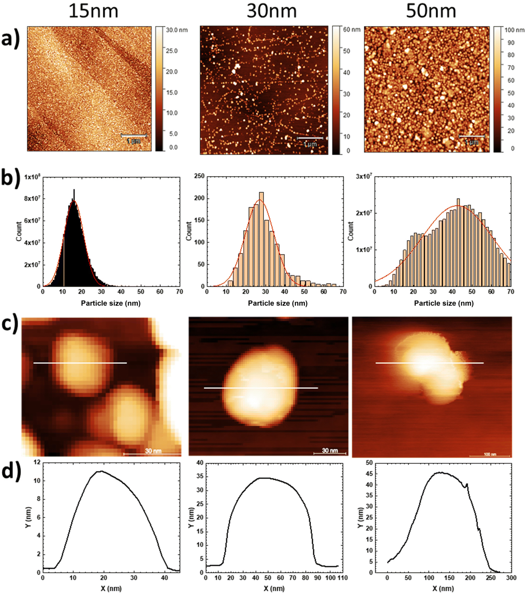 | ||
| Fig. 2 (a) 5 × 5 μm topographic TM-AFM images for the three sizes of CsCoFe NCs (15 nm, 30 nm and 50 nm) deposited on a HOPG substrate. (b) Corresponding height histograms (function Statistical Functions/Distribution of heights in Gwyddion v2.60 software) (15 nm and 50 nm NCs). Histograms for the 30 nm NCs have been obtained using a grain recognition analysis (function Data Process/Grains/Mark by Edge Detection with a Laplacian fixed at 55% in Gwyddion v2.60 software) due to the lower NC surface coverage. The average heights and the standard deviations have been obtained from the fit of the histogram with a Gaussian distribution (red lines). (c) TM-AFM images of single NCs with (d) the corresponding cross sections. | ||
Electronic transport properties by C-AFM
Fig. 3 illustrates the evolution of current–voltage I(V) characteristics of NCs as a function of their size. For each size of CsCoFe NC, the current–voltage I(V) 2D histograms (Fig. 3, middle) reveal low dispersed current values. The current histograms at a fixed voltage (here ±0.4 V) are fitted with a log–normal distribution given a log-mean current (log![[thin space (1/6-em)]](https://www.rsc.org/images/entities/char_2009.gif) Ī) and a log-standard deviation (logσ). We note a low logσ (lower than 0.3, see Table 1) indicating a reproducible and controlled acquisition of the I(V) characteristics with the C-AFM. By comparison, the I(V) 2D histogram realized on the same HOPG substrate (as a reference) presents higher current levels (e.g. logĪ > −8.5, Ī > 3 × 10⁻⁹ A, at 0.4 V) (see Fig. S2 in the ESI†), and thus the I(V) characteristics shown in Fig. 3 correspond to the ET properties through the PBA NCs. The I(V) curves on NCs appear almost symmetric, with low ratios (less than 3 measured at ±1 V). The same measurements were done for other NCs deposited on the same HOPG samples; the corresponding datasets are shown in section 3 in the ESI, Fig. S3†. Fig. 4 summarizes the evolution of the mean current Ī (at ±1 V for all the measured samples).
Ī) and a log-standard deviation (logσ). We note a low logσ (lower than 0.3, see Table 1) indicating a reproducible and controlled acquisition of the I(V) characteristics with the C-AFM. By comparison, the I(V) 2D histogram realized on the same HOPG substrate (as a reference) presents higher current levels (e.g. logĪ > −8.5, Ī > 3 × 10⁻⁹ A, at 0.4 V) (see Fig. S2 in the ESI†), and thus the I(V) characteristics shown in Fig. 3 correspond to the ET properties through the PBA NCs. The I(V) curves on NCs appear almost symmetric, with low ratios (less than 3 measured at ±1 V). The same measurements were done for other NCs deposited on the same HOPG samples; the corresponding datasets are shown in section 3 in the ESI, Fig. S3†. Fig. 4 summarizes the evolution of the mean current Ī (at ±1 V for all the measured samples).
 | ||
| Fig. 3 C-AFM 2D current–voltage I(V) histograms obtained with around 200 IV traces (middle) and the corresponding 1D histograms at −0.4 V (left) and +0.4 V (right) for three NCs of 15 nm, 30 nm and 50 nm deposited on bare clean HOPG (dataset #1). The average current at +/−0.4 V (logĪ) and the log-standard deviation (logσ) were obtained on each 1D histogram from the fit with a Gaussian distribution (red lines), see fitted values in Table 1. | ||
 | ||
| Fig. 4 Mean current at 1 V (filled symbol) and −1 V (open symbol) for all the measured dataset: for data shown in Fig. 3 (black square symbols), dataset #2 in Fig. S3† (red circle symbols), and dataset #3 in Fig. S3† (blue triangle symbols). | ||
Ī), the corresponding mean current Ī, and the log-standard deviation (logσ)
| 15 nm NC | 30 nm NC | 50 nm NC | ||
|---|---|---|---|---|
| −0.4 V | logĪ |
−10.73 | −10.35 | −9.31 |
| Ī (A) | 1.86 × 10⁻¹¹ | 4.47 × 10⁻¹¹ | 4.90 × 10⁻¹⁰ | |
| logσ |
0.18 | 0.23 | 0.26 | |
| +0.4 V | log-Ī | −10.76 | −10.76 | −9.51 |
| Ī (A) | 1.74 × 10⁻¹¹ | 1.74 × 10⁻¹¹ | 3.09 × 10⁻¹⁰ | |
| logσ |
0.25 | 0.15 | 0.25 |
Discussion
Fig. 3 and 4 show that the current increases with the NC size increasing from 15 nm to 50 nm nominal size, however, with a large dispersion from sample to sample. We started analyzing the I(V) datasets with the SEL model.25,26 In this model, the ET occurs through a single MO (here the HOMO according to our previous results)24 located at an energy ε0 below the Fermi energy of the electrodes. The MO is coupled (hybridized) to the electrodes, and these hybridizations are characterized by two coupling energies, Γ1 and Γ2 (see details in the ESI†). By fitting all the average I(V) of all the datasets shown in Fig. 3 and Fig. S3,† we found ε0 values between ∼0.3 and 0.5 eV, independently of the NC size (Fig. S7 and S8 in the ESI†). These values are consistent with those obtained for the one-to-three 15 nm NCs in series and they were ascribed to the HOMO of the CsCoFe NC (Fe2+-t2g d orbital). However, for single PBA devices, we observed an increase of the current with the NC size in contrast to the current decay previously observed in multi-NC devices.24 This latter behavior was explained by a strong coupling between the adjacent NCs and an ET dominated by hopping between them,24 a mechanism not relevant here. In the case of single PBA NCs, with the SEL model, the current increase is accounted for by an increase (a factor of ∼7) of the coupling energies Γ1 and Γ2 with the NC size (Fig. S9 in the ESI†). Since the same electrodes (HOPG and PtIr tip) were used, the same NC/electrode interfaces were formed, and it is difficult to understand why the interface hybridization would depend on the NC size. We note that the values of Γ1 and Γ2 in the present study are in the same range (here ∼0.2–0.8 meV) as in our previous work (∼0.5–1.5 meV)24 supporting the fact that the same interactions with HOPG and the C-AFM tip are involved in the case of a single PBA NC of various sizes and in the case of interconnected multi-NCs as in ref. 24. Moreover, the SEL model cannot be applied to the whole applied voltage range between −1 V and 1 V (see details on the validity of the SEL model in the ESI†), and thus we considered another model.Materials of the PBA family are considered as large band gap semiconductors. Several works (on bulk and thin films of various PBA materials) have reported a band gap of around 2 eV (ref. 38 and 39) and temperature activated behavior of electrical conductivity (in their partly oxidized state, the vacuum dried materials are insulators).22,40–43 Given the size of the NCs, between the molecular scale and microscopic devices, the concept of nano-Schottky is relevant, which takes into account a non-ideal SB due to the low dimensionality of the metal/semiconductor interface (ref. 27–29 and 35, see also a mini-review in ref. 44 and references therein). In these nano-Schottky diodes, the SBH values differ from those in their macroscopic counterparts, and ideality factors deviating far from unity (e.g. up to 2.5)28 were observed. In particular, we found that the I(V) experimental datasets are well described by a double SB model30 recently proposed to explain ET in several nanoscale devices (graphene,45 MoS246). The double SB model consists of two back-to-back Schottky diodes at the interfaces in series with the intrinsic resistance of the NC (Fig. 5a): one diode accounts for the HOPG/CsCoFe interface (ΦB1) and the other one (ΦB2) for the interface at the CoCsFe/PtIr C-AFM tip. From the fit of the I(V) curve, this analytical model allows extracting the two SB energy simultaneously, albeit the two SBs are dissimilar (i.e. different energy barriers, ideality factors and contact areas),30 and the intrinsic resistance of the NC. In this model, the current is always limited by the saturation current of the reverse-biased diode, the other diode being in the forward regime. Here, we consider a p-type NC in accordance with the study of Bonnet et al.24 since the ET occurs via the HOMO of the CsCoFe NC. Consequently, we measure the HOPG/CsCoFe diode (ΦB1) at V > 0 and the CsCoFe/PtIr tip diode (ΦB2) at V < 0 (voltage applied on HOPG, C-AFM tip grounded, see the inset of Fig. 5c).
 | ||
| Fig. 5 (a) Energy diagram of the HOPG/NC/C-AFM tip junction with two SBs identified with red lines without applied bias for a p-type material, and the equivalent electrical circuit with the two Schottky diodes in the opposite direction and the intrinsic resistance of the NC. (b) Energy diagram of the same junction at V < 0 applied on the HOPG substrate. (c) Average Ī(V) curves (black line) corresponding to the C-AFM 2D current–voltage histograms presented in Fig. 3 for the three nominal sizes of NC. Fits using a double SB model (eqn (1) and (2)) are shown as red lines. In the inset, the shaded diodes are in the forward regime. At V > 0 (V < 0, respectively), the measured current is the reverse current of the HOPG/CsCoFe (CsCoFe/PtIr tip, respectively) diodes, respectively. The fits converged with a coefficient of determination (R2) value between 0.98 and 099. | ||
The current IT between the two electrodes in the junction is written as follows:
 | (1) |
 | (2) |
The mean Ī(V) traces were obtained for the different NCs starting from the C-AFM 2D current–voltage histograms presented in Fig. 3 and are shown in Fig. 5. These mean Ī(V) traces were fitted with the double SB model (eqn (1) and (2)) with the adjusting parameters: the effective SBs (ΦB1,B2), the ideality factors (n1,2) and the intrinsic resistance R. The mean Ī(V) curves are well fitted (Fig. 4c) by this model. A random sample of 20 I(V) curves in the complete datasets (Fig. 3 and Fig. S3 in the ESI†) was also fitted by this model to obtain an estimation of the statistical distribution of the parameters. These statistical analyses (summarized in Table 2) confirm the results simply obtained by fitting the mean Ī(V).
| NC size (nm) | 15 | 30 | 50 | |||||
|---|---|---|---|---|---|---|---|---|
| #1 | #2 | #1 | #2 | #3 | #1 | #2 | #3 | |
| Φ B1 (eV) | 0.43 ± 0.02 | 0.39 ± 0.02 | 0.43 ± 0.02 | 0.40 ± 0.02 | 0.37 ± 0.02 | 0.43 ± 0.02 | 0.41 ± 0.02 | 0.40 ± 0.02 |
| Φ B2 (eV) | 0.31 ± 0.02 | 0.28 ± 0.02 | 0.31 ± 0.02 | 0.25 ± 0.02 | 0.24 ± 0.02 | 0.25 ± 0.02 | 0.23 ± 0.02 | 0.26 ± 0.02 |
| n 1 | 1.21 ± 0.04 | 1.23 ± 0.04 | 1.37 ± 0.07 | 1.19 ± 0.09 | 1.17 ± 0.07 | 1.25 ± 0.04 | 1.22 ± 0.09 | 1.29 ± 0.05 |
| n 2 | 1.33 ± 0.05 | 1.50 ± 0.05 | 1.25 ± 0.02 | 1.64 ± 0.11 | 1.23 ± 0.09 | 1.86 ± 0.14 | 1.43 ± 0.07 | 1.24 ± 0.02 |
| R (Ω) | 1.75 ± 0.72 × 10⁹ | 2.0 ± 1.3 × 10⁷ | 8.6 ± 3.3 × 10⁸ | 3.7 ± 1.8 × 10⁷ | 4.1 ± 1.9 × 10⁷ | 1.6 ± 0.7 × 10⁷ | 1.7 ± 1.1 × 10⁷ | 1.5 ± 0.3 × 10⁸ |
Fig. 6 shows the SBH extracted from all the I(V) datasets. At the HOPG/NC interface, the energy barrier height is constant with a mean value ΦB1 = 0.41 ± 0.02 eV. At the NC/C-AFM tip interface, we measured more disperse values as a function of the NC size. This feature can be rationalized because the C-AFM tip contact is flawed by various uncontrolled fluctuations. For example, the exact shape of the surface/tip contact (and thus its exact area value) depends on the precise shape of the tip (which can evolve during the successive C-AFM measurements), and it also depends on the stiffness of the NC (not precisely known for CsCoFe NCs), but for Ni/[Fe(CN)6] it was observed that small NCs are stiffer than larger ones49 (see details in section 4 in the ESI†). Also, although we used the same nominal loading force for all the measurements, the exact force applied by the C-AFM can vary and the pressure (around 1 GPa) at the tip/sample surface can also vary. It is known that the structural and electronic properties of PBA (and likely their ET properties) are dependent on the pressure.50 Another origin of the larger dispersion of the SBH at the NC/C-AFM tip interface could also come from the presence of the water meniscus (since measurements were done in air). It is known that the presence of water or humidity modifies the electronic properties of devices based on molecular nano-objects.51–53 Although the measurements were done in an air-conditioned laboratory (see the Experimental section), we cannot completely exclude that the fluctuations of the water meniscus (quantity of water and its ionic impurity contents) induce additional dispersion of the SBH values.
 | ||
| Fig. 6 Barrier heights ΦB1 (HOPG/NC) and ΦB2 (NC/C-AFM tip) extracted from the fits on all the I(V) datasets: dataset #1 shown in Fig. 3 (square symbols), dataset #2 in Fig. S3† (circle symbols), and dataset #3 in Fig. S3† (triangle symbols), see the ESI, section 3,† for the corresponding 2D histograms and mean Ī(V) fits. Lines correspond to the mean values for ΦB1 and ΦB2. | ||
Thus, we conclude that this larger dispersion of ΦB2 values is related to a less controlled interface at the C-AFM tip and that the SBH at the NC/C-AFM tip interface is also independent of the NC size with a mean value ΦB2 = 0.27 ± 0.03 eV. We also notice that the barrier height ΦB1 is always slightly higher than the barrier height ΦB2 by about 0.14 eV. This difference can be ascribed to the lower work function for the HOPG electrode (W = 4.47 eV)54 than for the PtIr electrode (W = 4.86 eV).55 The estimated SBH values are in agreement with those of previous works. From first-principles relativistic many-electron calculations of Fe, Co, and Ni ferrocyanide nanocrystals, the HOMO of CsCoFe is associated with the Fe2+-teg orbital at 0.2–0.3 eV below the Fermi energy level.39 From the I–V measurements on stacked layers of 15 nm CsCoFe NCs probed by C-AFM, Bonnet et al.24 have shown that the ET in these samples involved the HOMO, which was measured at 0.42–0.55 eV with respect to the Fermi energy of the electrodes. Concerning the ideality factors, we do not observe significant trends with the size of the NC (Fig. 5, Fig. S3 and S4 in the ESI†). From the analysis of all the datasets, we deduce n1 = 1.23 ± 0.07 and n2 = 1.47 ± 0.27 (Fig. S4†). The n2 values are slightly higher than the n1 values, indicating that the HOPG/C-AFM interface is less ideal than at the HOPG, in agreement with the discussion about the fluctuations of the SBH values (vide supra). In both cases, the n value deviates from ideality (n = 1) which is due to any inhomogeneity, impurities and defects at the interface. For instance, at the HPOG/NC interface, the inhomogeneity of the electrical properties of the HOPG surface itself at different sheets, ribbons, and step-edges56 can play a role. At the NC/C-AFM interface, the presence of impurities on the tip surface and the water meniscus at the tip/surface interface can also play a role as mentioned above.
We note that the energetics of the PBA NC devices, deduced by the two models, are in reasonable agreement, with almost the same values for the SBH (position of the VB below the electrode Fermi energy) and the ε0 values (position of the HOMO below the electrode Fermi energy). This is consistent with the fact that the NCs are likely fully depleted (no band bending in the NCs). The very small C-AFM contact area (about 16 nm2, see the ESI†) makes capacitance measurements impossible (capacitance < ∼10−18 F) in such C-AFM/NC/HOPG devices to check whether or not the capacitance is constant with the applied voltage (as expected for the fully depleted case). However, as evidenced by combining DSB model analysis and capacitance measurements in macroscopic Schottky diodes with few tens of nanometers thick semiconducting layers,57,58 we can reasonably assume that this is also the case for the PBA single NCs. This feature makes the comparison of the interface energy barriers between the SEL and DSB models more pertinent in the absence of band bending in the Schottky diodes.
Fig. 7a summarizes the estimated NC intrinsic resistance R values for the whole datasets. From these values, we also estimate the intrinsic NC conductivity (Fig. 7b) using a simple equation and an idealized truncated pyramidal geometry for the HOPG/NC/PtIr tip with strongly asymmetric contact areas (see section 7 in the ESI†).
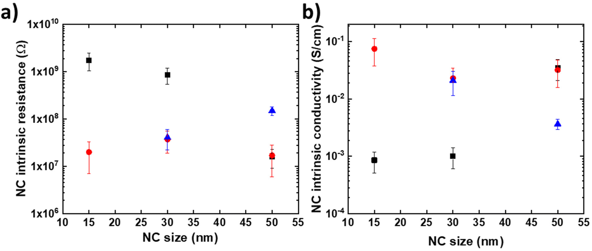 | ||
| Fig. 7 Evolution of the resistance (a) and conductivity (b) of the CsCoFe NCs extracted from the fits on the I(V) dataset: dataset #1 shown in Fig. 3 (black square symbols), dataset #2 in Fig. S3† (red circle symbols) and dataset #3 in Fig. S3† (blue triangle symbols). | ||
The main feature is that the intrinsic electron conductivity is dispersed with values between ∼5 × 10⁻² and 5 × 10⁻⁴ S cm−1 for the 15 nm NCs. A less dispersed conductivity between 2 × 10⁻² and 4 × 10⁻³ S cm−1 is estimated for the 50 nm NCs. However, there is no clear correlation between the NC intrinsic resistance, or the conductivity, with the NC size (i.e. no clear increase or decrease with size). This dispersion observed for the conductivity values on some nanocrystals mainly reflects the intrinsic dispersion of the NC structure probably inherent to the local inhomogeneities of the structure and/or chemical composition of these nano-objects. We also note that the use of an idealized truncated geometry with the nominal NC size, instead of the real shape and size, is likely to induce some dispersion of the calculated conductivity. This dispersion of the structure is inherent to the synthesis route used to fabricate these nano-objects. A full statistical, much more time-consuming, study on a larger number of nanocrystals would be considered in the future in order to better understand this conductivity dispersion.
Nevertheless, compared to sparse data in the literature, the conductivity values reported above on individual nanocrystals up to fifty times higher than those measured on PBA films: 1.5 × 10⁻⁸ to 8 × 10⁻⁷ S cm−1 for NaCo[Fe(CN6)] films42 and 5 × 10⁻⁶ to 6 × 10⁻³ S cm−1 for various Fe[Fe(CN6)], Fe [Ru(CN6)], KRu[Fe(CN6)] films.43 This work shows the importance of considering the nanocrystal individually to obtain a better estimation of its electronic properties and in particular a better estimation of its intrinsic electronic conductivity.
Conclusion
We have conducted a detailed analysis of the electronic transport properties of CsCoFe nanocrystals with a nominal size between 15 and 50 nm. We have estimated the Schottky barrier heights at the interface with HOPG and the PtIr tip of a conductive AFM. We showed that they are independent of the nanocrystal size with a value of 0.41 ± 0.02 eV at the HOPG contact and 0.27 ± 0.03 eV at the PtIr C–AFM tip contact. These values of the hole injection barrier heights (PBA valence band offset with respect to the electrode Fermi energy) are consistent with a quantum transport model that estimates hole barrier heights of ∼0.3–0.5 eV. The intrinsic electron conductivity of these CsCoFe nanocrystals was also estimated, with dispersed values between ∼5 × 10⁻⁴ S cm−1 and 2 × 10⁻² S cm−1 without any correlation with the NC shape. The origins of the conductivity inhomogeneity remain to be established, but they might be related to the dispersion of the structure and/or chemical composition of the characterized nanocrystals.Author contributions
H.T. prepared the samples (NC deposition on HOPG) and carried out all the C-AFM and TM-AFM measurements as part of his PhD thesis (supervised by S.L. and T.M.). L.C., S.M. and T.M. synthesized the PBA NCs. H.T., S.L. and D.V. analyzed the data and did the modelling. S.L. wrote the manuscript with the contributions from all authors. All authors have given approval for the final version of the manuscript.Conflicts of interest
There are no conflicts to declare.Acknowledgements
The IEMN SPM characterization facilities are partly supported by the French Network Renatech. This work has been financially supported by the French National Research Agency (ANR), project SPINFUN ANR-17-CE24-0004. We acknowledge D. Deresmes for his valuable help with the C-AFM instrument and Anne Duchêne and Clément Jamme for the TOC graphic.References
- L. Catala and T. Mallah, Nanoparticles of Prussian blue analogs and related coordination polymers: From information storage to biomedical applications, Coord. Chem. Rev., 2017, 346, 32–61, DOI:10.1016/j.ccr.2017.04.005.
- Y. L. Huang and S. Q. Ren, Multifunctional Prussian blue analogue magnets: Emerging opportunities, Appl. Mater. Today, 2021, 22100886, DOI:10.1016/j.apmt.2020.100886.
- L. Reguera, C. P. Krap, J. Balmaseda and E. Reguera, Hydrogen storage in copper Prussian blue analogues: Evidence of H-2 coordination to the copper atom, J. Phys. Chem. C, 2008, 112(40), 15893–15899, DOI:10.1021/jp803714j.
- S. S. Kaye and J. R. Long, Hydrogen storage in the dehydrated Prussian blue analogues M-3 Co(CN)(6) (2) (M = Mn, Fe, Co, Ni, Cu, Zn), J. Am. Chem. Soc., 2005, 127(18), 6506–6507, DOI:10.1021/ja051168t.
- K. W. Chapman, P. D. Southon, C. L. Weeks and C. J. Kepert, Reversible hydrogen gas uptake in nanoporous Prussian Blue analogues, Chem. Commun., 2005,(26), 3322–3324, 10.1039/b502850g.
- W. J. Li, C. Han, G. Cheng, S. L. Chou, H. K. Liu and S. X. Dou, Chemical Properties, Structural Properties, and Energy Storage Applications of Prussian Blue Analogues, Small, 2019, 15(32), 1900470, DOI:10.1002/smll.201900470.
- H. C. Yi, R. Z. Qin and S. X. Ding, et al., Structure and Properties of Prussian Blue Analogues in Energy Storage and Conversion Applications, Adv. Funct. Mater., 2021, 31(6), 2006970, DOI:10.1002/adfm.202006970.
- J. F. Qian, C. Wu and Y. L. Cao, et al., Prussian Blue Cathode Materials for Sodium-Ion Batteries and Other Ion Batteries, Adv. Energy Mater., 2018, 8(17), 1702619, DOI:10.1002/aenm.201702619.
- Y. X. Xu, S. S. Zheng, H. F. Tang, X. T. Guo, H. G. Xue and H. Pang, Prussian blue and its derivatives as electrode materials for electrochemical energy storage, Energy Storage Mater., 2017, 9, 11–30, DOI:10.1016/j.ensm.2017.06.002.
- C. Tannous and R. L. Comstock, Magnetic Information-Storage Materials, in Springer Handbook of Electronic and Photonic Materials, ed. S. Kasap and P. Capper, Springer International Publishing, 2017, pp. 1 Search PubMed.
- Y. Matos-Peralta and M. Antuch, Review-Prussian Blue and Its Analogs as Appealing Materials for Electrochemical Sensing and Biosensing, J. Electrochem. Soc., 2019, 167(1), 037510, DOI:10.1149/2.0102003jes.
- B. Nayebi, K. P. Niavol and S. Y. Kim, et al., Prussian blue-based nanostructured materials: Catalytic applications for environmental remediation and energy conversion, Mol. Catal., 2021, 514111835, DOI:10.1016/j.mcat.2021.111835.
- Y. Kamachi, M. B. Zakaria and N. L. Torad, et al., Hydrogels Containing Prussian Blue Nanoparticles Toward Removal of Radioactive Cesium Ions, J. Nanosci. Nanotechnol., 2016, 16(4), 4200–4204, DOI:10.1166/jnn.2016.12607.
- K. M. Lee, T. Kawamoto and K. Minami, et al., Improved adsorption properties of granulated copper hexacyanoferrate with multi-scale porous networks, RSC Adv., 2016, 6(20), 16234–16238, 10.1039/c5ra25388h.
- M. A. Busquets and J. Estelrich, Prussian blue nanoparticles: synthesis, surface modification, and biomedical applications, Drug Discovery Today, 2020, 25(8), 1431–1443, DOI:10.1016/j.drudis.2020.05.014.
- H. J. Buser, D. Schwarzenbach, W. Petter and A. Ludi, Crystal-Structure of Prussian Blue – Fe4[Fe(Cn)6]3.Xh2o, Inorg. Chem., 1977, 16(11), 2704–2710 CrossRef CAS.
- D. F. Shriver and D. B. Brown, Environment of interstitial ions in a Prussian blue analog, Co3[Co(CN)6]2, Inorg. Chem., 1969, 8(1), 42–46, DOI:10.1021/ic50071a010.
- D. B. Brown and D. F. Shriver, Structures and solid-state reactions of Prussian blue analogs containing chromium, manganese, iron, and cobalt, Inorg. Chem., 1969, 8(1), 37–42, DOI:10.1021/ic50071a009.
- D. Brinzei, L. Catala and N. Louvain, et al., Spontaneous stabilization and isolation of dispersible bimetallic coordination nanoparticles of CsxNi Cr(CN)(6)(y), J. Mater. Chem., 2006, 16(26), 2593–2599, 10.1039/b605221e.
- L. Catala, D. Brinzei and Y. Prado, et al., Core-Multishell Magnetic Coordination Nanoparticles: Toward Multifunctionality on the Nanoscale, Angew. Chem., Int. Ed., 2009, 48(1), 183–187 CrossRef.
- S. Cobo, G. Molnar and F. Carcenac, et al., Thin Films of Prussian Blue: Sequential Assembly, Patterning and Electron Transport Properties at the Nanometric Scale, J. Nanosci. Nanotechnol., 2010, 10(8), 5042–5050, DOI:10.1166/jnn.2010.2430.
- D. M. Pajerowski, T. Watanabe, T. Yamamoto and Y. Einaga, Electronic conductivity in Berlin green and Prussian blue, Phys. Rev. B: Condens. Matter Mater. Phys., 2011, 83(15), 153202, DOI:10.1103/PhysRevB.83.153202.
- C. Lefter, R. Tan and J. Dugay, et al., Light induced modulation of charge transport phenomena across the bistability region in Fe(Htrz)(2)(trz) (BF4) spin crossover micro-rods, Phys. Chem. Chem. Phys., 2015, 17(7), 5151–5154, 10.1039/c4cp05250a.
- R. Bonnet, S. Lenfant, S. Mazerat, T. Mallah and D. Vuillaume, Long-range electron transport in Prussian blue analog nanocrystals, Nanoscale, 2020, 12(39), 20374–20385, 10.1039/d0nr06971j.
- S. Datta, Electronic transport in mesoscopic systems, Cambridge University Press, 1997 Search PubMed.
- J. C. Cuevas and E. Scheer, Molecular electronics: an introduction to theory and experiment, World Scientific, 2010 Search PubMed.
- I. Tanaka, I. Kamiya and H. Sakaki, Local surface band modulation with MBE-grown InAs quantum dots measured by atomic force microscopy with conductive tip, J. Cryst. Growth, 1999, 201, 1194–1197 CrossRef.
- J. Oh and R. J. Nemanich, Current–voltage and imaging of TiSi2 islands on Si (001) surfaces using conductive-tip atomic force microscopy, J. Appl. Phys., 2002, 92(6), 3326–3331 CrossRef CAS.
- M. Rezeq, Y. Abbas, B. Wen, Z. Wasilewski and D. Ban, Direct detection of electronic states for individual indium arsenide (InAs) quantum dots grown by molecular beam epitaxy, Appl. Surf. Sci., 2022, 590, 153046 CrossRef CAS.
- A. Grillo and A. Di Bartolomeo, A Current-Voltage Model for Double Schottky Barrier Devices, Adv. Electron. Mater., 2021, 7(2), 2000979, DOI:10.1002/aelm.202000979.
- E. H. Rhoderick and R. H. Williams, Metal-semiconductor contacts, Clarendon Press, Oxford, 1988, vol. 129 Search PubMed.
- R. T. Tung, Electron transport of inhomogeneous Schottky barriers, Appl. Phys. Lett., 1991, 58(24), 2821–2823, DOI:10.1063/1.104747.
- R. T. Tung, Electron transport at metal-semiconductor interfaces: General theory, Phys. Rev. B: Condens. Matter Mater. Phys., 1992, 45(23), 13509–13523, DOI:10.1103/PhysRevB.45.13509.
- F. Ruffino, M. G. Grimaldi, F. Giannazzo, F. Roccaforte and V. Raineri, Size-dependent Schottky barrier height in self-assembled gold nanoparticles, Appl. Phys. Lett., 2006, 89, 243113 CrossRef.
- H. Hasegawa, T. Sato and S. Kasai, Unpinning of Fermi level in nanometer-sized Schottky contacts on GaAs and InP, Appl. Surf. Sci., 2000, 166(1–4), 92–96 CrossRef CAS.
- L. Trinh, S. Zerdane and S. Mazerat, et al., Photoswitchable 11 nm CsCoFe Prussian Blue Analogue Nanocrystals with High Relaxation Temperature, Inorg. Chem., 2020, 59(18), 13153–13161, DOI:10.1021/acs.inorgchem.0c01432.
- Y. Prado, S. Mazerat and E. Riviere, et al., Magnetization Reversal in (CsNiCrIII)-Cr-II(CN)(6) Coordination Nanoparticles: Unravelling Surface Anisotropy and Dipolar Interaction Effects, Adv. Funct. Mater., 2014, 24(34), 5402–5411 CrossRef CAS.
- J. C. Wojdeł, I. d. P. R. Moreira, S. T. Bromley and F. Illas, On the prediction of the crystal and electronic structure of mixed-valence materials by periodic density functional calculations: The case of Prussian Blue, J. Chem. Phys., 2008, 128(4), 044713, DOI:10.1063/1.2824966.
- S. Watanabe, Y. Sawada and M. Nakaya, et al., Intra- and inter-atomic optical transitions of Fe, Co, and Ni ferrocyanides studied using first-principles many-electron calculations, J. Appl. Phys., 2016, 119(23), 235102, DOI:10.1063/1.4954070.
- D. R. Rosseinsky, J. S. Tonge, J. Berthelot and J. F. Cassidy, Site-transfer conductivity in solid iron hexacyanoferrates by dielectric relaxometry, voltammetry and spectroscopy - prussian blue, congeners and mixtures, J. Chem. Soc., Faraday Trans. 1, 1987, 83, 231–243, 10.1039/f19878300231.
- A. Xidis and V. D. Neff, On the electronic conduction in dry thin-films of prussian blue, prussian yellow, and everitt salt, J. Electrochem. Soc., 1991, 138(12), 3637–3642, DOI:10.1149/1.2085472.
- O. Sato, T. Kawakami, M. Kimura, S. Hishiya, S. Kubo and Y. Einaga, Electric-field-induced conductance switching in FeCo Prussian blue analogues, J. Am. Chem. Soc., 2004, 126(41), 13176–13177, DOI:10.1021/ja046329s.
- J. N. Behera, D. M. D'Alessandro, N. Soheilnia and J. R. Long, Synthesis and Characterization of Ruthenium and Iron-Ruthenium Prussian Blue Analogues, Chem. Mater., 2009, 21(9), 1922–1926, DOI:10.1021/cm900230p.
- L. Amirav and M. Wachtler, Nano Schottky?, Nano Lett., 2022, 22(24), 9783–9785, DOI:10.1021/acs.nanolett.2c04150.
- S. Angizi, P. R. Selvaganapathy and P. Kruse, Graphene-silicon Schottky devices for operation in aqueous environments: Device performance and sensing application, Carbon, 2022, 194, 140–153, DOI:10.1016/j.carbon.2022.03.052.
- H.-Y. Liu, J. Yin and X. Gao, et al., Scalable Submicron Channel Fabrication by Suspended Nanofiber Lithography for Short-Channel Field-Effect Transistors, Adv. Funct. Mater., 2022, 32(6), 2109254, DOI:10.1002/adfm.202109254.
- S. M. Sze, Physics of Semiconductor Devices, 1981, pp. 1–442 Search PubMed.
- D. J. Wold and C. D. Frisbie, Fabrication and characterization of metal-molecule-metal junctions by conducting probe atomic force microscopy, J. Am. Chem. Soc., 2001, 123, 5549–5556 CrossRef CAS.
- G. Felix, M. Mikolasek and H. J. Shepherd, et al., Elasticity of Prussian-Blue-Analogue Nanoparticles, Eur. J. Inorg. Chem., 2018,(3–4), 443–448, DOI:10.1002/ejic.201700796.
- A. Bleuzen, J. D. Cafun and A. Bachschmidt, et al., CoFe Prussian Blue Analogues under Variable Pressure. Evidence of Departure from Cubic Symmetry: X-ray Diffraction and Absorption Study, J. Phys. Chem. C, 2008, 112(45), 17709–17715, DOI:10.1021/jp805852n.
- D. P. Long, J. L. Lazorcik and B. A. Mantooth, et al., Effects of hydration on molecular junction transport, Nat. Mater., 2006, 5, 901–908 CrossRef CAS PubMed.
- X. Zhang, S. A. Mcgill and P. Xiong, Origin of the humidity sensitivity of Al/AlO(x)/MHA/Au molecular tunnel junctions, J. Am. Chem. Soc., 2007, 129(46), 14470–14474, DOI:10.1021/ja0758988.
- K. Smaali, N. Clément, G. Patriarche and D. Vuillaume, Conductance Statistics from a Large Array of Sub-10 nm Molecular Junctions, ACS Nano, 2012, 6(6), 4639–4647, DOI:10.1021/nn301850g.
- W. N. Hansen and G. J. Hansen, Standard reference surfaces for work function measurements in air, Surf. Sci., 2001, 481(1–3), 172–184, DOI:10.1016/s0039-6028(01)01036-6.
- N. J. Lee, J. W. Yoo and Y. J. Choi, et al., The interlayer screening effect of graphene sheets investigated by Kelvin probe force microscopy, Appl. Phys. Lett., 2009, 95(22), 222107, DOI:10.1063/1.3269597.
- S. Banerjee, M. Sardar, N. Gayathri, A. K. Tyagi and B. Raj, Conductivity landscape of highly oriented pyrolytic graphite surfaces containing ribbons and edges, Phys. Rev. B: Condens. Matter Mater. Phys., 2005, 72(7), 075418, DOI:10.1103/PhysRevB.72.075418.
- J. Oswald, D. Beretta and M. Stiefel, et al., Field and Thermal Emission Limited Charge Injection in Au–C60–Graphene van der Waals Vertical Heterostructures for Organic Electronics, ACS Appl. Nano Mater., 2023, 6, 9444–9452, DOI:10.1021/acsanm.3c01090.
- C. H. Kim, O. Yaghmazadeh, D. Tondelier, Y. B. Jeong, Y. Bonnassieux and G. Horowitz, Capacitive behavior of pentacene-based diodes: Quasistatic dielectric constant and dielectric strength, J. Appl. Phys., 2011, 109(8), 083710, DOI:10.1063/1.3574661.
Footnote |
| † Electronic supplementary information (ESI) available. See DOI: https://doi.org/10.1039/d3nr04542k |
| This journal is © The Royal Society of Chemistry 2023 |