
 Open Access Article
 This Open Access Article is licensed under a
 Creative Commons Attribution 3.0 Unported Licence
Compositional defects in a MoAlB MAB phase thin film grown by high-power pulsed magnetron sputtering†
Rajib
Sahu‡
 *ab,
Dimitri
Bogdanovski‡
*b,
Jan-Ole
Achenbach
b,
Marcus
Hans
b,
Daniel
Primetzhofer
c,
Jochen M.
Schneider
ab and
Christina
Scheu
*ad
*ab,
Dimitri
Bogdanovski‡
*b,
Jan-Ole
Achenbach
b,
Marcus
Hans
b,
Daniel
Primetzhofer
c,
Jochen M.
Schneider
ab and
Christina
Scheu
*ad
aMax-Planck-Institut für Eisenforschung GmbH, Max-Planck-Str. 1, 40237 Düsseldorf, Germany. E-mail: r.sahu@mpie.de; scheu@mpie.de
bMaterials Chemistry, RWTH Aachen University, Kopernikusstr. 10, 52074 Aachen, Germany. E-mail: bogdanovski@mch.rwth-aachen.de
cDepartment of Physics and Astronomy, Uppsala University, Box 516, S-75120 Uppsala, Sweden
dMaterials Analytics, RWTH Aachen University, Kopernikusstr. 10, 52074 Aachen, Germany
First published on 25th October 2023
Abstract
Various compositional defects such as Mo3Al2B4, Mo4Al3B4, Mo6Al5B6 and Al3Mo, together with MoB MBene, are observed to be coexisting in a MoAlB MAB phase thin film grown at 800 °C by high-power pulsed magnetron sputtering. An overall film composition of Mo0.29Al0.33B0.38 is measured by time-of-flight elastic recoil detection analysis. The concurrent formation of these compositional defects in the MoAlB matrix occurs during the synthesis without using any chemical reagent, and their coexistence with the MAB phase is thermodynamically possible, as elucidated by density functional theory simulations. These defect phases are imaged at the atomic scale by aberration-corrected scanning transmission electron microscopy. A rough estimation of defect populations of 0.073, 0.037, 0.042 and 0.039 nm−1 for Mo3Al2B4, Mo4Al3B4, Mo6Al5B6 and Al3Mo compositional defects, respectively, is performed within the MoAlB matrix. The calculated energies of formation reveal that the Mo4Al3B4 and Mo6Al5B6 defect phases form spontaneously in the MoAlB host matrix, while the energy barrier towards the formation of the metastable Mo3Al2B4 phase is approx. 20 meV per atom. The small magnitude of this barrier is easily overcome during vapor phase condensation, and the surface diffusion of adatoms during deposition leads to local compositional variations and the coexistence of the defect phases in the host matrix. Additionally, at grain boundaries, the presence of MoB MBene is observed, with an interlayer spacing between two Mo2B2 units increasing up to ∼50% compared to the pristine MoAlB phase.
1. Introduction
Layered ternary transition metal boride (MAB) phases, e.g. molybdenum aluminum boride, are known as ceramic nanolaminates,1,2 possessing a unique combination of ceramic and metallic properties: the M–A bond shows metallic character, while the M–B bond presents a mixed covalent/metallic/ionic interaction in MAB phases.3 MoAlB is one of the most studied and representative materials among these nanolaminates, with applications as protective coatings4,5 and electrode materials6,7 due to its excellent electrical and thermal conductivities,2 high hardness, fracture toughness,8 corrosion resistance,8 and high temperature stability.8,9 Moreover, MoAlB is also used as a precursor material to synthesize its two-dimensional (2D) MoB MBene derivative10,11 to improve energy conversion and storage applications. It is reasonable to assume that all these properties are significantly influenced by the presence of structural and compositional defects. The formation of compositional defects such as Mo4Al3B4 and Mo6Al5B6 upon chemical etching in a bulk MoAlB phase synthesized at 1400 °C was observed in the literature.10The synthesis of the orthorhombic MoAlB MAB phase at a lower temperature of 700 °C compared to prior literature procedures (above 1000 °C for the bulk phase)6,7,10 was established by our group and reported earlier.5,11–13 Various multi-dimensional defect phases (1D to 3D) have been found11,13 in a film grown by direct current (DC) magnetron sputtering at 700 °C. In this work, we demonstrate that other previously unobserved compositional defects occur upon synthesis of a MoAlB thin film via high-power pulsed magnetron sputtering (HPPMS) at 800 °C. The said defects exhibit the compositions Mo3Al2B4, Mo4Al3B4, Mo6Al5B6 and Al3Mo and are observed within a MoAlB grain and characterized at the atomic scale with aberration-corrected scanning transmission electron microscopy (STEM). Furthermore, all defects are shown to be very close in terms of their energy of formation to the MoAlB main phase via density functional theory (DFT) calculations, providing a thermodynamic explanation for their concurrent formation and coexistence. A rough estimation of the defect population within a MoAlB grain is performed. Furthermore, the formation of MBene MoB is also observed at the grain boundaries with a low fraction and consisting of delaminated Mo2B2 units with an interlayer spacing increased by ∼50% when compared to MoAlB. Thus, we provide the first structural description of Mo4Al3B4, Mo6Al5B6 and Al3Mo defect phases formed in a MoAlB thin film matrix during physical vapor deposition, i.e. without using any chemical etching agents, which was hitherto unreported.
2. Experimental section
2.1. Thin film growth
The MoAlB thin films were grown on single-crystal Al2O3 (0001)-oriented substrates via physical vapor deposition using HPPMS at 800 °C (substrate temperature). A two-inch compound MoAlB target (Plansee Composite Materials GmbH) with a composition of 33.33 at% Mo, Al and B each was used, with an average target power of 100 W during the sputtering process, a pulse-on time of 100 μs and an overall pulse length of 500 μs (thus, a duty cycle of 20%). The substrate-to-target distance was kept at around 10 cm. The deposition pressure was 0.35 Pa using Ar as the working gas. After a deposition time of 3 h, the final thickness of the coating was approx. 2.6 μm as measured on cross-sectional TEM micrographs.2.2. Elastic recoil detection analysis
Depth profiling of the composition was done by time-of-flight elastic recoil detection analysis (ToF-ERDA) at the Tandem Laboratory of Uppsala University.14 The primary ion beam of 127I8+ at 36 MeV energy reached the film surface at an angle of 67.5° with respect to the normal, and recoils were detected at an angle of 45° with respect to the primary beam (both incidence and exit angles of 22.5°). The detection telescope consisted of thin carbon foils for the ToF measurement as well as a solid-state detector.15 Bulk borides were used as reference samples and the total measurement uncertainty was <5% relative to the deduced values.2.3. Transmission electron microscopy
A probe-corrected ThermoFisher Titan Themis was used for STEM experiments at an operating voltage of 300 kV. Both cross-sectional and plan-view TEM samples were prepared by conventional mechanical polishing and Ar ion milling in a Gatan PIPS system. Samples were thinned down below ∼35 nm for high-resolution (HR) STEM imaging. A convergence angle of 23.8 mrad was chosen and ranges of 0–8, 10–16, 18–34 and 78–200 mrad were set as the collection angles for bright field (BF), annular bright field (ABF), annular dark field (ADF) and high-angle annular dark field (HAADF) imaging, respectively. The microscope was equipped with a Bruker SuperX detector for energy-dispersive X-ray spectroscopy (EDX) analysis. The analysis of the defect population using STEM micrographs is discussed in the following.3. Density functional theory
The individual defect phases Mo3Al2B4, Mo4Al3B4 and Mo6Al5B6 were modeled as bulk-like periodic systems to estimate their energies of formation in the ground state via DFT calculations in comparison with the pristine MoAlB phase. The structural model for the latter was taken from the literature16 and used as a starting point to manually generate the individual defect-containing phases, mimicking the morphology observed in the STEM micrographs of our study and in previous literature13 by insertion of additional atoms and shifting of adjacent atoms along the b direction. The structural models generated are thus shown in the Results and discussion section and will be discussed further there.Full structural optimization of the obtained models was performed using the Vienna ab initio simulation package (VASP, version 5.4.4., University of Vienna),17–19 utilizing projector-augmented waves (PAW)20 for basis set generation with a cutoff energy of 500 eV. To account for electronic exchange and correlation effects, the well-established parametrization of the generalized gradient approximation by Perdew, Burke and Ernzerhof (PBE)21 was employed, with “semi-core” electron configurations used in the atomic potentials generating the basis sets: 5s24d44s24p6 for Mo, 3s23p1 for Al and 2s22p1 for B. The Methfessel–Paxton22 scheme was employed for Brillouin zone integration along a k-mesh of 14 × 1 × 14 points (corresponding to the a, b, and c crystallographic directions) generated by the Monkhorst–Pack method.23 This mesh size has been shown to be sufficient to ensure energetic and force convergence in prior tests.
The total ground-state energies of the fully optimized structures were then used to calculate the energies of formation at 0 K vs. the constituting elements (bcc Mo, fcc Al and α-B) by subtracting the summed energies of the starting materials from the total energy of the defect phase in question, accounting for correct stoichiometric coefficients.
4. Results and discussion
The overall microstructure of the as-deposited MoAlB MAB phase thin film grown by HPPMS is imaged in both plan view and cross-section directions. The diameter of the grains measured in the top view is approx. 100–150 nm. There are pores with a size of 30–60 nm in the examined sample (white arrows in Fig. 1a). This is a much smaller value compared to the one observed in our previous film deposited by DC sputtering,11,13 which is around 120–170 nm (see ESI, Fig. S1†). A cross-sectional image in Fig. 1b shows characteristic columnar growth and the majority of the grains are slightly inclined (white dotted arrows) to the substrate Al2O3. Following nucleation on the substrate surface, the seed crystals grow and coalescence results in 20–50 nm wide columnar-like grains. Over time, as deposition continues, the columns coarsen and competitive growth results in columns that extend from the substrate to the near-surface region. A detailed discussion on columnar grain growth is available.24 The average grain length ranges between 800 and 1400 nm, which is 2–3 times lower than the total film thickness.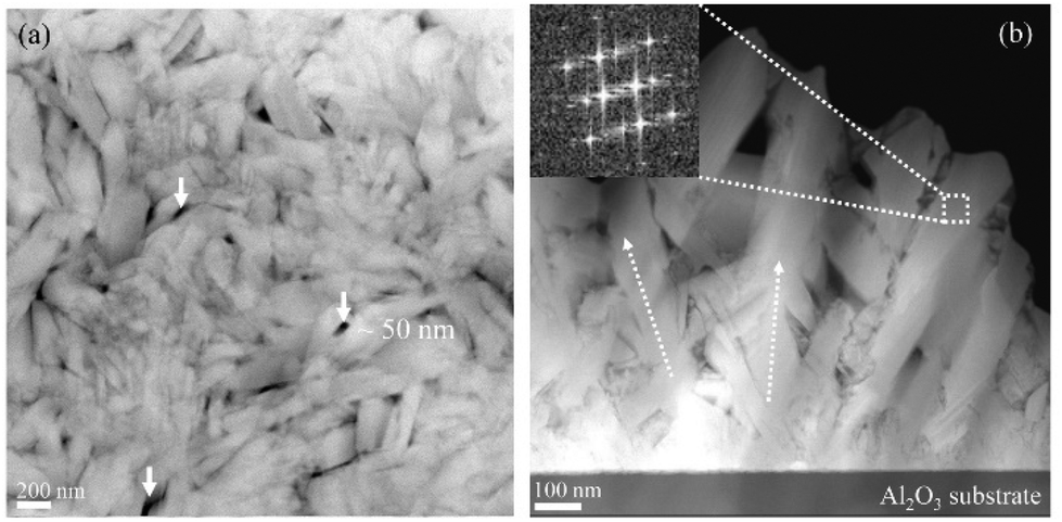 | ||
| Fig. 1 Overview of a MoAlB thin film in (a) plan view and (b) cross-sectional STEM images. White solid arrows mark pores in the films. Dotted arrows show the long axis of the grains. The fast Fourier transformation (calculated from the white dotted rectangle) confirms the presence of an orthorhombic MoAlB phase and is shown as the inset. | ||
Before discussing the defects in detail, it is worth mentioning that the fast Fourier transformation (FFT) (inset in Fig. 1b) confirms that the MoAlB matrix possesses an orthorhombic crystal structure, with lattice parameters in accordance with literature values (a = 3.18 Å, b = 14.12 Å and c = 3.12 Å).5 Selected area diffraction patterns are available in the ESI (Fig. S2†). Similar to a film synthesized via DC sputtering,11,13 both Al-rich and O-rich impurity phases are also observed here. Elemental composition mapping of Mo, Al and O by STEM EDX is available in the ESI (Fig. S3†). Depth profiling by ToF-ERDA reveals a homogeneous composition of Mo0.29Al0.33B0.38 with Mo/Al and Mo/B ratios of 0.91 and 0.79, respectively, indicating an overall off-stoichiometric composition similar to the DC sputtered film with a composition of Mo0.31Al0.32B0.37.11 However, densification of the film through employment of HPPMS causes a significantly lower oxygen content of ∼2 at% vs. ∼4 at% obtained after DC sputtering; this densification reduces oxygen incorporation through atmospheric exposure, which is also governed by the film morphology.25 The ERDA depth profile is provided in the ESI (Fig. S4†). Further structural defect analysis at the atomic scale is described in later sections.
Growth-kinetics-induced defects, including compositional defects (CDs), in the MoAlB system were already reported in films synthesized by DC magnetron sputtering.11,13 Al deintercalation by chemical etching is commonly employed, leading to CD formation in the MoAlB bulk phase.7,10,26 The synthesis of various metastable CDs in the present approach of thin film growth without using any external chemical reagent and their characterization are discussed here. The 434-type (referring here, and further throughout, to the stoichiometric coefficients of Mo, Al and B in the compound in question) Mo4Al3B4 MAB phase (red arrows) and the 324-type Mo3Al2B4 (white arrows) phase are shown in the ADF STEM micrograph in Fig. 2a. Low magnification imaging over the grain boundary region reveals the extension of the Mo4Al3B4 phase (dotted red bracket) across two grains. As the intensity in HAADF STEM is roughly proportional to Z2 (where Z is the atomic number),27 the bright atomic columns are Mo atoms and dark grey ones are Al, while B is not detectable due to the low atomic number. As described below, the position of B atomic columns will be depicted in ABF STEM images. A magnified HAADF STEM micrograph illustrates coexisting 222-type MoAlB and 434-type Mo4Al3B4 MAB phases within the grain interior (Fig. 2b). A single unit of a Mo4Al3B4 MAB phase (in the cb plane) is marked by a double-headed red arrow in Fig. 2b, with an overlaid structural model of Mo (purple dots), Al (blue dots) and B (green dots) marking the individual atomic positions (inset Fig. 2b). The presence of an interlayer spacing of 2.6 ± 0.1 Å between neighboring Mo2B2 subunits indicates the pristine MoAlB phase, while a spacing distance of 1.7 ± 0.1 Å is calculated for the Mo4Al3B4 area. More images of Mo4Al3B4 defects from other grains are provided in the ESI (Fig. S5†). A detailed discussion of the Mo3Al2B4 compositional defect is provided in a later section.
 | ||
| Fig. 2 (a) Low-magnification ADF STEM image showing various CDs. White and red arrows mark the Mo3Al2B4 and Mo4Al3B4 phases, respectively. (b) Coexisting MoAlB–Mo4Al3B4 phases at higher magnification (the white square box in (a)) shown in HAADF STEM. Interlayer spacing measurements are marked by red and black lines. (c) HAADF image depicting the Mo6Al5B6 MAB phase (blue arrows). (d) Single units of Mo6Al5B6 are marked by double-headed blue arrows in a HRSTEM image (acquired from a different grain). Mo2B2 units (black arrows) rotated by 90° are identified inside the Mo6Al5B6 phase. White arrows mark a single Al layer between [100] and tilted [001] Mo2B2 units. (e) and (f) Enlarged HAADF and ABF STEM micrographs of the Mo6Al5B6 defect. The structural model overlays depicted in (b), (e) and (f) mark Mo (purple), Al (blue) and B (green) atoms. | ||
The HAADF STEM micrograph in Fig. 2c reveals an additional 656-type Mo6Al5B6 defect phase (blue arrows) inside the MoAlB matrix, with each double-headed blue arrow in the high-resolution STEM image in Fig. 2d indicating a single unit of this phase at the atomic scale. Interestingly, some of the Mo6Al5B4 layers are defective, with one Mo2B2 unit rotated by 90°, similar to the observations in twist grain boundaries.11,13 The rotated Mo2B2 units are identified and marked by black arrows inside the Mo6Al5B6 layers. A single Al layer (white arrows) is sandwiched between Mo2B2 units aligned along the [100] zone axis and its [001] tilt boundary. More details of twist grain boundaries in this film are available in the ESI (Fig. S5 and S6†). Combined HAADF (Fig. 2e) and ABF STEM (Fig. 2f) micrographs at a higher magnification visualize the structure of a Mo6Al5B6 unit, with an overlay similar to that in Fig. 2d.
Furthermore, the coexistence of molybdenum aluminate (Al3Mo) and MoAlB phases inside the MoAlB matrix is observed and shown in HAADF STEM in Fig. 3a. In-depth analyses predict the formation of an Al3Mo phase, which is well known in the Mo–Al compound system28–30 in this temperature range. White arrows mark the Al3Mo phase at the atomic scale. Both Mo and Al atoms are identified and marked by purple and blue dots to reveal the atomic arrangement in this structural fault. A magnified section (marked by the white dotted rectangle) of the molybdenum aluminate region in the HRSTEM micrograph (Fig. 3b) shows a Mo atomic plane (purple dots) sandwiched between an Al bilayer (bottom) and trilayer (top). Two different interlayer spacings of ∼3.54 ± 0.08 Å and 2.46 ± 0.08 Å (indicated by black and red arrows, respectively) are measured in HAADF STEM. An Al double layer exhibits an ∼2.5 ± 0.1 Å projected distance (ab plane) between individual Mo2B2 units in the MoAlB phase. Analyzing and collating the corresponding BF, ABF and ADF STEM images in Fig. 3c–e, a strong indication for the existence of the Al3Mo phase is evident. Images of similar defects from different regions are presented in the ESI (Fig. S7†). Moreover, combined high-resolution HAADF STEM micrographs and geometrical phase analysis (GPA)31 provide quantitative maps of the local lattice distortion at the phase boundary of Al3Mo–MoAlB in Fig. 3f. This map is derived from the variation in interplanar spacing calculated by comparing it to the reference undistorted MoAlB region, highlighted in a red rectangle (Fig. 3f). The color scale used in this map corresponds to the upper (1%) and lower (−1%) limits of the total relative interplanar spacing difference (εxx). Additional components of the relative interplanar spacing difference tensor (εyy) are shown in the ESI (Fig. S8†).
 | ||
| Fig. 3 Coexisting molybdenum aluminate (Al3Mo) and MoAlB phases inside the MoAlB matrix is identified by white arrows in the HAADF STEM image (a). Atomic arrangement of Mo (purple), Al (blue) and B (green) at the interface of the Al3Mo–MoAlB region is marked by combining (b) HAADF, (c) BF, (d) ABF and (e) ADF STEM micrographs. Local lattice distortion mapping (εxx) at the phase boundary of Al3Mo–MoAlB is shown in (f). The corresponding region is marked in (a) by a black rectangle. | ||
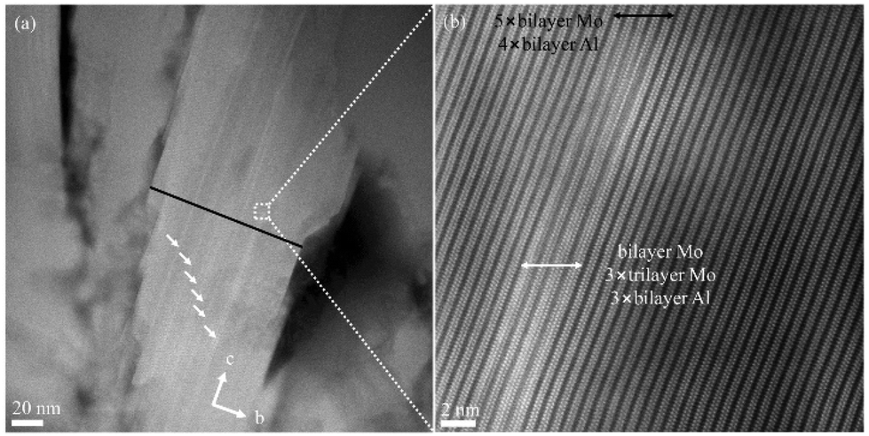
The 324-type Mo3Al2B4 MAB defect phase shown in the cross-sectional HAADF STEM micrograph (Fig. 4) was already observed in our earlier DC sputtered films.13 However, in the present film synthesized via HPPMS, a much higher density of these CDs (marked by white arrows in Fig. 4a) was observed compared to the single-layer Mo3Al2B4 formation after DC sputtering.11,13 A rough phase fraction of all the outlined defects is given in the following section. Specific atomic column counting (Mo, Al and B) and measurements of the interlayer spacing indicate a compositional change from MoAlB to Mo3Al2B4 (Fig. 4b). The double-headed black arrow signifies a phase-pure MoAlB region with 5× bilayer Mo and 4× bilayer Al columns in Fig. 4b. Examining a similar area in the vicinity of the CD (double-headed white arrow), we notice that bilayer Mo, 3× trilayer Mo and 3× bilayer Al columns exist. Hence, the presence of Mo3Al2B4 is observed, consistent with the loss of an Al bilayer. The formation of Mo3Al2B4 phases in a MoAlB matrix is thermodynamically plausible due to the very small differences in formation energy calculated by DFT simulations.13 More HAADF STEM micrographs from different grains are provided in the ESI (Fig. S9†).
 | ||
| Fig. 4 Cross-sectional HAADF STEM image of the Mo3Al2B4 compositional defect (indicated by white arrows) viewed in the [100] zone axis. (a) The region where a MoAlB–Mo3Al2B4 composition change occurs is identified. | ||
A rough estimation of the fractions of these described defect phases is performed by measuring the maximum number of intersection points of the CDs within a given length inside a MoAlB grain, thus obtaining a defect population. As an example, we illustrate the estimation of the Mo3Al2B4 defect phase population in one given grain: a line with a length of 110 nm is drawn perpendicular to the CD (indicated by the black line in Fig. 4a). Then the total number of CD sections is divided by the length of the black line, yielding a maximum population of ∼0.073 nm−1. Similar measurements were carried out for all defect phases. Average populations of 0.037, 0.042 and 0.039 nm−1 for the Mo4Al3B4, Mo6Al5B6 and Al3Mo phases within the MoAlB matrix were calculated, respectively. The corresponding line sectioning grains of these defect phases are available in the ESI (Fig. S5–S7†).
Apart from various CDs, frequently observed 2D MoB MBene regions at grain boundaries are shown in Fig. 5. HAADF STEM reveals MoB units without Al layers, marked by the dotted line and the bracket (Fig. 5a and b). Similar to our previous report,11 we observed Al deintercalation and local oxidation, leading to the formation of a 2D MoB MBene–AlOx heterostructure at the grain boundary. Chemical analysis by STEM EDX and its relative elemental intensity distribution are provided in the ESI (Fig. S10†). A significant increase in interlayer spacing between two neighboring Mo2B2 units is observed (double-headed white arrow) with an approximate value of 4.0 ± 0.2 Å (Fig. 5a), in contrast to a spacing in the range of ∼2.7 ± 0.1 Å in the pristine MoAlB MAB phase. Also, over an estimated length of ∼2 nm, MoB layer detachment (indicated by white dotted arrows) is marked as a 2D MBene feature in Fig. 5b. More images of MBene regions from various grains are provided in the ESI (Fig. S11†).
 | ||
| Fig. 5 2D MoB MBene layers (white dotted lines and a bracket) from two different grains of the film are shown in (a) and (b). A delaminated two-dimensional MoB layer is indicated by white dotted arrows in (b). | ||
To gauge the energetics of the experimentally observed concurrent presence of multiple defect types in the MoAlB matrix, we have studied the energies of formation in the ground state via DFT calculations for Mo3Al2B4, Mo4Al3B4 and Mo6Al5B6 (the B-free Al3Mo phase was not considered). In these phases, the structural models replicated the morphology of the defects observed via STEM as closely as possible and preserved the stoichiometric ratios of 324, 434 and 656, respectively; however, due to computational constraints demanding periodicity, they were modeled as bulk phases and not as isolated regions in the host matrix. 2 × 1 × 1 supercells of the corresponding structural models are shown as projections in the ab plane (viewed along the c direction) in Fig. 6a, while their corresponding energies of formation are depicted in Fig. 6b.
 | ||
| Fig. 6 (a) Structural models used in the DFT calculations of Mo3Al2B4, Mo4Al3B4 and Mo6Al5B6, from top to bottom, projected in the ab plane. For a clearer visualization of the morphology, 2 × 1 × 1 supercells are shown. Mo atoms are purple, Al atoms are blue, and B atoms are green. (b) Energies of formation at 0 K, relative to that of MoAlB, for all depicted defects and a Mo3Al2B4-like structural model containing one B vacancy (not shown in (a)). The green area signifies an energetic region where the formation of defects from the elements is more advantageous than that of MoAlB. | ||
In relation to the morphology, the defect phases Mo4Al3B4 and Mo6Al5B6 are closely related: along b, the former phase exhibits blocks of two Mo and two B layers each, followed by a single Al layer and another block of two Mo and B layers. Then, an Al bilayer separates the described structural subunit from an identical one which is shifted by 0.5 a, as seen in the middle structural model in Fig. 6a. The Al layer stacking can thus be described as dual–single–dual–single etc. In contrast, in the Mo6Al5B6 phase (bottom structural model in Fig. 6a), the double Al layers are bracketing a single block of two Mo and two B layers, followed by two such blocks, both shifted by 0.5 a, and separated from each other by a single Al layer, with the corresponding Al layer stacking now being dual–dual–single–dual–dual etc. Hence, a broad structural similarity of both defect phases is evident, especially in contrast to the Mo3Al2B4 model, in which blocks of three Mo layers and four B layers in total are separated by Al dual layers and again shifted by 0.5 a in relation to each other.
These general trends are reflected in the energies of formation at 0 K, ΔEf, referenced to that of pristine MoAlB as the baseline, as shown in Fig. 6b. We immediately noted that the energies of formation for Mo4Al3B4 and Mo6Al5B6 are nearly identical, congruent with the structural similarity; furthermore, interestingly, both lie in the negative energy region, indicating favored formation vs. pristine MoAlB. However, the energetic difference is minuscule, lying between 2 and 5 meV per atom, and likely has no physical meaning, stemming from the numerical error inherent in the DFT simulation. In contrast, the energetic difference compared with the Mo3Al2B4 bulk phase is significantly higher at approx. 0.04 eV per atom (i.e., 40 meV), which is outside the numerical error and indicates disfavored formation. If a B vacancy is introduced into the system (not shown in the structural models), however, the energetic difference drops to approx. 0.02 eV per atom, which likely reflects relief of internal stresses in the defect phase and a resulting more favorable total energy. However, we stress that all calculated differences of the energies of formation, including that of Mo3Al2B4, are very small in absolute terms, so that such small energy barriers can be readily overcome under off-equilibrium synthesis conditions for metastable phases, as known from the literature.32 This observation correlates well with the experimental evidence of defect phase formation presented in this work.
Summing up, we have observed the compositional defects Mo4Al3B4, Mo6Al5B6 and Al3Mo, previously not reported during MoAlB MAB phase thin film growth. They can be grouped in terms of their formation scenario: with a negative formation energy vs. the elements as obtained from DFT, the formation of Mo4Al3B4 and Mo6Al5B6 most likely occurs spontaneously, based on thermodynamic criteria alone. In contrast, the ΔEf of Mo3Al2B4 is above 0, indicating lower stability in relation to pristine MoAlB, but with an energetic barrier small enough to be overcome during PVD synthesis. We predicted the formation of these defect phases to be energetically feasible during film deposition by HPPMS, without necessitating the use of any chemical etching agents, in contrast to previously known synthesis methods. Further investigations need to be performed with regard to their formation for off-stoichiometric MoAlB composition, with a long-term outlook towards large-scale synthesis for future applications.
5. Conclusions
In summary, the concurrent phase formation of Mo3Al2B4, Mo6Al5B6, Mo4Al3B4, Al3Mo and 2D MoB as defect phases in the main MoAlB matrix is observed in a film with an overall composition of Mo0.29Al0.33B0.38 at the atomic scale by aberration-corrected HRSTEM. Mo6Al5B6, Mo4Al3B4, and Al3Mo defect phases were previously unobserved in MoAlB thin films. All mentioned defect phases form during HPPMS synthesis without using any chemical reagent, with Mo4Al3B4 and Mo6Al5B6 forming spontaneously due to their lower energy of formation vs. MoAlB, while Mo3Al2B4 forms as a metastable defect phase with a small energy barrier that is overcome during HPPMS synthesis, as indicated by DFT calculations. In terms of defect phase distribution, a rough estimation of populations of 0.073, 0.037, 0.042 and 0.039 nm−1 for Mo3Al2B4, Mo4Al3B4, Mo6Al5B6 and Al3Mo compositional defects, respectively, is performed in the MoAlB matrix. Furthermore, in the case of the MoB MBene, along with the delaminated Mo2B2 layer, an increased interlayer Mo2B2 spacing of approx. 4 Å is observed.Author contributions
R. S., D. B., J. M. S. and C. S. conceived the research. R. S. performed the advanced STEM work with support from C. S. D. B. performed and interpreted the DFT calculations and J.-O. A. synthesized the thin film. M. H. and D. P. performed ToF-ERDA measurements and data analysis. The manuscript was drafted by R. S. and D. B. with support from M. H., J. M. S. and C. S. All authors have contributed and given approval to the final version of the manuscript.Conflicts of interest
The authors declare no competing financial interests.Acknowledgements
D. B. and J. M. S. thank the IT Center of RWTH Aachen University for the provision of computational resources and IT support via the Jülich-Aachen Research Alliance's (JARA) JARA0221 grant. J. M. S. acknowledges financial support from the MPG fellow program. D. P. acknowledges support from the accelerator operation at Uppsala University by the Swedish Research Council VR-RFI (#2017-00646_9). Open Access funding provided by the Max Planck Society.References
- W. Rieger, H. Nowotny and F. Benesovsky, Über einige Komplexboride von Übergangsmetallen, Monatsh. Chem. Verw. Teile Anderer Wiss., 1965, 96, 844–885 CrossRef.
- S. Kota, M. Sokol and M. W. Barsoum, A progress report on the MAB phases: atomically laminated, ternary transition metal borides, Int. Mater. Rev., 2020, 65, 226–255 CrossRef CAS.
- Z. Sun, D. Music, R. Ahuja, S. Li and J. M. Schneider, Bonding and classification of nanolayered ternary carbides, Phys. Rev. B: Condens. Matter Mater. Phys., 2004, 70, 092102 CrossRef.
- F. Li, S. Sun, Y. Xu, L. Tian, Y. Wang, Z. Xu and R. Li, Microstructure and Wear Behaviors of Plasma-Sprayed MoAlB Ceramic Coating, Coatings, 2021, 11, 474 CrossRef CAS.
- J.-O. Achenbach, R. Sahu, B. Völker, M. Hans, D. Primetzhofer, D. J. Miljanovic, C. Scheu and J. M. Schneider, Synthesis and Properties of Orthorhombic MoAlB Coatings, Coatings, 2019, 9, 510 CrossRef CAS.
- Y. Fu, P. Richardson, K. Li, H. Yu, B. Yu, S. Donne, E. Kisi and T. Ma, Transition Metal Aluminum Boride as a New Candidate for Ambient-Condition Electrochemical Ammonia Synthesis, Nano-Micro Lett., 2020, 12, 1–13 CrossRef PubMed.
- L. T. Alameda, C. F. Holder, J. L. Fenton and R. E. Schaak, Partial etching of Al from MoAlB single crystal to expose catalytically active basal planes for the hydrogen evolution reaction, Chem. Mater., 2017, 29, 8953–8957 CrossRef CAS.
- L. Xu, O. Shi, C. Liu, D. Zhu, S. Grasso and C. Hu, Synthesis, microstructure and properties of MoAlB ceramics, Ceram. Int., 2018, 44, 13396–11340 CrossRef CAS.
- X. Lu, S. Li, W. Zhang, B. Yao, W. Yu and Y. Zhou, Crack healing behavior of a MAB phase: MoAlB, J. Eur. Ceram. Soc., 2019, 39, 4023–4028 CrossRef CAS.
- L. T. Alameda, P. Moradifar, Z. P. Metzger, N. Alem and R. E. Schaak, Topochemical deintercalation of Al from MoAlB: stepwise etching pathway, layered intergrowth structures, and two-dimensional MBene, J. Am. Chem. Soc., 2018, 140, 8833–8840 CrossRef CAS PubMed.
- R. Sahu, D. Bogdanovski, J.-O. Achenbach, S. Zhang, M. Hans, D. Primetzhofer, J. M. Schneider and C. Scheu, Direct MoB MBene domain formation in magnetron sputtered MoAlB thin films, Nanoscale, 2021, 13, 18077–18083 RSC.
- S. Evertz, P. Pöllmann, D. M. Holzapfel, E. Mayer and J. M. Schneider, Low temperature synthesis of dense MoAlB thin films, J. Eur. Ceram. Soc., 2021, 41, 6302–6308 CrossRef CAS.
- R. Sahu, D. Bogdanovski, J.-O. Achenbach, J. M. Schneider and C. Scheu, Defects in an orthorhombic MoAlB MAB phase thin film grown at moderate synthesis temperature, Nanoscale, 2022, 14, 2578–2585 RSC.
- P. Ström and D. Primetzhofer, Ion beam tools for nondestructive in situ and in-operando composition analysis and modification of materials at the Tandem Laboratory in Uppsala, J. Instrum., 2022, 17, P04011 CrossRef.
- Y. Zhang, H. J. Whitlow, T. Winzell, I. F. Bubb, T. Sajavaara, K. Arstila and J. Keinonen, Detection efficiency of time-of-flight energy elastic recoil detection analysis systems, Nucl. Instrum. Methods Phys. Res., Sect. B, 1999, 149, 477–489 CrossRef CAS.
- M. Ade and H. Hillebrecht, Ternary Borides Cr2AlB2, Cr3AlB4, and Cr4AlB6: The First Members of the Series (CrB2)nCrAl with n = 1, 2, 3 and a Unifying Concept for Ternary Borides as MAB-Phases, Inorg. Chem., 2015, 54, 6122–6135 CrossRef CAS PubMed.
- G. Kresse and J. Hafner, Ab initio molecular dynamics for liquid metals, Phys. Rev. B: Condens. Matter Mater. Phys., 1993, 47, 558–561 CrossRef CAS PubMed.
- G. Kresse and J. Furthmüller, Efficient iterative schemes for ab initio total-energy calculations using a plane-wave basis set, Phys. Rev. B: Condens. Matter Mater. Phys., 1996, 54, 11169–11186 CrossRef CAS PubMed.
- G. Kresse and J. Furthmüller, Efficiency of ab initio total energy calculations for metals and semiconductors using a plane-wave basis set, Comput. Mater. Sci., 1996, 6, 15–20 CrossRef CAS.
- P. E. Blöchl, Projector augmented-wave method, Phys. Rev. B: Condens. Matter Mater. Phys., 1994, 50, 17953–17979 CrossRef PubMed.
- J. P. Perdew, K. Burke and M. Ernzerhof, Generalized Gradient Approximation Made Simple, Phys. Rev. Lett., 1997, 77, 3865–3868 CrossRef PubMed.
- M. Methfessel and A. T. Paxton, High-precision sampling for Brillouin-zone integration in metals, Phys. Rev. B: Condens. Matter Mater. Phys., 1989, 40, 3616–3621 CrossRef CAS PubMed.
- H. J. Monkhorst and J. D. Pack, Special points for Brillouin-zone integrations, Phys. Rev. B: Solid State, 1976, 13, 5188–5198 CrossRef.
- M. Ohring, Materials science of thin films: deposition and structure, Academic Press, San Diego, CA, 2002 Search PubMed.
- S. Aliramaji, P. Keuter, D. Neuß, M. Hans, D. Primetzhofer, D. Depla and J. M. Schneider, Effect of Growth Temperature and Atmosphere Exposure Time on Impurity Incorporation in Sputtered Mg, Al, and Ca Thin Films, Materials, 2023, 16, 414 CrossRef CAS PubMed.
- K. Kim, C. Chen, D. Nishio-Hamane, M. Okubo and A. Yamada, Topochemical synthesis of phase-pure Mo2AlB2 through staging mechanism, Chem. Commun., 2019, 55, 9295–9298 RSC.
- S. J. Pennycook and P. D. Nellist, Scanning transmission electron microscopy, Springer, New York, 2011 Search PubMed.
- L. K. Walford, The phase diagram of the aluminium-molybdenum system, Philos. Mag., 1964, 9, 513–516 CrossRef CAS.
- N. Saunders and L. Thermotech, The Al-Mo system (aluminum-molybdenum), J. Phase Equilib., 1997, 18, 370 CrossRef CAS.
- L. Zheng, E. Liu, Z. Zheng, L. Ning, J. Tong and Z. Tan, Preparation of Alumina/aluminide coatings on molybdenum metal substrates, and protection performance evaluation utilizing a DZ40M superalloy casting test, Surf. Coat. Technol., 2020, 395, 125931 CrossRef CAS.
- M. J. Hÿtch, E. Snoeck and R. Kilaas, Quantitative measurement of displacement and strain fields from HREM micrographs, Ultramicroscopy, 1998, 74, 131–146 CrossRef.
- P. H. Mayrhofer, D. Music and J. M. Schneider, Influence of the Al distribution on the structure, elastic properties, and phase stability of supersaturated Ti1−xAlxN, J. Appl. Phys., 2006, 100, 094906 CrossRef.
Footnotes |
| † Electronic supplementary information (ESI) available. See DOI: https://doi.org/10.1039/d3nr04233b |
| ‡ These authors contributed equally to this work. |
| This journal is © The Royal Society of Chemistry 2023 |