
Probing charge traps at the 2D semiconductor/dielectric interface

Abstract
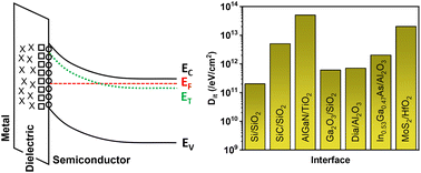
The family of 2-dimensional (2D) semiconductors is a subject of intensive scientific research due to their potential in next-generation electronics. While offering many unique properties like atomic thickness and chemically inert surfaces, the integration of 2D semiconductors with conventional dielectric materials is challenging. The charge traps at the semiconductor/dielectric interface are among many issues to be addressed before these materials can be of industrial relevance. Conventional electrical characterization methods remain inadequate to quantify the traps at the 2D semiconductor/dielectric interface since the estimations of the density of interface traps, Dit, by different techniques may yield more than an order-of-magnitude discrepancy, even when extracted from the same device. Therefore, the challenge to quantify Dit at the 2D semiconductor/dielectric interface is about finding an accurate and reliable measurement method. In this review, we discuss characterization techniques which have been used to study the 2D semiconductor/dielectric interface. Specifically, we discuss the methods based on small-signal AC measurements, subthreshold slope measurements and low-frequency noise measurements. While these approaches were developed for silicon-based technology, 2D semiconductor devices possess a set of unique challenges requiring a careful re-evaluation when using these characterization techniques. We examine the conventional methods based on their efficacy and accuracy in differentiating various types of trap states and provide guidance to find an appropriate method for charge trap analysis and estimation of Dit at 2D semiconductor/dielectric interfaces.
- This article is part of the themed collection: Recent Review Articles
 Please wait while we load your content...

