
 Open Access Article
 This Open Access Article is licensed under a
 Creative Commons Attribution 3.0 Unported Licence
Diblock copolymer pattern protection by silver cluster reinforcement†
Yusuf
Bulut
 ab,
Benedikt
Sochor
a,
Constantin
Harder
ab,
Kristian
Reck
c,
Jonas
Drewes
c,
Zhuijun
Xu
b,
Xiongzhuo
Jiang
b,
Alexander
Meinhardt
de,
Arno
Jeromin
d,
Mona
Kohantorabi
ad,
Heshmat
Noei
ad,
Thomas F.
Keller
de,
Thomas
Strunskus
c,
Franz
Faupel
c,
Peter
Müller-Buschbaum
bf and
Stephan V.
Roth
*ag
ab,
Benedikt
Sochor
a,
Constantin
Harder
ab,
Kristian
Reck
c,
Jonas
Drewes
c,
Zhuijun
Xu
b,
Xiongzhuo
Jiang
b,
Alexander
Meinhardt
de,
Arno
Jeromin
d,
Mona
Kohantorabi
ad,
Heshmat
Noei
ad,
Thomas F.
Keller
de,
Thomas
Strunskus
c,
Franz
Faupel
c,
Peter
Müller-Buschbaum
bf and
Stephan V.
Roth
*ag
aDeutsches Elektronen-Synchrotron DESY, Notkestr. 85, 22607 Hamburg, Germany. E-mail: stephan.roth@desy.de; svroth@kth.se
bTechnical University of Munich, TUM School of Natural Sciences, Department of Physics, Chair for Functional Materials, James-Franck-Str. 1, 85748 Garching, Germany
cChair for Multicomponent Materials, Department of Materials Science, Faculty of Engineering, Christian-Albrechts Universität zu Kiel, Kaiserstr. 2, 24143 Kiel, Germany
dCentre for X-ray and Nano Science CXNS, Deutsches Elektronen-Synchtrotron DESY, Notkestr. 85, 22607 Hamburg, Germany
eDepartment of Physics, University of Hamburg, Notkestr. 9-11, 22607 Hamburg, Germany
fHeinz Maier-Leibnitz Zentrum (MLZ), Technische Universität München, Lichtenbergerstraße 1, 85748 Garching, Germany
gKTH Royal Institute of Technology, Teknikringen 56-58, 100 44 Stockholm, Sweden
First published on 14th September 2023
Abstract
Pattern fabrication by self-assembly of diblock copolymers is of significant interest due to the simplicity in fabricating complex structures. In particular, polystyrene-block-poly-4-vinylpyridine (PS-b-P4VP) is a fascinating base material as it forms an ordered micellar structure on silicon surfaces. In this work, silver (Ag) is applied using direct current magnetron sputter deposition and high-power impulse magnetron sputter deposition on an ordered micellar PS-b-P4VP layer. The fabricated hybrid materials are structurally analyzed by field emission scanning electron microscopy, atomic force microscopy, and grazing incidence small angle X-ray scattering. When applying simple aqueous posttreatment, the pattern is stable and reinforced by Ag clusters, making micellar PS-b-P4VP ordered layers ideal candidates for lithography.
Introduction
Patterned surfaces with the combination of metals and polymers are of vital interest for the fabrication of functional materials and smart sophisticated devices.1–5 Different approaches have evolved to fabricate nanostructured patterns like scanning beam lithography,6 nanoimprint lithography7 and self-assembly.8,9 In particular, self-assembly offers a versatile approach by utilizing diblock copolymers. The material class of diblock copolymers has the property to form ordered morphologies on the nanoscale and to form domains on the same length scale, which is the result of the incompatibility of different blocks (so-called microphase separation).10–12 The size of the nanostructure depends on the polymer block length. The predominant accessible nanostructures obtained with various types of block copolymers are spheres,13,14 relief,15 cylinders,16,17 squares18 and lamellae,19 depending on the block ratio and treatment. Hence, such nanostructured patterns based on soft materials are desired for lithographic applications due to their low cost and simplicity in application.20 These self-assembled patterns may give rise to an alternative route in achieving colloidal lithography compared to the use of polystyrene colloids.21–23 Concerning the use of metals, nanostructured silver (Ag) is of particular interest due to its versatile usage. The optoelectronic properties of Ag on the nanoscale can be exploited in catalysts,24,25 flexible electrodes,26 sensors,27–33 photonic crystals34,35 and antibacterial agents.36,37 Furthermore, it was previously shown that a thin polymer film can be stabilized by the presence of noble metal nanoparticles.38–40 In this work, the focus is on quantitatively evaluating the differences between direct current magnetron sputter deposition (dcMS) and high power impulse magnetron sputter deposition (HiPIMS) of Ag in the stability of polymer based patterns. For the template, a colloidal layer was mimicked by the self-assembly of polystyrene-block-poly-4-vinylpyridine (PS-b-P4VP). The fabrication of an ordered PS-b-P4VP micellar structure was previously shown.13,41,42 The detailed morphology of Ag deposited via dcMS and HiPIMS deposition on the PS-b-P4VP template is investigated by the combination of different characterization techniques: field emission scanning electron microscopy (FESEM), atomic force microscopy (AFM), grazing incidence small angle X-ray scattering (GISAXS) and X-ray reflectometry (XRR). In particular, GISAXS and XRR are powerful techniques providing substantial statistical information of the average structures of the substrate surface.43–45 We show by a simple aqueous washing procedure that the micellar structure is reinforced by dcMS and HiPIMS deposition. Moreover, we show a way to remove the Ag clusters in between the micelles in the case of dcMS, while HiPIMS leads to a more adhesive cluster layer. This offers a new opportunity for a potential water-stable plasmonic hybrid nanostructure.Results and discussion
The nanostructured polystyrene-block-poly-4-vinylpyridine (PS-b-P4VP) micellar film was fabricated through the method adopted by Park et al.13 First, the diblock copolymer PS-b-P4VP was dissolved in toluene under constant stirring at 70 °C for 2 h. As reported, the diblock copolymer forms micelles due to increased solubility of the PS chain in toluene compared to the P4VP. Thus the core of the micelle consists of P4VP and the shell of PS.13 Afterwards, 2 nm Ag was deposited by dcMS and HiPIMS. In Fig. 1(a) the PS-b-P4VP thin micellar diblock copolymer film is seen which is used as spun and forms a well-defined structure. These structures are dimple like structures and show a hexagonal ordering (with some line-type defects), which was previously reported.13 The long range order can be further improved by using a grated silicon wafer followed by THF solvent annealing.41 This can be seen in the FESEM image, Fig. 1a, and the GISAXS pattern (ESI, Fig. S1†). The micelles have an average diameter of d = 51.3 ± 1.9 nm and an average distance of D = 61.2 ± 1.8 nm (see Table 1), derived from the FESEM measurement in Fig. 1(a). Furthermore, the average height of the micellar film is 10.9 ± 1.5 nm which is derived from XRR (Fig. S4†). In Fig. 1(b), an FESEM image of dcMS deposited Ag on top of the PS-b-P4VP micelles (denoted as AgdcMS:PS-b-P4VP) is displayed. It is clearly visible that the Ag clusters on top of the micelles are larger than those in between the micelles (i.e. on the Si surface). Moreover, in Fig. 1(c), the FESEM image of HiPIMS deposited Ag on PS-b-P4VP micelles (denoted as AgHiPIMS:PS-b-P4VP) shows the same behaviour of increased Ag cluster size on the micelles. Furthermore, it is visible that the AgHiPIMS clusters on PS-b-P4VP micelles are smaller compared to the AgdcMS clusters on PS-b-P4VP. The diameter distribution of AgdcMS:PS-b-P4VP deposited Ag nanostructures extracted from two Gaussian fits on top of the micelles yields dS,dcMS,PS-b-P4VP = 4.8 ± 2.1 nm for small nanostructures on the micelles and dS,dcMS,PS-b-P4VP = 14.2 ± 4.4 nm for the large nanostructures on the micelles (Fig. 1d and e). In the case of AgdcMS deposition, the Ag clusters between the micelles again show a bimodal diameter distribution with small and large clusters having a diameter dS,dcMS,Si = 4.6 ± 2.2 nm and dL,dcMS = 11.3 ± 4.5 nm, respectively. In the case of AgHiPIMS:PS-b-P4VP the diameter distribution is described by one monomodal Gaussian distribution with dS,HiPIMS,Pol = 5.8 ± 2.6 nm (Fig. 1f) and thus a smaller dispersity than AgdcMS:PS-b-P4VP. Furthermore, the average diameter distribution of AgHiPIMS:PS-b-P4VP between the micelles has a value of dS,HiPIMS,Si = 5.3 ± 2.2 nm (Fig. 1g). These clusters show a narrower diameter distribution than AgdcMS:PS-b-P4VP between micelles. In both cases, AgHiPIMS:PS-b-P4VP and AgdcMS:PS-b-P4VP deposited Ag forms larger Ag structures on top of the micelles compared to the Ag clusters between the micelles. Furthermore, for Ag clusters with diameter d ≥ 17 nm, the number of AgdcMS:PS-b-P4VP clusters is 20% higher than that of the corresponding AgHiPIMS:PS-b-P4VP clusters. The distribution of AgHiPIMS:PS-b-P4VP is narrower and can be described by one Gaussian distribution in contrast to AgdcMS:PS-b-P4VP. The origin of the monomodal mode for AgHiPIMS:PS-b-P4VP arises from direct implantation of the deposited metal and formation of defects due to the higher ion concentration and their increased kinetic energy. Additionally, these ions are able to form more defects which act as nucleation sites, thus acting as traps limiting the diffusion of atoms and small clusters. Furthermore, it was shown in a study by Lundin et al. comparing dcMS and HiPIMS conditions with regard to kinetic energy distribution that HiPIMS deposited titanium has an increase of kinetic energy distribution which gives rise to a longer diffusion path length.46,47 In the case of dcMS conditions it is expected that the chance of direct implantation is reduced due to the lower kinetic energy distribution and a lower diffusion path length results in the rise of a bimodal distribution, since the coalescence of clusters is not disturbed unlike in the case of the HiPIMS deposition enviroment.32,48 Additionally, atomic force microscopy (AFM) measurements were conducted to obtain height and phase information of the samples.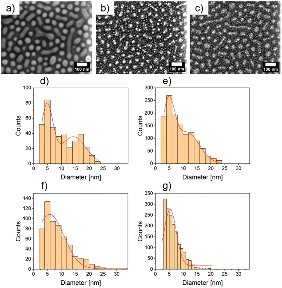 | ||
| Fig. 1 (a) FESEM image of a pristine micellar PS-b-P4VP film. (b) FESEM image of 2 nm dcMS deposited Ag on PS-b-P4VP (AgdcMS:PS-b-P4VP). (c) FESEM image of 2 nm HiPIMS deposited Ag on PS-b-P4VP (AgHiPIMS:PS-b-P4VP). (d) Distribution of AgdcMS:PS-b-P4VP on micelles derived from the FESEM image together with two Gaussian fits. (e) Distribution of AgdcMS:PS-b-P4VP between the micelles derived from the FESEM image together with two Gaussian fits. (f) Distribution of AgHiPIMS:PS-b-P4VP on micelles derived from the FESEM image shown together with a single Gaussian fit. (g) Distribution of AgHiPIMS:PS-b-P4VP between the micelles derived from the FESEM image shown together with a single Gaussian fit. | ||
| Material | Method | Diameter d [nm] | Average distance D [nm] |
|---|---|---|---|
| a S and L denote small and large clusters, respectively. | |||
| PS-b-P4VP | FESEM | 51.3 ± 1.9 | 61.2 ± 1.8 |
| AFM | 49.6 ± 3.2 | 58.3 ± 2.1 | |
| GISAXS | 50.6 ± 7 | 59.2 ± 0.5 | |
| AgdcMS:PS-b-P4VP | FESEM on micelles | 4.8 ± 2.1 (S)a | 13.9 ± 3.9 |
| 14.2 ± 4.4 (L)a | |||
| FESEM between micelles | 4.6 ± 2.2 (S)a | 8.2 ± 2.2 | |
| 11.3 ± 4.5 (L)a | |||
| AFM on micelles | 14.5 ± 3.1 | 17.8 ± 2.6 | |
| GISAXS | — | 6.2 ± 0.2 | |
| AgHiPIMS:PS-b-P4VP | FESEM on micelles | 5.8 ± 2.6 | 12.3 ± 1.8 |
| FESEM between micelles | 5.3 ± 2.2 | 7.7 ± 1.8 | |
| AFM on micelles | 17.2 ± 3.3 | 17.8 ± 1.8 | |
| GISAXS | — | 6.4 ± 0.2 | |
In Fig. 2(a) the height profile of dcMS deposited Ag is displayed. Compared to the FESEM image, the Ag clusters can only be seen on top of the micelles but not in between the micelles in the AFM height image. In the phase image in Fig. 2(b) for AgdcMS:PS-b-P4VP the Ag clusters can be clearly seen on top of the surface of the micelles. The same findings are apparent for the AgHiPIMS:PS-b-P4VP cluster in Fig. 2(d). Moreover, in situ sputter deposition experiments were conducted regarding the real time nanostructure evolution up to a deposited Ag thickness of δAg = 11 nm, which can be found in the ESI (see Fig. S6†). We chose for the investigation δAg = 2 nm deposited AgdcMS:PS-b-P4VP and AgHiPIMS:PS-b-P4VP as they show similar scattering patterns in the GISAXS (see ESI, Fig. S6†) measurements, which indicated that their structural arrangements are similar. In Fig. 3, we present AgdcMS:PS-b-P4VP and AgHiPIMS:PS-b-P4VP GISAXS data proving the structural homogeneity of the Ag cluster and micelle thin film.
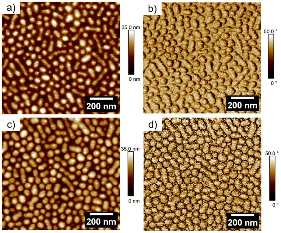 | ||
| Fig. 2 (a) AFM height image of 2 nm dcMS deposited Ag (AgdcMS:PS-b-P4VP). (b) AFM phase image of 2 nm dcMS deposited Ag (AgHiPIMS:PS-b-P4VP). (c) AFM height image of 2 nm HiPIMS deposited Ag (AgdcMS:PS-b-P4VP). (d) AFM phase image of 2 nm HiPIMS deposited Ag (AgHiPIMS:PS-b-P4VP). | ||
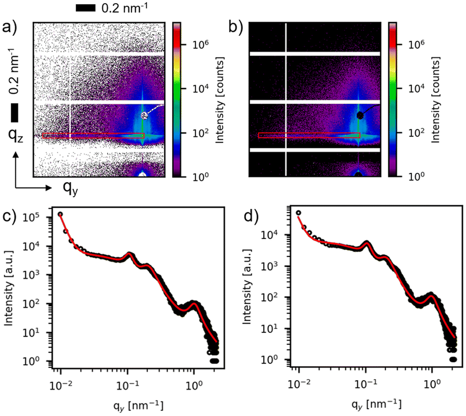 | ||
| Fig. 3 2D GISAXS data of (a) 2 nm dcMS deposited Ag (AgdcMS:PS-b-P4VP) and (b) 2 nm HiPIMS deposited Ag (AgHiPIMS:PS-b-P4VP). A box was added for illustration of the cut position. (c) and (d) The horizontal line cuts of AgdcMS:PS-b-P4VP and AgHiPIMS:PS-b-P4VP, respectively, with the corresponding fit. | ||
In Fig. 3(a and b), two-dimensional (2D) GISAXS patterns are displayed corresponding to a deposited Ag thickness of δAg = 2 nm for both AgdcMS:PS-b-P4VP and AgHiPIMS:PS-b-P4VP. GISAXS yields high average statistical information of the nanostructures in the thin film, as it probes a larger area compared to FESEM and AFM due to the enlarged footprint in the beam direction. Moreover, in order to obtain structural information on the distance of the nanostructures, horizontal line cuts are performed as indicated by the red box as the region of interest (Fig. 3a and b). The horizontal cut from the detector image is performed at the height of the critical angle of silicon (αSi = 0.15 ± 0.01°) as this contains the highest intensity of the desired structural information. These horizontal line cuts are displayed in Fig. 3(c) and (d). The pronounced domain peaks are visible in the GISAXS pattern (see ESI, Fig. S1†). A simplified model was constructed to fit the data with a set of Lorentzian function as the structure factor and a cylindrical form factor for the patterned polymer template to obtain the desired structural information of the sample. The Ag structure peak is visible at qy,dcMS,max = 1.01 ± 0.02 nm−1 for AgdcMS:PS-b-P4VP, whereas for AgHiPIMS:PS-b-P4VP qy,HiPIMS,max = 0.98 ± 0.02 nm−1, which is obtained by the model applied as a fit (Fig. 3c and d). The average distance can be calculated as d ≈ 2πqy,max−1. For AgdcMS:PS-b-P4VP we obtained an average distance of ddcMS = 6.2 ± 0.2 nm and for AgHiPIMS:PS-b-P4VP the average distance was dHiPIMS = 6.4 ± 0.2 nm.
Furthermore, the XPS spectra of AgdcMS:PS-b-P4VP (Fig. 4a) and AgHiPIMS:PS-b-P4VP (Fig. 4b) were measured and they showed that the silver clusters are identical in their chemical environment. In addition, no change in the C 1s, N 1s and O 1s edge is observable between pristine, AgdcMS:PS-b-P4VP and AgHiPIMS:PS-b-P4VP (see ESI, Fig. S7†). The structure and chemical characterization show that for AgdcMS:PS-b-P4VP and AgHiPIMS:PS-b-P4VP the optimal starting conditions are met for the comparison of both deposition techniques.
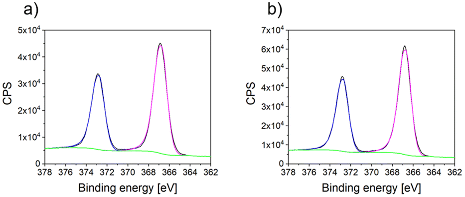 | ||
| Fig. 4 (a) XPS spectra at the Ag 3d edge of AgdcMS:PS-b-P4VP and (b) XPS spectra at the Ag 3d edge of AgHiPIMS:PS-b-P4VP together with a Gaussian fit. | ||
In Fig. 5(a) the surface energy is displayed which was derived using ultrapure water on pristine PS-b-P4VP, AgdcMS:PS-b-P4VP and AgHiPIMS:PS-b-P4VP. The procedure was to initially place a droplet (10 μL) on top of the surface and measure directly the contact angle. Afterwards, the droplets dried under ambient conditions on the surface with a duration of approximately 1.5 h. In the case of the pristine PS-b-P4VP micellar film, the surface energy is at 19.5 ± 0.7 mN m−1 having a hydrophilic character. After the first droplet dried, FESEM measurements (Fig. 5b) were conducted which showed a partial degradation of the micellar film. In comparison, AgdcMS:PS-b-P4VP becomes hydrophobic with a surface energy of 10.5 ± 0.5 mN m−1, which is also observed for Ag nanoparticles being hydrophobic solutes in solution.49 After drying of a water droplet, the FESEM measurement (Fig. 5c) of AgdcMS:PS-b-P4VP reveals that a partial delamination of the Ag clusters on top of the Si substrate occurs, which is observable within the red circled region. However, Ag clusters, which had grown on top of the micelles, stayed intact and stabilized the micellar film. In addition, the AgHiPIMS:PS-b-P4VP hybrid thin film has a surface energy of 9.5 ± 0.4 mN m−1 which renders this hybrid layer slightly more hydrophobic than AgdcMS:PS-b-P4VP.
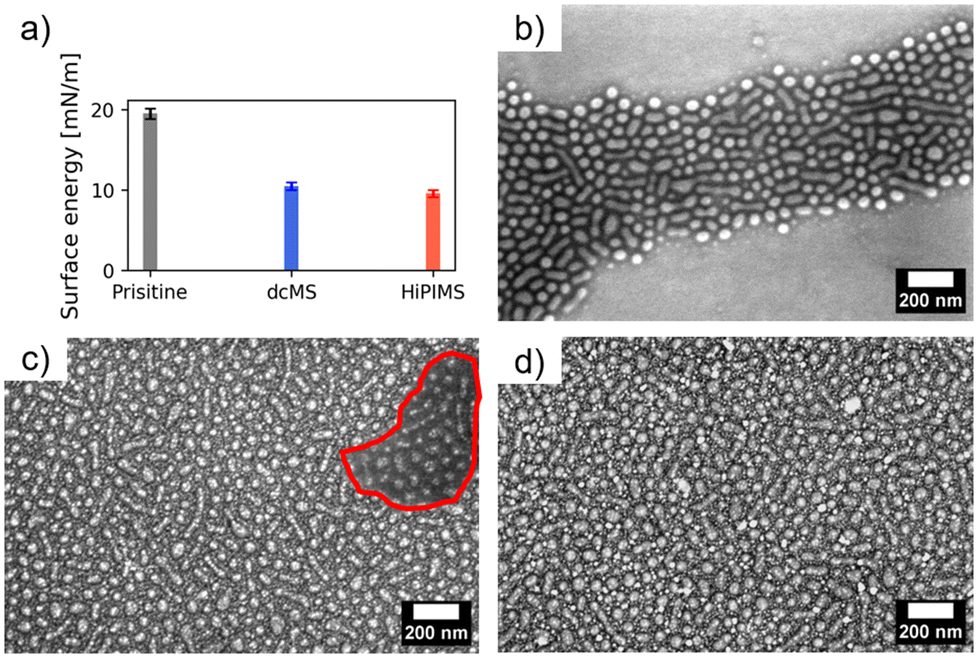 | ||
| Fig. 5 (a) Contact angle measurements of water droplets on the surface of pristine PS-b-P4VP, AgdcMS:PS-b-P4VP and AgHiPIMS:PS-b-P4VP. (b) The FESEM image of the pristine PS-b-P4VP after 1 dried water droplet and (c) the FESEM image of AgdcMS:PS-b-P4VP after 1 droplet dried. The red circle indicates the area in which Ag clusters were removed from the substrate. (d) The FESEM image of AgHiPIMS:PS-b-P4VP after drying of one water droplet. | ||
Upon drying of the first water droplet, it is clearly visible in the FESEM images that the micellar film with the Ag structures on the micelles and the Ag structures between the micelles remains intact after the aqueous treatment. Both deposition techniques are able to provide a reinforcement of the micellar structure.
The second approach for the aqueous treatment was placing a 10 μL water droplet on top of the substrate surface and absorbing it immediately with a tissue paper (Kimtech, USA) to remove excess solvent or to dry surfaces before conducting contact angle measurements following previously published procedures.50,51 This procedure was performed 5 times on AgdcMS:PS-b-P4VP and AghiPIMS:PS-b-P4VP. After the treatment, AgdcMS:PS-b-P4VP shows that large agglomerations of Ag clusters emerged (Fig. 6a). Upon magnification (Fig. 6b), it is clearly visible that AgdcMS:PS-b-P4VP clusters agglomerated indeed into large Ag structures beforehand. Clusters between the micelles in AgdcMS:PS-b-P4VP and to some extent some on top of the micelles are removed and thus these large Ag agglomerations are formed, which is schematically represented in Fig. 6(e). The lithographic pattern formed by PS-b-P4VP micelles and the deposited Ag remain intact. The micellar layer dictates the precise positioning or anchoring of the Ag clusters, as the majority of the residual clusters were delaminated off the silicon substrate. The origin of this delamination is expected to be the lack of direct implantation on the silicon wafer and partially on the diblock copolymer.47 Furthermore the origin of the Ag agglomeration is the close distance of the clusters which are not protected by any agent preventing that.52 This shows that a prepatterned substrate can retain the deposited micellar pattern in its original position when using dcMS deposition of Ag. In contrast, AgHiPIMS:PS-b-P4VP shows no such large agglomeration after the aqueous treatment (Fig. 6c). Even in the magnified FESEM image (Fig. 6d), AgHiPIMS:PS-b-P4VP structures remain intact after aqueous treatment, which is schematically presented in Fig. 6(f). This shows that upon Ag HiPIMS deposition, the clusters on AgHiPIMS:PS-b-P4VP are much more stable upon treatment, which shows their potential to be used in aqueous environments for SERS sensing.53 Since the structure and chemical environment of AgdcMS:PS-b-P4VP and AgHiPIMS:PS-b-P4VP are similar, eventually lattice defects in the cluster structure are responsible for the different behaviour upon aqueous treatment. AgHiPIMS:PS-b-P4VP has less defects compared to AgdcMS:PS-b-P4VP, since HiPIMS deposited films are in general denser than dcMS deposited films, thus hindering the dewetting of the Ag clusters of the substrate. This shows the great potential of PS-b-P4VP micelles for being a water stable advanced hybrid material for advanced plasmonic devices.54,55
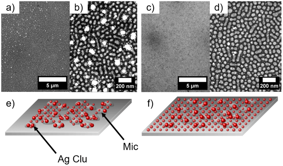 | ||
| Fig. 6 (a) Overview FESEM image of AgdcMS:PS-b-P4VP after aqueous treatment and (b) FESEM image of AgdcMS:PS-b-P4VP after aqueous treatment, (c) overview of the FESEM image of AgHiPIMS:PS-b-P4VP after aqueous treatment and (d) FESEM image of AgHiPIMS:PS-b-P4VP after aqueous treatment. (e) Schematic representation of the removal of silver clusters of AgdcMS:PS-b-P4VP between the micelles and (f) schematic representation of the stable AgdcMS:PS-b-P4VP after aqueous treatment. ‘Mic’ denotes to micelles and ‘Ag Clu’ denotes Ag clusters. | ||
Experimental
Materials
Silicon wafer (Si-Mat Silicon Materials, Germany) was cut into pieces with a size of 12 × 15 mm2 and cleaned in an acidic bath containing sulfuric acid and hydrogen peroxide at 70 °C for 15 minutes. After the acidic bath cleaning procedure, the silicon pieces were heavily rinsed with ultra-pure water to remove any acidic acid content and stored in an ultrapure water bath. The polymer polystyrene-b-poly-4-vinylpyridine (PS-b-P4VP, Mn = 35.0 kg mol−1-b-21.0 kg mol−1, PDI = 1.09) was supplied by Polymer Source, Canada. PS-b-P4VP was dissolved in toluene (Sigma-Aldrich, Germany) with a concentration of 4.3 mg mL−1. The polymeric solution was heat treated for 2 h at 70 °C.Polymer film preparation
The cleaned silicon pieces were removed from the storage bath and rinsed with ultrapure water. Afterwards, the silicon pieces were blown dry under a nitrogen steam. The dried silicon pieces were loaded into an M-SPIN 200 Spin Coater (Ramgraber GmbH, Germany). The PS-b-P4VP film preparation was adapted from Park et al.13 with a setting of 60 s at 2000 rpm and an acceleration of 100%. The spincast polymer films were used as spun in the following experiments.Physical vapor deposition
The sputter chamber is a self-built sputter deposition chamber which was described in a previous article.48 For all experiments, sputtering of silver (Ag, Kurt J. Lesker) from a two inch target was performed with the following sputter parameters. The dynamic working pressure was pAr = 0.36 Pa with an argon flow of 10 sccm. For dcMS the average power was P = 23 W and the discharge voltage was U = 310 ± 4 V. For HiPIMS the pulse length was 20 μs with a frequency of 150 Hz. A discharge voltage of U = 952 ± 4 V resulted in a peak current density of I = 1.41 ± 0.13 A cm−2. The average power was set to P = 40 W to achieve the same deposition rate as for dcMS. The deposition rates were determined with a quartz crystal microbalance (QCM), being 0.222 ± 0.006 nm s−1 for HiPIMS and dcMS. The QCM results were verified with a profilometer.Field emission scanning electron microscopy
High resolution field emission scanning electron microscopy (FESEM) images were taken with a Nova NanoSEM 450 (FEI Thermo Fisher).56 ImageJ was used to visualize the measured FESEM images and to obtain statistical information about the size of the silver cluster. Afterwards, the obtained dataset was binned and plotted with the software Origin. The average distance between clusters was estimated manually by analysing 50 cluster–cluster distances (ESI, Fig. S2†). The same procedure was used for the micelle–micelle distance and the micelle diameter (ESI, Fig. S3†).Atomic force microscopy
Atomic force microscopy (AFM) measurements were performed in the intermittent tapping mode with RTESPA-150 Cantilevers. Furthermore, a Bruker (Dimension Icon equipped with a NanoScope V controller) AFM was used for the measurement. The AFM images were chosen to be 2 μm × 2 μm with a scan rate of 0.5 Hz and a resolution of 1024 × 1024 pixel. NanoScope Analysis software was used for visualization of the measurements.56 The distance between the micellar structures, the distance between the Ag clusters, the diameter of the micellar structure and the diameter of the Ag cluster were measured manually 50 times at different positions of the image to obtain statistical information (ESI, Fig. S4†). The average distance between clusters was calculated from manually analysed 50 cluster–cluster distances and cluster diameters. The same procedure was applied for the micelle–micelle distance and the micelle diameter (ESI, Fig. S4†).Contact angle
Contact angle measurements were performed with an OCA 35 (Dataphysics). The water droplet size was 10 μL. Derived from the contact angle, the surface energy was calculated (see the ESI†).57–59Grazing incidence small angle X-ray scattering and X-ray reflectometry
The grazing incidence small angle X-ray scattering (GISAXS) and X-ray reflectometry (XRR) experiments were performed at P03/PETRA III at DESY (Hamburg, Germany), with a custom made deposition chamber as previously reported.48 The chamber was upgraded with a guard blade to reduce background. A point shape beam (30 μm × 25 μm) was used with the incident angle being αi = 0.4°. The distance of the Pilatus 2M (Dectris Ltd, Switzerland) to the sample (SDD) was set to SDD = 3415 ± 2 mm. The photon energy was chosen to be 11.8 keV. The pixel size of one pixel is 172 μm × 172 μm. The XRR data were analyzed with MOTOFIT 0.1.20 (ESI, Fig. S5†).60X-ray photoelectron spectroscopy
The core-level photoelectron spectra of the as-prepared samples were measured by X-ray photoelectron spectroscopy (XPS) at DESY Nanolab using a monochromated Al Kα source (1.4 keV) and a Phoibos 150 hemispherical energy analyzer.56 The flood gun was used during the XPS measurements at an energy 2.0 eV with 20 μA emission.Conclusions
The structural and functional properties of PS-b-P4VP micellar films with AgdcMS:PS-b-P4VP and AgHiPIMS:PS-b-P4VP coated Ag hybrid structures for application in patterned surfaces with potential for lithography were investigated. Our study reveals that the Ag cluster arrangement is homogeneous on the diblock micellar pattern surface. Moreover, the Ag clusters being located on top of the micelles have an average larger size than the Ag clusters between the micelles. Furthermore, AgdcMS:PS-b-P4VP produces slightly larger clusters on the micelles than AgHiPIMS:PS-b-P4VP deposited Ag. AFM reveals that the Ag clusters grow on the surface of the micelles. GISAXS confirms that the structural arrangement is homogeneous throughout the sample. Upon an aqueous treatment, the pristine, nanostructured PS-b-P4VP micellar film partially rearranges. Depositing Ag on the micellar film reinforces or stabilizes the PS-b-P4VP micellar structure, a necessary requirement for the aqueous treatment. Furthermore, in the case of dcMS, the Ag clusters are partially washed away after an aqueous treatment compared to HiPIMS deposited Ag clusters which originates from an increased adhesion due to this novel deposition technique.47 Thus, these results impact the tailoring of protective layers for complex structured polymer-based templates.Conflicts of interest
There are no conflicts to declare.Acknowledgements
This work was partially funded by the Deutsche Forschungsgemeinschaft (DFG, German Research Foundation) – project 459798762 (RO 4638/3-1, FA 234/36-1, and MU 1487/39-1). C. H. acknowledges funding from the DESY innovation fund. We acknowledge DESY (Hamburg, Germany), a member of the Helmholtz Association HGF, for the provision of experimental facilities. Parts of this research were carried out at PETRA III and at the DESY NanoLab and we would like to thank Jan Rubeck for assistance in using P03. Beamtime was allocated for proposal I-20220548.References
- B. Zhang, L. Meng and Z. Li, RSC Adv., 2022, 12, 28376–28387 RSC.
- K. V. Sarathlal, D. Kumar and A. Gupta, Appl. Phys. Lett., 2011, 98, 2009–2012 Search PubMed.
- H. Walter and A. Leitner, Opt. Eng., 2006, 45, 103801 CrossRef.
- L. Guo, W. Liu and C. Wang, ACS Appl. Nano Mater., 2023, 6, 7830–7840 CrossRef CAS.
- A. P. Shah, S. Jain and N. G. Shimpi, ChemistrySelect, 2020, 5, 3897–3905 CrossRef CAS.
- A. Haider, M. Yilmaz, P. Deminskyi, H. Eren and N. Biyikli, RSC Adv., 2016, 6, 106109–106119 RSC.
- P. Yi, C. Zhang, L. Peng and X. Lai, RSC Adv., 2017, 7, 48835–48840 RSC.
- D. S. Jung, J. Bang, T. W. Park, S. H. Lee, Y. K. Jung, M. Byun, Y. R. Cho, K. H. Kim, G. H. Seong and W. I. Park, Nanoscale, 2019, 11, 18559–18567 RSC.
- T. S. Dörr, A. Pelz, P. Zhang, T. Kraus, M. Winter and H. D. Wiemhöfer, Chem. – Eur. J., 2018, 24, 8061–8065 CrossRef PubMed.
- A. Cho, Y. La, S. Jeoung, H. R. Moon, J. Ryu and T. J. Shin, Macromolecules, 2017, 50, 3234–3243 CrossRef CAS.
- T. P. Le, B. H. Smith, Y. Lee, J. H. Litofsky, M. P. Aplan, B. Kuei, C. Zhu, C. Wang, A. Hexemer and E. D. Gomez, Macromolecules, 2020, 53, 1967–1976 CrossRef CAS.
- D. Wi, J. Kim, H. Lee, N. G. Kang, J. Lee, M. J. Kim, J. S. Lee and M. Ree, J. Mater. Chem. C, 2016, 4, 2017–2027 RSC.
- S. Park, J. Y. Wang, B. Kim, W. Chen and T. P. Russell, Macromolecules, 2007, 40, 9059–9063 CrossRef CAS.
- R. Mezzenga, J. Ruokolainen and A. Hexemer, Langmuir, 2003, 19, 8144–8147 CrossRef CAS.
- P. Zhang, Z. Wang, H. Huang and T. He, Macromolecules, 2012, 45, 9139–9146 CrossRef CAS.
- M. Gensch, M. Schwartzkopf, C. J. Brett, S. J. Schaper, L. P. Kreuzer, N. Li, W. Chen, S. Liang, J. Drewes, O. Polonskyi, T. Strunskus, F. Faupel, P. Müller-Buschbaum and S. V. Roth, ACS Appl. Nano Mater., 2021, 4, 4245–4255 CrossRef CAS.
- M. Park, C. Harrison, P. M. Chaikin, R. A. Register and D. H. Adamson, Science, 1997, 276, 1401–1404 CrossRef CAS.
- C. Tang, E. M. Lennon, G. H. Fredrickson, E. J. Kramer and C. J. Hawker, Science, 2008, 322, 429–432 CrossRef CAS PubMed.
- A. V. Berezkin, F. Jung, D. Posselt, D. Smilgies and C. M. Papadakis, Adv. Funct. Mater., 2018, 28, 1706226 CrossRef.
- Z. Qiang, S. A. Akolawala and M. Wang, ACS Macro Lett., 2018, 7, 566–571 CrossRef CAS PubMed.
- B. Ai, H. Möhwald, D. Wang and G. Zhang, Adv. Mater. Interfaces, 2017, 4, 1600271 CrossRef.
- S. Krishnamoorthy, M. A. F. Van Den Boogaart, J. Brugger, C. Hibert, R. Pugin, C. Hinderling and H. Heinzelmann, Adv. Mater., 2008, 20, 3533–3538 CrossRef CAS.
- S. S. Shankar, L. Rizzello, R. Cingolani, R. Rinaldi and P. P. Pompa, ACS Nano, 2009, 3, 893–900 CrossRef CAS PubMed.
- Y. Liu, X. Chai, X. Cai, M. Chen, R. Jin, W. Ding and Y. Zhu, Angew. Chem., Int. Ed., 2018, 57, 9775–9779 CrossRef CAS PubMed.
- Z. Chang, X. Jing, C. He, X. Liu and C. Duan, ACS Catal., 2018, 8, 1384–1391 CrossRef CAS.
- R. T. Piper, W. Xu and J. W. P. Hsu, MRS Adv., 2023, 177–182 CrossRef CAS.
- C. Tsao, Y. Zheng, Y. Sun and Y. Cheng, Analyst, 2021, 146, 7645–7652 RSC.
- J. N. Anker, W. P. Hall, O. Lyandres, N. C. Shah, J. Zhao and R. P. Van Duyne, Nat. Mater., 2008, 7, 8–10 CrossRef PubMed.
- L. J. Sherry, S.-H. Chang, G. C. Schatz, R. P. Van Duyne, B. J. Wiley and Y. Xia, Nano Lett., 2005, 5, 2034–2038 CrossRef CAS PubMed.
- J. Alegret, T. Rindzevicius, T. Pakizeh, Y. Alaverdyan, L. Gunnarsson and M. Käll, J. Phys. Chem. C, 2008, 112, 14313–14317 CrossRef CAS.
- M. Gensch, M. Schwartzkopf, W. Ohm, C. J. Brett, P. Pandit, S. K. Vayalil, L. Bießmann, L. P. Kreuzer, J. Drewes, O. Polonskyi, T. Strunskus, F. Faupel, A. Stierle, P. Müller-Buschbaum and S. V. Roth, ACS Appl. Mater. Interfaces, 2019, 11, 29416–29426 CrossRef CAS PubMed.
- F. Faupel, V. Zaporojtchenko, T. Strunskus and M. Elbahri, Adv. Eng. Mater., 2010, 12, 1177–1190 CrossRef CAS.
- U. Schürmann, W. Hartung, H. Takele, V. Zaporojtchenko and F. Faupel, Nanotechnology, 2005, 16, 1078–1082 CrossRef.
- X. Cao, Y. Xiao, Q. Dong, S. Zhang, J. Wang, L. Wang and L. Gao, Adv. Photonics Res., 2022, 3, 2200127 CrossRef CAS.
- W. Wang and S. A. Asher, J. Am. Chem. Soc., 2001, 123, 12528–12535 CrossRef CAS PubMed.
- K. Zheng and J. Xie, Acc. Mater. Res., 2021, 2, 1104–1116 CrossRef CAS.
- I. Chakraborty, T. Udayabhaskararao, G. K. Deepesh and T. Pradeep, J. Mater. Chem. B, 2013, 1, 4059–4064 RSC.
- G. Amarandei, C. O'Dwyer, A. Arshak and D. Corcoran, ACS Appl. Mater. Interfaces, 2013, 5, 8655–8662 CrossRef CAS PubMed.
- G. Amarandei, I. Clancy, C. O'Dwyer, A. Arshak and D. Corcoran, ACS Appl. Mater. Interfaces, 2014, 6, 20758–20767 CrossRef CAS PubMed.
- G. Amarandei, C. O'Dwyer, A. Arshak and D. Corcoran, Soft Matter, 2013, 9, 2695–2702 RSC.
- S. Park, B. Kim, O. Yavuzcetin, M. T. Tuominen and T. P. Russell, ACS Nano, 2008, 2, 1363–1370 CrossRef CAS PubMed.
- H. Y. Si, J. S. Chen and G. M. Chow, Colloids Surf., A, 2011, 373, 82–87 CrossRef CAS.
- S. V. Roth, G. Santoro, J. F. H. Risch, S. Yu, M. Schwartzkopf, T. Boese, R. Döhrmann, P. Zhang, B. Besner, P. Bremer, D. Rukser, M. A. Rübhausen, N. J. Terrill, P. A. Staniec, Y. Yao, E. Metwalli and P. Müller-Buschbaum, ACS Appl. Mater. Interfaces, 2015, 7, 12470–12477 CrossRef CAS PubMed.
- S. J. Schaper, F. C. Löhrer, S. Xia, C. Geiger, M. Schwartzkopf, P. Pandit, J. Rubeck, B. Fricke, S. Frenzke, A. M. Hinz, N. Carstens, O. Polonskyi, T. Strunskus, F. Faupel, S. V. Roth and P. Müller-Buschbaum, Nanoscale, 2021, 13, 10555–10565 RSC.
- S. V. Roth, H. Walter, M. Burghammer, C. Riekel, B. Lengeler, C. Schroer, M. Kuhlmann, T. Walther, A. Sehrbrock, R. Domnick and P. Müller-Buschbaum, Appl. Phys. Lett., 2006, 88, 1–3 CrossRef.
- D. Lundin, P. Larsson, E. Wallin, M. Lattemann, N. Brenning and U. Helmersson, Plasma Sources Sci. Technol., 2008, 17, 035021 CrossRef.
- R. Bandorf, S. Waschke, F. C. Carreri, M. Vergöhl, G. Grundmeier and G. Bräuer, Surf. Coat. Technol., 2016, 290, 77–81 CrossRef CAS.
- M. Schwartzkopf, A. Hinz, O. Polonskyi, T. Strunskus, F. C. Löhrer, V. Körstgens, P. Müller-Buschbaum, F. Faupel and S. V. Roth, ACS Appl. Mater. Interfaces, 2017, 9, 5629–5637 CrossRef CAS PubMed.
- R. S. Cataliotti, F. Aliotta and R. Ponterio, Phys. Chem. Chem. Phys., 2009, 11, 11258–11263 RSC.
- S. Singha, V. Gowda and M. S. Hedenqvist, ACS Appl. Polym. Mater., 2021, 3, 4088–4100 CrossRef CAS.
- Z. Zhang, J. L. Wilson, B. R. Kitt and D. W. Flaherty, ACS Appl. Polym. Mater., 2021, 3, 986–995 CrossRef CAS.
- A. Pyatenko, K. Shimokawa, M. Yamaguchi, O. Nishimura and M. Suzuki, Appl. Phys. A: Mater. Sci. Process., 2004, 79, 803–806 CrossRef CAS.
- C. Zhang, S. Chen, Z. Jiang, Z. Shi, J. Wang and L. Du, ACS Appl. Mater. Interfaces, 2021, 13, 29222–29229 CrossRef CAS PubMed.
- A. Issa, I. Izquierdo, M. Merheb, D. Ge, A. Broussier, N. Ghabri, S. Marguet, C. Couteau, R. Bachelot and S. Jradi, ACS Appl. Mater. Interfaces, 2021, 13, 41846–41856 CrossRef CAS PubMed.
- T. J. Wang, N. R. Barveen, Z. Y. Liu, C. H. Chen and M. H. Chou, ACS Appl. Mater. Interfaces, 2021, 13, 34910–34922 CrossRef CAS PubMed.
- H. Noei, V. Vonk, T. F. Keller, R. Roehlsberger and A. Stierle, J. Large-Scale Res. Facil., 2016, 2, 1–9 Search PubMed.
- N. B. Vargaftik, B. N. Volkov and L. D. Voljak, J. Phys. Chem. Ref. Data, 1983, 12, 817–820 CrossRef CAS.
- P. G. De Gennes, Rev. Mod. Phys., 1985, 57, 827–863 CrossRef CAS.
- R. J. Good and L. A. Girifalco, J. Phys. Chem., 1960, 64, 561–565 CrossRef CAS.
- A. R. J. Nelson and S. W. Prescott, J. Appl. Crystallogr., 2019, 52, 193–200 CrossRef CAS PubMed.
Footnote |
| † Electronic supplementary information (ESI) available. See DOI: https://doi.org/10.1039/d3nr03215a |
| This journal is © The Royal Society of Chemistry 2023 |