
 Open Access Article
 This Open Access Article is licensed under a
 Creative Commons Attribution 3.0 Unported Licence
Evaluating strain and doping of Janus MoSSe from phonon mode shifts supported by ab initio DFT calculations†
Jennifer
Schmeink
 ,
Vladislav
Musytschuk
,
Erik
Pollmann
,
Stephan
Sleziona
,
André
Maas
,
Peter
Kratzer
and
Marika
Schleberger
*
,
Vladislav
Musytschuk
,
Erik
Pollmann
,
Stephan
Sleziona
,
André
Maas
,
Peter
Kratzer
and
Marika
Schleberger
*
University of Duisburg-Essen, Faculty of Physics and CENIDE, 47057 Duisburg, Germany. E-mail: marika.schleberger@uni-due.de
First published on 12th June 2023
Abstract
With the study of Janus monolayer transition metal dichalcogenides, in which one of the two chalcogen layers is replaced by another type of chalcogen atom, research on two-dimensional materials is advancing into new areas. Yet only little is known about this new kind of material class, mainly due to the difficult synthesis. In this work, we synthesize MoSSe monolayers from exfoliated samples and compare their Raman signatures with density functional theory calculations of phonon modes that depend in a nontrivial way on doping and strain. With this as a tool, we can infer limits for the possible combinations of strain and doping levels. This reference data can be applied to all MoSSe Janus samples in order to quickly estimate their strain and doping, providing a reliable tool for future work. In order to narrow down the results for our samples further, we analyze the temperature-dependent photoluminescence spectra and time-correlated single-photon counting measurements. The lifetime of Janus MoSSe monolayers exhibits two decay processes with an average total lifetime of 1.57 ns. Moreover, we find a strong trion contribution to the photoluminescence spectra at low temperature which we attribute to excess charge carriers, corroborating our ab initio calculations.
1. Introduction
Since the discovery of graphene in 2004, the field of two dimensional (2D) materials has matured and virtually dozens of 2D materials have been synthesized and characterized. The search for more versatile 2D materials has recently led to the successful synthesis of so-called Janus-type 2D materials1–3 based on transition metal dichalcogenide (TMDC) monolayers. Those are comprised of a TMDC where the chalcogen atoms on one side of the monolayer are substituted by another type of chalcogen atoms, typically denoted as MXY (M = Mo, W, …; X, Y = S, Se, Te, X ≠ Y), see Fig. 1(a) and (b). | ||
| Fig. 1 Structure and fabrication of Janus monolayers. (a) Top- and (b) side-view of a Janus-type TMDC. Transition metal atoms (purple) are sandwiched between two layers of different chalcogen atoms (yellow & orange). (c) Schematic illustration of the thermal sulfurization process. Depicted are two heating zones of a tube furnace. The sulfur source and the exfoliated substrates are located in different, thermally isolated parts in the oven. Argon gas is inserted into the quartz tube coming from the left. The inset shows simplified the replacement of atoms during the thermal processing. | ||
The top and bottom layer are thus made up from elements with different electronegativity which leads to a built-in electrical field within the Janus layer so that the mirror symmetry of the conventional MX2 TMDC is broken, resulting in completely different physical properties.4–6 These Janus-type group-VI TMDC monolayers are predicted to be semiconductors, to preserve spin splitting at band edges and thus valley properties, to possess a large momentum dependent spin splitting (Rashba effect) due to the spontaneous out-of-plane dipole and an intrinsic in-plane piezoelectric effect.7–10 Furthermore, the structural asymmetry along the out-of-plane direction enables efficient charge separation rendering the Janus TMDC monolayer attractive for photovoltaics and photocatalysis alike.11–13 2D layers of this type were already predicted to be stable in 201314 but the synthesis of a Janus MoSSe monolayer was experimentally realized in 20171,2 and the number of different Janus materials synthesized since then has remained strikingly low.15
The synthesis protocols reported so far, ranging from different kinds of plasma etching,1,16–19 over pulsed laser deposition,20 to simple thermal etching in a chalcogen rich atmosphere,2 have mostly been using a base material that was grown via chemical vapor deposition (CVD). However, Qin et al. recently established the use of exfoliated samples as the base material for synthesizing Janus monolayers via an in situ, deterministic growth process.21
These various preparation schemes result in intricate differences in the end product as the quality of bulk materials in terms of structure often exceeds that of CVD materials. The latter are usually prone to intrinsic defects22–24 and they typically exhibit a stronger interaction with the substrate leading to increased strain and doping.25,26
Strain and doping are important properties but are oftentimes difficult to measure directly, thus a reliable workaround is needed for their evaluation. By correlating the phonon frequencies of a material with the calculated values for strain and doping, one can derive isometric dependencies, which serve as a fast and simple tool for a decoupling and quantification by optical spectroscopy. This approach, i.e. plotting the Raman shifts as a function of strain and charge carrier density, has already been proven exceptionally useful for graphene (2D vs. G plots by Lee et al.27) and for MoS2 (E vs. A plots by Michail et al.28), but is not yet available for Janus 2D materials.
In this work, we aim to provide such a correlation plot as a reference for future work in this field. To this end, we synthesize Janus MoSSe from exfoliated MoSe2 with a fabrication method akin to Zhang et al.2 and by comparing the Raman signature with our ab initio calculations we evaluate the sample's strain and doping. We show that the reference plot for Janus MoSSe is more complex than in the case of graphene and MoS2. More specifically, the correlations turn out to be non-linear, and thus additional information is needed to distinguish between the two possible combinations of strain and doping. In our case, the analysis of the excitonic properties allows us to infer the strain and doping of our samples.
2. Results and discussion
2.1. Fabrication of Janus MoSSe
We start by briefly describing our basic setup that is schematically shown in Fig. 1(c). We use a multi zone tube furnace to thermally etch exfoliated MoSe2 samples in a sulfur rich environment. For more details see the method section. This approach works best with a selenium based material such as MoSe2 because Se-bonds are weaker than S-bonds due to the weaker electronegativity and the more delocalized electronic structure.29Before thermal processing, the monolayer regions of the exfoliated MoSe2 samples are identified by atomic force microscopy as will be shown further down. The fastest method to ensure that the transformation process was successful is to inspect the samples’ Raman and photoluminescence (PL) signatures. As shown in Fig. 2(a), the Raman signature of the Janus monolayer (blue) is distinctively different for the two base TMDCs MoS2 (green) and MoSe2 (red). All three materials show thetypical in- and out-of-plane vibrational modes, denoted E12g and A1g, respectively. As can be seen from the MoSSe spectrum, there are no remnants of the MoSe2- nor MoS2-modes. Therefore, the blue spectrum stems from an ideal Janus MoSSe monolayer with its A1g-mode at 289 cm−1 and its E12g-mode at 352 cm−1. These values are in good agreement with both, other experimental data1,2 and theoretical results.13,19,30
 | ||
| Fig. 2 Successful preparation of a 2D Janus material starting from MoSe2 exfoliated onto SiO2. Normalized (a) Raman-spectra with 532 nm laser excitation and (b) low temperature photoluminescence-spectra at 77 K comparison of the exfoliated base TMDCs: MoS2 (green) and MoSe2 (red), with the Janus monolayer MoSSe (blue). Raman spectra taken in the monolayer region show the characteristic A1g and E12g modes of MoSe2. After thermal processing of an MoSe2 sample in an S-rich atmosphere its Raman modes shift, indicating the successful transformation into Janus MoSSe. | ||
The strong PL signals from MoSe2 and MoS2, see Fig. 2(b), are by themselves a sign for the material being a monolayer, as they occur due to the shift from an indirect to a direct band gap when the materials are thinned down. Moreover, the energies of the two PL-peaks correspond to the so called A- and B-exciton transition energies. For MoS2 these transition energies at 77 K are 1.84 eV and 2.04 eV, and for MoSe2 at 77 K we find 1.59 eV and 1.80 eV for A- and B-excitons, respectively. As expected, the PL of a MoSSe monolayer lies energetically right in between those of MoS2 and MoSe2, with an A-exciton transition energy of 1.75 eV and a B-exciton of 1.93 eV at 77 K. These values are consistent with prior experimental1,2 and theoretical predictions.7,13,31 The full width at half maximum (FWHM) of the A-exciton in the photoluminescence spectra are furthermore an indication of quality as the peak widens with impurities. The exfoliated MoSe2 exhibits the smallest FWHM at 77 K at 49 meV, MoS2's is 69 meV and the Janus MoSSe's width is 73 meV. Previous work on MoSSe has reported similar widths.32 That the FWHM does not differ too much from the exfoliated TMDCs is a sign that the quality of our sample even after processing is still very good. Therefore, the PL can serve as a further confirmation of the successful transformation of a MoSe2 monolayer into a Janus-type MoSSe monolayer.
2.2. DFT calculations of strain and doping dependent phonon mode shifts
As discussed above, the exact energy of the Raman active phonon modes is very important in terms of evaluating the quality of the Janus monolayer. However, their energy can shift due to additional factors. Such factors include the intrinsic and extrinsic doping of the material, and the strain of the flake. To identify the dependence of these factors and the phonon mode shifts we use density functional theory (DFT). For a detailed explanation of the calculation parameters, code, and approximations used we refer the reader to the Methods section. The resulting calculations correlate the Raman shifts of the A1g and E12g phonon modes of MoSSe with both, induced strain and doping of the monolayer. The calculated frequencies shift non-linearly with variable strain and doping levels, as visualised in Fig. 3(a) for the A1g- and in (b) for the E12g-mode. | ||
| Fig. 3 Density functional theory calculations of phonon mode shifts with variable strain and doping levels. Nonlinear dependence of the (a) A1g- and (b) E12g-mode on strain and doping depicted as contour plots. (c) Comparison of the measured Raman signal (left column) with a plot of the strain dependence of both modes in (a) and (b) for constant doping levels (right column). The crossed straight lines provide graphical solutions: the horizontal lines indicate the experimentally determined peak positions, while the vertical lines indicate those strain values for which a match with both Raman frequencies can be made at the same doping levels. | ||
It is notable that the E12g-mode shifts significantly more than the A1g-mode with varying strain. This is to be expected since the E12g-mode is an in-plane vibration and therefore prone to strain changes in said direction.
The dependence on doping can be related to the energetic position of the conduction band minima that accommodate the additional electrons. While unstrained monolayer MoSSe has its band extrema at the high symmetry point K in the 2D Brillouin zone, additional minima in the conduction band located along Γ–K are lowered in energy due to strain and thus become populated in n-doped, strained MoSSe. This results in a non-linear interplay of the effects of doping and strain.
By putting our experimental values into the context of the theoretical calculations, it is possible to give limits for the reasonable levels of strain and doping in our Janus monolayers, as shown in Fig. 3(c). The previously mentioned Raman shifts of 289 cm−1 and 352 cm−1 are found to be compatible with two possible combinations of strain and doping that result in said values for both Raman modes. A graphical solution is possible as we assume the strain and doping to be constant over the measured sample area and therefore we look for a constant abscissa, where both measured values of the Raman modes can be matched at the same doping level.
Alternatively, we conclude that the sample is either under compressive strain of −0.8% with a low n-type doping of −0.57 × 1013 cm−2, or the monolayer experiences tensile strain of +0.4% and a larger n-type doping of −1.18 × 1013 cm−2. Therefore, by combining theory and Raman spectroscopy we can produce two equally likely options for strain and doping. For an isolated overview on how the Raman modes depend on strain at the constant doping levels n = −0.57 × 1013 cm−2 and n = −1.18 × 1013 cm−2 see ESI, Fig. S4.† In said figure our conclusion for two pairs of strain and doping levels which fit the observed Raman shifts are highlighted.
2.3. Exciton dynamics in the context of strain and doping
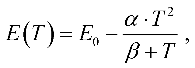
In the following we will discuss, how additional information from the PL spectra may be used to distinguish between the two possible cases, i.e. high negative (compressive) strain and low doping, or low positive (tensile) strain and high doping. The PL's maxima directly reflect the material's band structure. The detected photon energy is thus given by the energy related to the recombination of the induced electron hole pairs minus their binding energy.33 According to the DFT calculations strain induces delicate changes in the bandstructure which should be observable in the PL spectra. Because thermal processes usually obscure the intrinsic mechanisms of the excitonic transitions, low temperature measurements are of key importance for this task. Therefore, we took PL spectra of our Janus-type MoSSe monolayer at varying temperatures from RT down to T = 77 K. The results are plotted in Fig. 4(a). This graph shows an A- and a B-exciton at 1.755 eV and 1.921 eV, respectively, as well as a general red shift of these peaks with higher temperatures.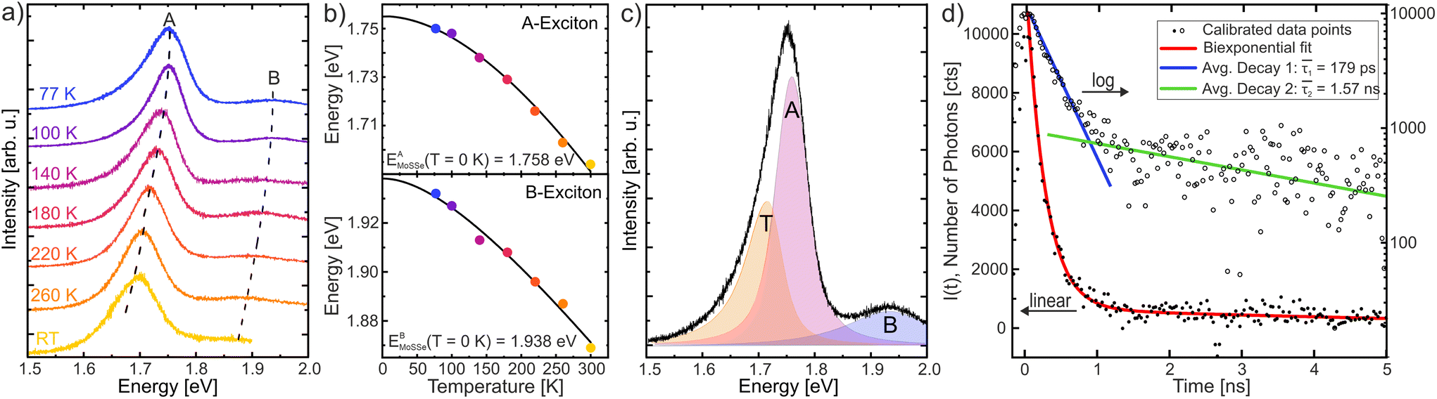 | ||
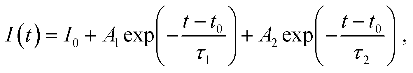
| Fig. 4 Evaluation of the temperature dependent exciton behaviour in MoSSe. (a) Temperature dependent, normalized photoluminescence spectra of Janus monolayer MoSSe indicating the red shift of the A and B exciton energies with higher temperatures. Visualized in (b) with Varshni fits for the two excitonic transitions. These indicate 0 K transition energies of 1.758 eV and 1.938 eV for A- and B-exciton, respectively. (c) Shows the 77 K PL spectra with the A- and B-exciton's, as well as the trion's (T) fit components. (d) Time-correlated single-photon counting measurement of Janus monolayer MoSSe plotted with a linear (left) and logarithmic (right) scale ordinate. The linear plot shows the bi-exponential fit (red) of the data, while the logarithmic data shows the two separate fit curves. Two decay processes can be deducted, a fast decay (blue) in the range of several hundred picoseconds and a slower decay (green) in the order of a few nanoseconds. | ||
The shift of the excitonic peak maxima can be plotted and fitted in excellent agreement with the Varshni relation34 as seen in Fig. 4(b). The Varshni equation is given as
 | (1) |
Fitting our data with this equation gives us additional, material specific information on our MoSSe monolayer, as well as its excitonic properties. Extrapolating our temperature dependent measurements to 0 K, we find transition energies of 1.76 eV and 1.94 eV for the A- and B-exciton, respectively. This is in good agreement with the theoretical value.31,35 Curiously, our values are larger than previously reported experimental results. A-exciton transition energies around 1.74 eV for both, 0 K extrapolated Varshni fits,17 and for 10 K measurements,19 are reported. A value our samples already exceed at 100 K. We believe that this is due to the fact that our base monolayer is exfoliated from a MoSe2 bulk crystal and as such is of better intrinsic quality than CVD samples used in the works cited above. As previously mentioned the strain on the flakes is increased for CVD samples, due to their stronger interaction with the substrate. The higher transition energies agree with this hypothesis, as a reduced E0 can be correlated to a higher density of defect states in the band gap in general22 and in Janus MoSSe,31 specifically. The interpretation of our PL signals as coming from band-edge excitons (rather than from excitons bound at defects) is further supported by the observation that first-principles calculations tend to predict even larger exciton transition energies than our experimental results for perfect Janus MoSSe monolayers under ideal conditions.7,13 As for the material specific coefficients, we report values of α = 3.78 × 10⁻⁴ eV K−1, and β = 214.06 K, or α = 3.94 × 10⁻⁴ eV K−1, and β = 230.05 K, as taken from the A- and B-exciton Varshni fits, respectively. The values for α and β align well with each other for both excitons. Furthermore, the Debye temperatures of standard TMDCs,36,37 as well as previous experimental data for MoSSe,17 are in good agreement with our data. For a comparison of the temperature dependent behaviour of the base TMDCs MoS2 and MoSe2 with the Janus monolayer, see ESI Fig. S3.†
While the PL's general temperature dependence speaks for a good quality Janus monolayer, we also find a low energy tail of the A-exciton peak in MoSSe, which gets more pronounced with lower temperatures. This is best visualized at 77 K in Fig. 4(c), where the A-exciton peak appears the most asymmetric. For monolayer MoS2, this asymmetric tail appears due to trion formation.38 This seems the most likely case here as well, due to the fact that it appears to have both, the same typical asymmetric distribution, as well as the same correlation with temperature as the trion tail in MoS2, where lower temperatures yield a stronger, and more distinct trion signature.38 Thus in (c) the components of the PL shown include a double peak in what we thus far denoted the A-exciton which in actuality describe both the A-exciton and the trion (T). Concluding from this strong trion formation, the Janus monolayer MoSSe must have excess charge carriers. The intrinsic charge carrier concentration nc can be approximated by comparing the A-exciton intensity IA with the charged trion's intensity IT. According to the mass action model39,40 a proportionality between the PL intensities and the charge carrier concentration can be given as
 | (2) |
Finally, we study the exciton dynamics in our Janus material as they can potentially show further effects of the strain and doping in the monolayer. The recombination processes of excitons and exciton complexes do not happen instantaneously, but on a time scale of a few hundred picoseconds after the excitation with the laser. We measured the lifetime of these processes by time-correlated single-photon counting (TCSPC, for details see method section). A representative calibrated TCSPC measurement at room temperature of monolayer MoSSe is shown in Fig. 4(d). The calibration spectrum is shown in the ESI Fig. S5.† Here, the data is plotted twice: once with a linear ordinate (left) corresponding to the solid dots, and once on a logarithmic scale (right) corresponding to the circles. The linearly plotted data shows best that the bi-exponential fits the data well. The general form of the bi-exponential function used to fit the data is given by
 | (3) |
 | (4) |
In the logarithmic data plot, it becomes more obvious that there are indeed two decay processes at work with different lifetimes. The blue line indicates the short-lived state. Its decay happens on a time scale of ∼200 ps. While the green line shows a longer lasting decay process on the order of several nanoseconds. This general behaviour of two decay processes with a slower and a faster component is in good agreement with measurements for MoS2 monolayers and other TMDCs.44,45 The true nature of the processes leading to the long and short lifetimes is still debated, however it seems clear that the long lifetime is due to a thermally driven process.37,46 At this point it is impossible to separate our data further into A-, B-exciton, and a trion lifetime; the lifetimes we report here are an amalgam of all of those processes including non-radiative recombination and dark excitons.
We measured the lifetime on several different spots on the monolayer to form an average. For the corresponding TCSPC measurements see Fig. S6 and for the fit parameter Table S3 in the ESI.† From this data, we report average lifetimes of ![[small tau, Greek, macron]](https://www.rsc.org/images/entities/i_char_e0d4.gif) 1 = 179 ps ± 48 ps for the fast decay, and 2 = 2.25 ns ± 1.46 ns for the slower decay, and an average total lifetime of tot = 1.57 ns ± 1.06 ns. Our fast decay lifetime corresponds nicely to previous time-resolved differential reflectance measurements of MoSSe by Zheng et al., where they concluded the exciton decay to occur on a time scale of 134 ps.32 These values are in good agreement with those reported for other TMDCs,44,45 however, it appears that they are slightly larger than those reported on average for unmodified MoS2. This could be due to the quantum-confined Stark effect arising from the intrinsic electric field in the Janus monolayer,47 which leads to less overlap of the electron and hole wave-functions, so that recombination occurs on a longer timescale.
1 = 179 ps ± 48 ps for the fast decay, and 2 = 2.25 ns ± 1.46 ns for the slower decay, and an average total lifetime of tot = 1.57 ns ± 1.06 ns. Our fast decay lifetime corresponds nicely to previous time-resolved differential reflectance measurements of MoSSe by Zheng et al., where they concluded the exciton decay to occur on a time scale of 134 ps.32 These values are in good agreement with those reported for other TMDCs,44,45 however, it appears that they are slightly larger than those reported on average for unmodified MoS2. This could be due to the quantum-confined Stark effect arising from the intrinsic electric field in the Janus monolayer,47 which leads to less overlap of the electron and hole wave-functions, so that recombination occurs on a longer timescale.
3. Conclusions
In summary, we have presented a method to produce Janus-type monolayers from exfoliating high-quality bulk materials and thermally sulfurizing them. We identified the Raman-shifts as a good indicator for strain and doping of the Janus monolayer by putting the shifts into the context of our DFT calculations. From this we could conclude that two possible combinations of strain and doping could be present in our samples: either a −0.8% compressed flake with n-type doping similar to MoS2 of −0.57 × 1013 cm−2 or a +0.4% stretched flake with a larger n-type doping of −1.18 × 1013 cm−2. With respect to strain we find both values viable. On the one hand, a small tensile strain is typically expected for exfoliated flakes, on the other hand, given the heating and cooling steps during the sulfurization, compressive strain is also feasible. However, when taking our data of the exciton behaviour into account, we find that the MoSSe exhibits a more pronounced trion formation than MoS2. As this can be directly linked to a larger n-type doping, we take this as evidence that the second option is more likely. Lastly, we report a total lifetime of excitons in MoSSe of 1.57 ns. The decay consists of a two-step process, yet we find evidence that the exciton decayoccurs on a time scale of 179 ps. These values are comparable with typical TMDCs, rendering the Janus material equally interesting for applications.4. Methods
4.1. Mechanical exfoliation
Our sample fabrication starts with monolayers mechanically exfoliated from bulk MoSe2. These are prepared onto a silicon substrate with a 285 nm oxide layer after two rounds of cleaning in an ultrasonic bath of laboratory grade acetone and ethanol. We use Nitto's Dicing Tape to thin down the bulk MoSe2 before pressing it onto the substrate with a heavy steel weight for approximately 30 minutes.4.2. Sulfurization process
In each run two exfoliated samples are put inside a multi zone tube furnace (ThermConcept ROK 70/750/12-3z) approx. 25 cm downstream of a solid sulfur source (85 mg, Sigma-Aldrich, 99.98% sulfur powder). Pure argon gas (99.9% Ar) is used as an inert carrier gas to purge the chamber before (15 min, 200 sccm) and during (75 sccm) the thermal processing. The exfoliated flakes are heated up to 800 °C. The sulfur is heated with a delay of 9 min up to 150 °C. Both temperatures are held constant for a process time of 20 min. At the end of the process the oven is opened to shock cool the chamber down to room temperature.4.3. Raman and photoluminescence spectroscopy
A WITec alpha300 RA confocal Raman spectrometer was used for both Raman and PL measurements. All measurements were done with a green laser (λ = 532 nm) with an output power of 0.5 mW. Grid sizes were switched between 600 l mm−1 for PL and mappings and the 1800 l mm−1 grid for single spectra measurements. The low temperature PL measurements were made possible by installing a Linkam Stage THMS350EV extension temperature control system to our Raman spectrometer.4.4. Density functional calculations
To explore the strain and doping dependence of the Raman-active modes of a free-standing MoSSe layer, we used a periodically repeated unit cell with one formula unit MoSSe and a unit cell height of 30 Å normal to the 2D layer. First-principles calculations were carried out within the density functional theory (DFT) framework using the VASP code,48,49 version 5.3.3, with a plane wave cut-off energy of 500 eV. The ion–electron interaction was treated by means of the projector augmented wave method.50 The generalized gradient approximation of Perdew, Burke, and Ernzerhof (PBE)51 was used for the exchange–correlation functional. To take the van der Waals interactions into account, a correction to the conventional Kohn–Sham DFT energy and forces was applied in the form of the dDsC dispersion correction proposed by Becke and Johnson,52 similar to previous work on vibrational modes in MoS2.53 The electronic band structure was sampled on a 9 × 9 k-point grid in the 2D Brillouin zone. Electron doping was simulated by including a small amount of additional charge when calculating band occupations, such that the conduction band minima became occupied. Isotropic strain was simulated by scaling the lattice constant. For each lattice constant and doping, the atomic positions were re-optimized to reduce the norm of all forces below 0.001 meV Å−1. Subsequently, the vibrational frequencies were calculated at the Γ point (phonon wave vector q = 0) using density-functional perturbation theory and the in-built functionality of the VASP code, exploiting the crystal symmetry and including the ionic contribution to the dielectric polarization.4.5. Time-correlated single-photon counting
TCSPC Measurements were done at the same WITec alpha300 RA confocal Raman spectrometer, by using a PicoQuant LDH-D-C-405 pulsed laser with a wavelength of 405 nm and a pulse width of <50 ps. For the single-photon detection an avalanche photodiode (resolution: <50 ps, range: 400–1050 nm, dark count rate: <50 cts per s) and a time to digital module were used. Calibration of the measurement was done without the laser irradiation, beforehand. For a representative calibration spectrum see the ESI Fig. S5.† Measurements were done at RT with a repetition frequency of 40 MHz, over a 25 s integration time on a time scale from 0 to 25 ns (1024 time bins), yielding a resolution of 30 ps per time bin. Each final spectrum (as the one shown in Fig. 4(d)) was then averaged over 30 single measurement.Author contributions
J. S. and M. S. are responsible for the conceptualization of the project and experiments. J. S. analyzed and evaluated the data, J. S. and V. M. performed the TCSPC-, LT-PL- and Raman measurements. E. P. contributed to the TCSPC measurements and evaluation of the data. St. S. and A. M. contributed to the LT-PL measurements and their interpretation. P. K. performed the DFT calculations. All authors discussed and contributed to the preparation of the manuscript.Conflicts of interest
There are no conflicts to declare.Acknowledgements
We thank the faculty of Physics of the University of Duisburg-Essen for a seeding grant and acknowledge the financial support from the Deutsche Forschungsgemeinschaft (DFG, German Research Foundation). This work is funded by the DFG through projects No. 501495566, 406129719, and 429784087 and through funding the project C05 of the Collaborative Research Center SFB1242 “Non-Equilibrium Dynamics of Condensed Matter in the Time Domain” (project No. 278162697).References
- A.-Y. Lu, H. Zhu, J. Xiao, C.-P. Chuu, Y. Han, M.-H. Chiu, C.-C. Cheng, C.-W. Yang, K.-H. Wei, Y. Yang, Y. Wang, D. Sokaras, D. Nordlund, P. Yang, D. A. Muller, M.-Y. Chou, X. Zhang and L.-J. Li, Nat. Nanotechnol., 2017, 12, 744–749 CrossRef CAS PubMed.
- J. Zhang, S. Jia, I. Kholmanov, L. Dong, D. Er, W. Chen, H. Guo, Z. Jin, V. B. Shenoy, L. Shi and J. Lou, ACS Nano, 2017, 11, 8192–8198 CrossRef CAS PubMed.
- R. Sant, M. Gay, A. Marty, S. Lisi, R. Harrabi, C. Vergnaud, M. T. Dau, X. Weng, J. Coraux, N. Gauthier, O. Renault, G. Renaud and M. Jamet, npj 2D Mater. Appl., 2020, 4, 1–8 CrossRef.
- R. Li, Y. Cheng and W. Huang, Small, 2018, 14, 1802091 CrossRef PubMed.
- L. Zhang, Z. Yang, T. Gong, R. Pan, H. Wang, Z. Guo, H. Zhang and X. Fu, J. Mater. Chem. A, 2020, 8, 8813–8830 RSC.
- Y. Wei, X. Tang, J. Shang, L. Ju and L. Kou, Int. J. Smart Nano Mater., 2020, 11, 247–264 CrossRef.
- A. C. Riis-Jensen, T. Deilmann, T. Olsen and K. S. Thygesen, ACS Nano, 2019, 13, 13354–13364 CrossRef CAS PubMed.
- L. Dong, J. Lou and V. B. Shenoy, ACS Nano, 2017, 11, 8242–8248 CrossRef CAS PubMed.
- R. Ahammed, N. Jena, A. Rawat, M. K. Mohanta, S. Dimple and A. de Sarkar, J. Phys. Chem. C, 2020, 124, 21250–21260 CrossRef CAS.
- A. Rawat, M. K. Mohanta, N. Jena, S. Dimple, R. Ahammed and A. de Sarkar, J. Phys. Chem. C, 2020, 124, 10385–10397 CrossRef CAS.
- Y. Ji, M. Yang, H. Lin, T. Hou, L. Wang, Y. Li and S.-T. Lee, J. Phys. Chem. C, 2018, 122, 3123–3129 CrossRef CAS.
- H. U. Din, M. Idrees, A. Albar, M. Shafiq, I. Ahmad, C. V. Nguyen and B. Amin, Phys. Rev. B, 2019, 100, 165425 CrossRef CAS.
- M. Idrees, H. U. Din, R. Ali, G. Rehman, T. Hussain, C. V. Nguyen, I. Ahmad and B. Amin, Phys. Chem. Chem. Phys., 2019, 21, 18612–18621 RSC.
- Y. C. Cheng, Z. Y. Zhu, M. Tahir and U. Schwingenschlögl, EPL, 2013, 102, 57001 CrossRef.
- M. Yagmurcukardes, Y. Qin, S. Ozen, M. Sayyad, F. M. Peeters, S. Tongay and H. Sahin, Appl. Phys. Rev., 2020, 7, 011311 CAS.
- H. Li, Y. Qin, B. Ko, D. B. Trivedi, D. Hajra, M. Y. Sayyad, L. Liu, S.-H. Shim, H. Zhuang and S. Tongay, Adv. Mater., 2020, 32, 2002401 CrossRef CAS PubMed.
- D. B. Trivedi, G. Turgut, Y. Qin, M. Y. Sayyad, D. Hajra, M. Howell, L. Liu, S. Yang, N. H. Patoary, H. Li, M. M. Petrić, M. Meyer, M. Kremser, M. Barbone, G. Soavi, A. V. Stier, K. Müller, S. Yang, I. S. Esqueda, H. Zhuang, J. J. Finley and S. Tongay, Adv. Mater., 2020, 32, 2006320 CrossRef CAS PubMed.
- K. Zhang, Y. Guo, Q. Ji, A.-Y. Lu, C. Su, H. Wang, A. A. Puretzky, D. B. Geohegan, X. Qian, S. Fang, E. Kaxiras, J. Kong and S. Huang, J. Am. Chem. Soc., 2020, 142, 17499–17507 CrossRef CAS PubMed.
- M. M. Petrić, M. Kremser, M. Barbone, Y. Qin, Y. Sayyad, Y. Shen, S. Tongay, J. J. Finley, A. R. Botello-Méndez and K. Müller, Phys. Rev. B, 2021, 103, 035414 CrossRef.
- Y.-C. Lin, C. Liu, Y. Yu, E. Zarkadoula, M. Yoon, A. A. Puretzky, L. Liang, X. Kong, Y. Gu, A. Strasser, H. M. Meyer, M. Lorenz, M. F. Chisholm, I. N. Ivanov, C. M. Rouleau, G. Duscher, K. Xiao and D. B. Geohegan, ACS Nano, 2020, 14, 3896–3906 CrossRef CAS PubMed.
- Y. Qin, M. Sayyad, A. R.-P. Montblanch, M. S. G. Feuer, D. Dey, M. Blei, R. Sailus, D. M. Kara, Y. Shen, S. Yang, A. S. Botana, M. Atature and S. Tongay, Adv. Mater., 2021, 2106222 Search PubMed.
- J. Hong, Z. Hu, M. Probert, K. Li, D. Lv, X. Yang, L. Gu, N. Mao, Q. Feng, L. Xie, J. Zhang, D. Wu, Z. Zhang, C. Jin, W. Ji, X. Zhang, J. Yuan and Z. Zhang, Nat. Commun., 2015, 6, 6293 CrossRef CAS PubMed.
- M. O'Brien, N. McEvoy, D. Hanlon, T. Hallam, J. N. Coleman and G. S. Duesberg, Sci. Rep., 2016, 6, 19476 CrossRef PubMed.
- H. Mehdipour and P. Kratzer, Phys. Rev. B, 2023, 106, 235414 CrossRef.
- E. Pollmann, L. Madauß, V. Zeuner and M. Schleberger, Encyclopedia of interfacial chemistry: Surface science and electrochemistry, 2017, vol. 3, pp. 338–343 Search PubMed.
- E. Pollmann, L. Madauß, S. Schumacher, U. Kumar, F. Heuvel, C. vom Ende, S. Yilmaz, S. Güngörmüs and M. Schleberger, Nanotechnology, 2020, 31, 505604 CrossRef CAS PubMed.
- J. E. Lee, G. Ahn, J. Shim, Y. S. Lee and S. Ryu, Nat. Commun., 2012, 3, 1024 CrossRef PubMed.
- A. Michail, N. Delikoukos, J. Parthenios, C. Galiotis and K. Papagelis, Appl. Phys. Lett., 2016, 108, 173102 CrossRef.
- S. Chu, C. Park and G. Shen, Phys. Rev. B, 2016, 94, 020101(R) CrossRef.
- C. Xia, W. Xiong, J. Du, T. Wang, Y. Peng and J. Li, Phys. Rev. B, 2018, 98, 165424 CrossRef CAS.
- C. Long, Y. Dai and H. Jin, Phys. Rev. B, 2021, 104, 125306 CrossRef CAS.
- T. Zheng, Y.-C. Lin, Y. Yu, P. Valencia-Acuna, A. A. Puretzky, R. Torsi, C. Liu, I. N. Ivanov, G. Duscher, D. B. Geohegan, Z. Ni, K. Xiao and H. Zhao, Nano Lett., 2021, 21, 931–937 CrossRef CAS PubMed.
- S. Borghardt, J.-S. Tu, F. Winkler, J. Schubert, W. Zander, K. Leosson and B. E. Kardynał, Phys. Rev. Mater., 2017, 1, 054001 CrossRef.
- Y. P. Varshni, Physica, 1967, 34, 149–154 CrossRef CAS.
- S. Arra, R. Babar and M. Kabir, Phys. Rev. Mater., 2019, 3, 095402 CrossRef CAS.
- S. Helmrich, R. Schneider, A. W. Achtstein, A. Arora, B. Herzog, S. M. de Vasconcellos, M. Kolarczik, O. Schöps, R. Bratschitsch, U. Woggon and N. Owschimikow, 2D Mater., 2018, 5, 045007 CrossRef CAS.
- T. Korn, S. Heydrich, M. Hirmer, J. Schmutzler and C. Schüller, Appl. Phys. Lett., 2011, 99, 102109 CrossRef.
- J. W. Christopher, B. B. Goldberg and A. K. Swan, Sci. Rep., 2017, 7, 14062 CrossRef PubMed.
- S. Mouri, Y. Miyauchi and K. Matsuda, Nano Lett., 2013, 13, 5944–5948 CrossRef CAS PubMed.
- J. S. Ross, S. Wu, H. Yu, N. J. Ghimire, A. M. Jones, G. Aivazian, J. Yan, D. G. Mandrus, Di Xiao, W. Yao and X. Xu, Nat. Commun., 2013, 4, 1474 CrossRef PubMed.
- Y. Lin, X. Ling, L. Yu, S. Huang, A. L. Hsu, Y.-H. Lee, J. Kong, M. S. Dresselhaus and T. Palacios, Nano Lett., 2014, 14, 5569–5576 CrossRef CAS PubMed.
- D.-H. Kang, M.-S. Kim, J. Shim, J. Jeon, H.-Y. Park, W.-S. Jung, H.-Y. Yu, C.-H. Pang, S. Lee and J.-H. Park, Adv. Funct. Mater., 2015, 25, 4219–4227 CrossRef CAS.
- B. Chakraborty, A. Bera, D. V. S. Muthu, S. Bhowmick, U. V. Waghmare and A. K. Sood, Phys. Rev. B: Condens. Matter Mater. Phys., 2012, 85, 161403 CrossRef.
- T. Guo, S. Sampat, K. Zhang, J. A. Robinson, S. M. Rupich, Y. J. Chabal, Y. N. Gartstein and A. V. Malko, Sci. Rep., 2017, 7, 41967 CrossRef CAS PubMed.
- T. Wang, Y. Zhang, Y. Liu, J. Li, D. Liu, J. Luo and K. Ge, J. Phys. Chem. C, 2018, 122, 18651–18658 CrossRef CAS.
- C. Robert, D. Lagarde, F. Cadiz, G. Wang, B. Lassagne, T. Amand, A. Balocchi, P. Renucci, S. Tongay, B. Urbaszek and X. Marie, Phys. Rev. B, 2016, 93, 205423 CrossRef.
- K. P. Dou, H. H. Hu, X. Wang, X. Wang, H. Jin, G.-P. Zhang, X.-Q. Shi and L. Kou, J. Mater. Chem. C, 2020, 8, 11457–11467 RSC.
- G. Kresse and J. Furthmüller, Phys. Rev. B: Condens. Matter Mater. Phys., 1996, 54, 11169–11186 CrossRef CAS PubMed.
- G. Kresse and D. Joubert, Phys. Rev. B: Condens. Matter Mater. Phys., 1999, 59, 1758–1775 CrossRef CAS.
- P. Blöchl, Phys. Rev. B: Condens. Matter Mater. Phys., 1996, 50, 17953–17979 CrossRef PubMed.
- J. P. Perdew, K. Burke and M. Ernzerhof, Phys. Rev. Lett., 1996, 77, 3865–3868 CrossRef CAS PubMed.
- A. D. Becke and E. R. Johnson, J. Chem. Phys., 2007, 127, 154108 CrossRef PubMed.
- S. Sarkar and P. Kratzer, J. Phys. Chem. C, 2021, 125, 26645–26651 CrossRef CAS.
Footnote |
| † Electronic supplementary information (ESI) available: Supplementary to the data shown here, we present topography images from atomic force microscopy measurements correlated with Raman mappings of the sample to ensure its homogeneity and monolayer status. Moreover, Raman spectra of a multilayer MoSe2 part of a sample after the processing are shown. This gives additional information on how the process cuts and replaces the Se-bonds and shows an as-processed heterostructure of a monolayer MoSSe on top of few-layer MoSe2. Additional analysis of DFT data for the doping and strain levels of monolayer MoS2 is provided to compare to the doping level of the Janus monolayer. Moreover, we present a more detailed comparison of the temperature-dependent PL of MoSSe in comparison with MoSe2 and MoS2, both of which show realistic values for the parameters of the respective Varshni-fits, corroborating our data for the Janus MoSSe monolayer further. Lastly, we present a calibration spectrum for the TCSPC measurement and explain some of its pitfalls, as well as spectra of the other TCSPC measurements from different points on monolayer MoSSe. See DOI: https://doi.org/10.1039/d3nr01978k |
| This journal is © The Royal Society of Chemistry 2023 |