
 Open Access Article
 This Open Access Article is licensed under a
 Creative Commons Attribution 3.0 Unported Licence
Defect pairing in Fe-doped SnS van der Waals crystals: a photoemission and scanning tunneling microscopy study†
Damla
Yesilpinar
a,
Martin
Vondráček
a,
Patrik
Čermák
b,
Harry
Mönig
 e,
Jaromír
Kopeček
a,
Ondřej
Caha
d,
Karel
Carva
c,
Čestmír
Drašar
b and
Jan
Honolka
*a
e,
Jaromír
Kopeček
a,
Ondřej
Caha
d,
Karel
Carva
c,
Čestmír
Drašar
b and
Jan
Honolka
*a
aInstitute of Physics, AV ČR, Na Slovance 1999/2, 182 21 Praha 8, Czechia. E-mail: honolka@fzu.cz
bFaculty of Chemical Technology, University of Pardubice, Studentská 573, 532 10 Pardubice, Czechia
cDepartment of Condensed Matter Physics, Charles University, Ke Karlovu 5, 121 16 Prague, Czechia
dDepartment of Condensed Matter Physics, Masaryk University, Žerotínovo nám. 617/9, 601 77 Brno, Czechia
ePhysikalisches Institut, Wilhelm-Klemm Str. 10, 48149 Münster, DE, Germany
First published on 20th July 2023
Abstract
We investigate the effect of low concentrations of iron on the physical properties of SnS van der Waals crystals grown from the melt. By means of scanning tunneling microscopy (STM) and photoemission spectroscopy we study Fe-induced defects and observe an electron doping effect in the band structure of the native p-type SnS semiconductor. Atomically resolved and bias dependent STM data of characteristic defects are compared to ab initio density functional theory simulations of vacancy (VS and VSn), Fe substitutional (FeSn), and Fe interstitial (Feint) defects. While native SnS is dominated by acceptor-like VSn vacancies, our results show that Fe preferentially occupies donor-like interstitial Feint sites in close proximity to VSn defects along the high-symmetry c-axis of SnS. The formation of such well-defined coupled (VSn, Feint) defect pairs leads to local compensation of the acceptor-like character of VSn, which is in line with a reduction of p-type carrier concentrations observed in our Hall transport measurements.
1 Introduction
Tin monosulfide (SnS) is a layered van der Waals (vdW) crystal with an orthorhombic structure shown in Fig. 1(a). It is a native p-type semiconductor with a bandgap Eg = 1.08 eV and room-temperature moderate carrier concentrations ranging typically from 1015 to 1018 cm−3 (ref. 1) and mobilities of 5–500 cm2 V−1 s−1.2 Due to its high optical absorption coefficients and nontoxic chemical properties, SnS is an interesting material for photovoltaic and sensor applications.3 The quasi-2D van der Waals (vdW) nature of the crystal structure bears the potential to form well-defined p–n junctions at the interface to n-type materials. Hereby, other layered 2D materials such as n-type MoS2 are particularly promising.4 On the other hand, the 2D crystal nature of SnS has the potential to host metallic guest atoms, e.g. in the vdW gaps between two neighboring SnS layers. Knowledge on atomic diffusion processes, which are governed by the bonding of guest atoms to the SnS host structure and its intrinsic defects, could be used to develop better battery concepts, e.g. based on Li ions.5 In view of possible SnS-based p/n-type homojunctions, e.g. for efficient solar cells, several works address the implementation of guest atoms into the SnS structure with the aim to push the carrier into the n-doped regime (see ref. 6 and references therein). In addition, the implementation of magnetic guests atoms is a standard approach to introduce spin degrees of freedom into semiconductors. For Sn-chalcogenides, we are aware of two recent density functional theory (DFT) studies addressing the bonding of dilute 3d transition metal guest atoms to SnSe and SnS layers for potential spintronic and magneto-optic applications.7,8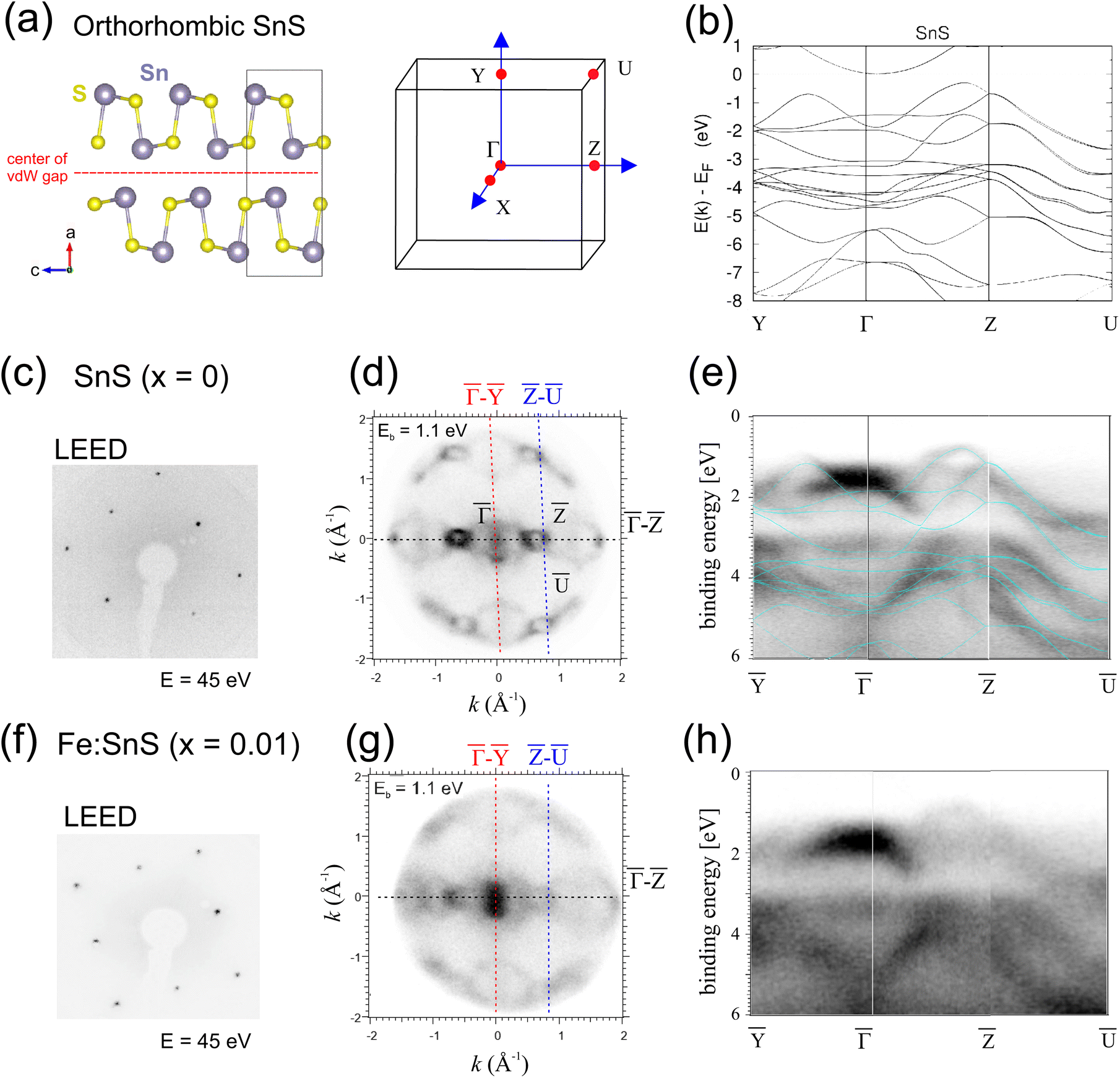 | ||
Fig. 1 (a) Side view of the layered orthorhombic SnS vdW structure (left) and a scheme of the respective Brillouin zone (right). We use the crystal space group Pnma. (b) DFT calculation of a defectless SnS band structure. (d and e) and (g and h): ARPES data of pure SnS (x = 0) and Fe![[thin space (1/6-em)]](https://www.rsc.org/images/entities/char_2009.gif) :SnS (x = 0.01) measured at T = 300 K and photon energies hv = 21.2 eV. (c) and (f) depicts LEED images after cleave. In (d) and (g) k-space intensities at a constant binding energy Eb = 1.1 eV are plotted. The dashed lines show high-symmetry k-space directions :SnS (x = 0.01) measured at T = 300 K and photon energies hv = 21.2 eV. (c) and (f) depicts LEED images after cleave. In (d) and (g) k-space intensities at a constant binding energy Eb = 1.1 eV are plotted. The dashed lines show high-symmetry k-space directions ![[capital Gamma, Greek, macron]](https://www.rsc.org/images/entities/char_e0ba.gif) – –![[Z with combining macron]](https://www.rsc.org/images/entities/char_005a_0304.gif) , –Ȳ, and –Ū, (e) and (h) present cuts through the photoemission intensity along the Ȳ–––Ū direction of the surface Brillouin zone. For x = 0 the DFT calculated band structure from (b) is overlaid. , –Ȳ, and –Ū, (e) and (h) present cuts through the photoemission intensity along the Ȳ–––Ū direction of the surface Brillouin zone. For x = 0 the DFT calculated band structure from (b) is overlaid. | ||
For all above mentioned applications, it is vital to gain a deep understanding of the stoichiometry-dependent formation of defect levels in SnS with and without guest atoms. While SnSe with its high thermoelectric figure of merit has been extensively studied by a wide range of methods, defects in SnS have been studied much less and mostly by theory. For native SnS, recent DFT works suggest that vacancy and antisite defects enthalpies depend on the Fermi level position EF with respect to the valence band maximum (VBM). Fermi levels close to the VBM ((EF − EVBM < 0.4 eV) sulfur vacancies VS2+ are predicted to have the lowest formation enthalpy, while at higher Fermi energies tin vacancies VSn2− and SnS− antisite defects become favorable.9,10 Due to the presence of both doubly-ionized VS2+ donor and single-ionized SnS− or VSn− acceptors, native SnS is expected to be an intrinsically compensated p-type semiconductor. For SnS materials grown under S-rich growth conditions, the compensation will involve only small concentrations of VS defects.10–13
The possibility to turn SnS into a n-type semiconductor by metal atom implementation was addressed by DFT for Sn or Bi atoms,14 which energetically seem to favor donor-type Sn-substitutional sites. Other DFT works taking Pb as guest atoms also suggest substitutional PbSn as a preferred defect but moreover propose a more complex scenario where the isoelectronic Pb substitution reduces the enthalpies for the generation of other interstitial Sn and/or Pb defects.10 For magnetic guest atoms, ab initio DFT calculations on single point defects predict that 3d transition metal atoms (TM: Mn, Fe, Co) should preferentially occupy Sn-substituting TMSn positions with acceptor-like character.7 However, it was also pointed out that Fe defects can lower their formation energies by structural relaxation in the vicinity of intrinsic vacancy defects such as VS, thereby forming a coupled defect pair.8 So far, there is, however, no experimental data to put such theory predictions to the test.
In this work we present a combined experimental and DFT study of atomic defect formation in melt-grown SnS crystals in their native states and in the presence of small magnetic Fe atom concentrations below 1 at%. Unlike expected for acceptor-like FeSn substitutional defects, we observe that p-type carriers in native SnS with carrier densities in the range of a few1017 cm−3 are significantly compensated when diluted Fe atoms of 0.7 at% are added. From atomically resolved STM imaging and density functional theory, we are able to assign this carrier compensation to the formation of electronically neutral acceptor/donor-like (VSn, Feint) defect pairs with a magnetic moment of 2.40μB. Within this coupled defect pair configuration, Feint corresponds to a heavily relaxed interstitial Fe atom position in the middle of the SnS layer slab and in close vicinity to the Sn-vacancy VSn. In ultraviolet photoemission spectroscopy, this local compensation of shallow acceptor VSn defects becomes visible as a shift of the valence band maximum to higher binding energies, consistent with an increasing influence of VS sulfur vacancy defects states deep in the gap.
2 Results
2.1 Characterization by photoemission spectroscopy
Bulk Sn(1−x)FexS samples (x = 0, x = 0.01), grown by free-melt cooling (FMC) techniques,15 were cleaved under UHV conditions by scotch tape exfoliation along the planes of the vdW gap depicted in Fig. 1(a). In the following, we will refer to the respective samples as SnS (x = 0) and Fe:SnS (x = 0.01). In this paper we use the crystal space group Pnma to describe the SnS structure. Sharp low-energy electron diffraction (LEED) patterns in Fig. 1(c) and (f) reflect a clean (100) surface crystal symmetry of the SnS reciprocal lattice structure shown on the right side in Fig. 1(a). A calculated band structure of defect-free SnS is shown in Fig. 1(b). DFT calculations are based on the full-potential linear augmented plane wave (FP-LAPW) method, as implemented in the band structure program ELK16 (see ESI† for details).
Angle-resolved photoemission spectroscopy (ARPES) was done at room temperature with the help of a Scienta-Omicron NanoESCA instrument and a non-monochromatized He lamp (hv = 21.2 eV). At x = 0 the (kx, ky)-space cut through the onset of valence band (VB) at binding energy Eb = 1.1 eV in Fig. 1(d) reveals the characteristic two-fold crystal symmetry and intense hollow square features close to , corresponding to hole-pockets as reported by ref. 17 for hole-doped SnS crystals. The overlay our DFT calculated band structure on energy-dispersive ARPES data in (e) reveals a rather good agreement along the fundamental directions Ȳ–––Ū. The VBM defined by the top of parabolic bands at appears 0.8 eV below the analyzer Fermi level (Eb = 0), according to a binding energy (BE) deep in the SnS band gap for SnS (x = 0). Cui et al. found the VBM position at about 0.65 eV for intrinsic p-type SnS.14 It is important to note that since the Fermi level in semiconductors generally varies with the degree of doping, the energy alignment of ARPES data with respect to the analyzer Fermi level can be subject to complex shifts, e.g. also due to band bending.
Fig. 1(g and h) shows respective ARPES data of Fe:SnS (x = 0.01) again prepared by in situ cleavage. The presence of Fe generally leads to a strong blurring in the SnS ARPES features and a larger diffuse background intensity, indicative of an increased disorder. No new band features appear. In the energy cut at Eb = 1.1 eV (Fig. 1(g)) features like the hollow squares at have considerably narrowed, suggesting a shift of the VBM to higher energies.
Energy shifts in the VB can be best quantified in the k-space integrated UPS mode. Fig. 2(a) shows the UPS intensity in the BE range [−1, +20] eV for x = 0 and x = 0.01. At low BEs the onset of the VBM intensity can be fitted linearly (leading edge method) as shown in Fig. 2(b). We define the position of the VBM as the intersection of the linear fit with zero intensity, which gives a VBM position approximately 0.7 eV below the analyzer Fermi edge in the case of pure SnS. The value suggests a Fermi level deep in the band gap, where according to DFT calculations charged tin vacancies VSn2− or SnS− antisite defects are located.9,10 We have confirmed this Fermi level position also at a higher photon energy of 1486.6 eV (Al Kα line), which gives a VBM position of (0.70 ± 0.05) eV. A similar value of 0.78 eV was previously reported for exfoliated few-layer thick SnS nanoflakes.3
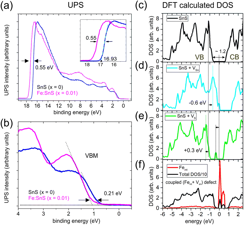 | ||
| Fig. 2 (a) Full scans of the ultraviolet photoemission intensity of SnS (x = 0) and Fe:SnS (x = 0.01) samples including the secondaries cut-off energies. The data was measured at T = 300 K with photon energies hv = 21.2 eV. (b) Shows the energy region corresponding to the VBM in detail. The leading edge approximation (dashed lines) suggests that the VBM is about 0.7 eV below the analyzer Fermi edge. Fe induces a rigid shift of the VB to higher BEs by +0.21 eV. (c) DFT calculations of the DOS of the host SnS structure (c) and with tin (VSn) (d) or sulfur (VS) (e) vacancy defects. (f) DOS for a coupled (VSn, Feint) defect pair (see also structural model in Fig. 5(f)). | ||
For x = 0.01 we observe a shift of the VBM by +0.21 eV to higher BEs in UPS, indicating less p-type properties. It suggests altered defects types and concentrations during growth with Fe. A similar shift of the VBM to higher BEs is also observed in UPS data of p-type SnS at increasing Sn concentrations, which lower the density of p-type Sn-vacancies.18 We exclude possible artificial shifts of UPS data towards higher BEs due to photoemission-induced charging of the sample, since carrier concentrations at room temperature are reasonably high (see Table 1 and further discussions in the XPS section).
:SnS (x = 0.01). The values were measured by Hall transport at T = 300 K. For comparison we also show reference data of a Bridgman-grown (B) SnS sample without iron contents
| Fe-content x | Carrier density (cm−3) | |
|---|---|---|
| SnS (FMC) | 0 | 3.0 × 10¹⁷ |
| Fe–SnS (FMC) | 0.01 | 0.5 × 10¹⁷ |
| SnS (B) | 0 | 3.5 × 10¹⁷ |
At high BEs the UPS intensity drops sharply due to the cut-off energy Ec of secondary electrons, which is known to be related to the work function φ via φ = hv − Ec. For x = 0 we derive a value Ec = 16.93 eV (see inset of Fig. 2(a)) corresponding to φ = 4.27 eV. DFT calculations predict similar values of φ = 4.32 eV for defect-free SnS.19 In the experimental literature slightly higher values in the range (4.45 ± 0.3) eV have been reported, e.g., in ref. 18. For iron concentrations x = 0.01, we see a substantial energy shift in the cut-off energy, indicating a reduction of the work function by 0.55 eV. For semiconducting 2D materials, we generally expect work functions to change e.g. due to variations in surface band bending and shifts in the Fermi level.20 It is known that the measured work function depends on the Fermi level position, and thus can vary for p-type or n-type doping of semiconductors.21 The electron affinity χ defined as the energy difference between the conduction band minimum (CBM) and the vacuum level (χ = Evac − ECBM) is much less dependent on the doping and is therefore a better material parameter to relate the work function to properties of a semiconductor. The work function is then given by φ = χ + Eg − (EF − EVBM), where Eg stands for the gap energy. Our observed trend of a work function reduction under the influence of Fe is qualitatively consistent with the measured shifted of the VBM by +0.21 eV to higher BEs. We comment that first theory predictions suggest rather small values χ = 3.52 eV.18
Fig. 2 shows a comparison of DFT-calculated density of states (DOS) for defectless SnS (c), as well as SnS with VSn (d), and VS defects (e). For comparison a coupled defect consisting of a VSn and an interstitial Fint is shown in (f), which will be discussed in detail in the next section. At absence of defects the DFT-derived band gap is about 1.2 eV (Fig. 2(c)), which slightly overestimates literature experimental values of 1.08 eV for SnS. Fig. 2(d) shows that VSn creates shallow donor states close to the VBM. Here, DFT predicts the Fermi level (E = 0) to be located in the acceptor states, which leads to a negative rigid shift of characteristic peaked VB features by −0.6 eV (see horizontal arrow in (d)). On the other hand, VS vacancies create defect states deep in the gap as calculated in Fig. 2(e), leading to a rigid shift of the DOS to higher BE by about +0.3 eV. The overall p-type carrier character of our samples in transport measurements (Table 1) is in line with the interpretation of a compensated p-type semiconductor with minor amounts of VS defects.10–13 The shift of the VBM by +0.21 eV under the influence of Fe (x = 0.01) can be explained by a compensation of p-type VSn defects, visible as a less p-type experimental carrier density shown in Table 1. Unlike in the substitutional FeSn case, Fe atoms in interstitial positions will act as donors and can shift the VBM to higher BEs. DFT calculations in Fig. 2(f) shows such a scenario for a coupled defect combination, which we will discuss in detail in the STM section.
Element specific changes in local coordination, e.g., due to defect formation, should become visible as chemically shifted components in tin and sulfur core level (CL) spectra in X-ray photoemission spectroscopy (XPS). Surface sensitive XPS measurements (probing depth ≈1 nm) on the in situ UHV cleaved SnS (x = 0) and Fe:SnS (x = 0.01) crystals are summarized in Fig. 3. The XPS wide scans in Fig. 3(a) are dominated by contributions from the elements Sn and S CLs. Very little C 1s intensity is visible from carbon contaminants, confirming clean surface properties after UHV cleavage. Highly resolved XPS data of Sn 4d, S 2p, and Fe 3p CLs are shown in Fig. 3(b)–(i).
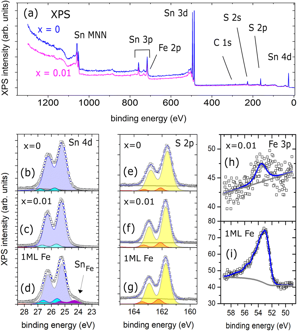 | ||
| Fig. 3 XPS data measured with monochromatized Al Kα light. (a) Shows wide scans of UHV-cleaved SnS (x = 0) and Fe:SnS (x = 0.01) crystals. (b), (c) and (e), (f) show respective Sn 4d and S 2p core levels data with high resolution. For comparison XPS spectra of SnS after 1 ML Fe deposition at room temperature are shown in (d) and (g). Fits are added to the data (details on the fit procedures are given in the ESI†). (h) and (i) compare Fe 3p core levels of SnS (x = 0.01) and the SnS surface after 1 ML Fe deposition. | ||
We start our discussion by looking at pure SnS (x = 0). Sn 4d and S 2p CLs generally exhibit narrow line shapes, which can be fitted by spin–orbit split Voigt doublets (see ESI†). The fitting procedure reveals that two doublets are needed in both cases as shown (b) and (e). For Sn2+ and S2− valences in defectless SnS we expect only two components, however, slightly asymmetric CL line shapes towards higher BEs are not unusual for in situ cleaved chalcogen-based vdW crystals, observed for example in Se 3d and Bi 5d CLs of clean Bi2Se3 surfaces.22 Asymmetries can be caused, e.g., by band bending effects at the surface, which leads to energy shifts in the same direction for Bi and Se CLs. We comment, that our observed second minor components in Sn and S CLs could also reflect a minority fraction of Sn and S atoms in an altered chemical state, e.g. in the close vicinity of vacancy defects. However, nearest neighbor vacancy defects should lead to opposite shifts in Sn and S CLs: fully ionized tin vacancies VSn will generate positive charge carriers, while a sulfur vacancy VS will generate two negative charge carriers (i.e., electrons). For example, in the case of bulk SnS2 crystals, a S-deficiency was reported to produce a significant chemical shift in the Sn 3d CLs by about 1.2 eV to lower BEs,23 reflecting the reduction of positive Sn charge in the presence of a neighboring donor-type S vacancy. We conclude, that in our case, element specific chemical shifts due to vacancy defects seem to be well below the detection limit of XPS, which fits to our low defect densities observed in STM (see discussion below) and a SnS stoichiometry close to 1:1.
A respective overview XPS spectrum of Fe-containing Fe:SnS (x = 0.01) is shown in Fig. 3(a). Looking at the resolved CLs of Sn and S in Fig. 3(c) and (f), no significant changes in the line shapes are observed compared to those measured for x = 0. It suggests that also here changes in the local tin and sulfur chemical state induced by the presence of low Fe concentrations are below our detection limit in XPS. However, for x = 0.01 we see that Sn 4d and S 2p CLs are shifted to slightly higher BEs by about +0.11 and +0.03 eV, respectively. The shifts are in the same direction as the above discussed rigid shift of the VBM by +0.21 eV (Fig. 2(b)), which we tentatively assign to a Fermi level shift towards defects deep in the gap.
From the Fe 3p CL intensity in Fig. 3(h) we can estimate the Fe concentration of the sample with x = 0.01: comparing the ratio between Fe 3p and Sn 4d intensities, and taking into account element specific photoabsorption cross-sections (see details in ESI†), we deduce an Fe concentration of (0.7 ± 0.2) at. % (Fe 2p CLs with a stronger intensity were not evaluated here, because of the overlap with Sn 3p CLs in the XPS spectrum). The Fe concentrations estimated from surface sensitive XPS can be compared to bulk sensitive energy-dispersive X-ray spectroscopy (EDX) measurements. Here, spatially resolved EDX shows a homogeneous diluted Fe background level of (0.15 ± 0.01) at%. We comment that in EBSD we also observed the formation of elongated, typically 10 × 100 micron sized hexagonal troilite FeS platelets (density 5–10 cluster per mm2) with a low areal coverage of <0.5%. The large FeS platelets can be easily recognised from their different stoichiometry in XPS and their entirely different, metallic, band structure detectable by photoemission with 40μm-scale lateral resolution. This work's photoemission data does not include contributions from such FeS platelets.
In order to understand more on Fe atom integration into SnS we study the adsorption behavior of Fe atoms on a pure SnS surface SnS (x = 0) as a reference system: about 1 monolayer (ML) of Fe was deposited onto a cleaved SnS crystal surface at room temperature under UHV conditions. Measuring XPS after deposition gives important insight into the Fe adatom bonding behavior at the Sn and S atom terminated SnS surface. The CLs shown in Fig. 3(d) and (g) reveal that upon Fe deposition only Sn develops a new Voigt-doublet component at about 24.2 eV. This new component corresponds to a more metallic state of Sn visible −0.9 eV shifted with respect to the dominating Sn2+ state (also for metallic SnAu alloys, a Sn 4d peak positions at 24.2 eV was reported24). Sulfur on the other hand shows no significant changes in the S 2p CL shape and thus remains in its original S2− state. From comparable layered vdW chalcogenide compounds like Bi2(Se, Te)3 it is known that 3d adatoms like Fe tend to strongly relax into the terminating chalcogenide atomic layer and hybridize with the respective anionic element in the 2nd atomic layer. Also there, Fe adatoms induce a metallic Bi CL component in Bi2(Se, Te)3 shifted by −0.72 eV with respect to the ionic Bi3+ state, while the respective chalcogen CL shapes remain less affected.25 In analogy, we do not expect diluted Fe atoms to reside in the center of the SnS vdW gaps (FevdW positions along the red line of Fig. 1(a)) – as we will further show in the next section – rather in heavily relaxed position with a certain proximity to Sn atoms.
It is moreover important to note, that the absence of significant shifts in the main S and Sn CL peak energy positions upon deposition of sizable amounts of Fe confirms that, despite the semiconducting properties of SnS, sample charging is not a relevant factor during our photoemission experiments.
2.2 STM characterization
The surfaces were imaged by a low temperature STM at T ∼78 K, revealing the atomic structure of the UHV cleaved SnS (x = 0) and Fe:SnS (x = 0.01) crystal surfaces (Fig. 4). The surface lattice periodicity for these samples were determined to be c: 4.4 ± 0.3 Å and b: 4.2 ± 0.2 Å, on pure, defect-free areas of the SnS surface. These values are in-line with the previously reported theoretical values for SnS,26 while bulk-sensitive neutron diffraction experiments reported smaller values c: 4.33 Å and b: 3.99 Å.27
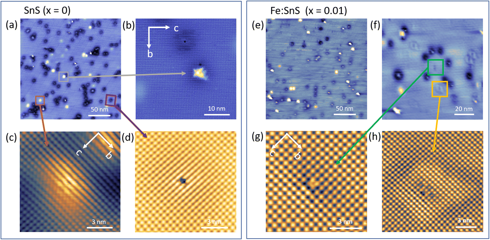 | ||
| Fig. 4 STM characterisation of in situ room-temperature cleaved SnS (x = 0) (a)–(d) and Fe:SnS (x = 0.01) (e)–(h) surfaces. STM images were taken at T = 78 K with a voltage Vbias = −1.20 V applied to the tip at a constant current Iset = 20 pA. (a) Shows an overview of the pure SnS sample. Three different intrinsic recurring contrast features (marked by boxes) were identified on this surface, which are imaged in (b–d) as close-ups. We identify (b) as a star-shaped defect, (c) a mound-like contrast, and (d) a movable feature surrounded by a dark halo. (e and f) present overview scans of the Fe:SnS (x = 0.01) surface at different scales, showing two additional recurring contrast features on this surface, imaged in (g and h) again as close-ups. The defects in (g) and (h) are named caterpillar and butterfly, due to the wing-like structures surrounding the defect. | ||
The overview STM images taken from the pure SnS surface, x = 0, in Fig. 4(a) revealed three recurring contrast features marked by squares. All three are shown in Fig. 4(b–d) in high resolution. The star-shaped features (denoted as star from hereon) show a strong resemblance to previously reported Sn vacancy (VSn) defects in SnSe28,29 and SnS30 crystals. In line with the literature, the orientation of the fourfold star is rotated by 45° with respect to the indicated crystal axes b and c in Fig. 4(b). As we will show further below, the 45°-rotated star geometry in STM contrast can be reproduced also by DFT assuming a surface VSn defect. VSn defects are thought to be the main defect responsible for the intrinsic p-type doping of pure SnS samples in line with our Hall transport results and our DFT calculations in Fig. 2(d). The statistics on the surface reveals that with a density (128 ± 48) μm−2, the star defect is the third most common defect found on the pure SnS surface. We have listed the STM-derived statistics of defect densities in Table 2 for comparison. It is important to note that while different cleaves of one and the same sample lead to variations in defect statistics on the surface, Table 2 reflects the overall trends.
:SnS (x = 0.01). All values are given in units [μm−2]
| star | mound | mobile | caterpillar | butterfly | |
|---|---|---|---|---|---|
| x = 0 | 128 ± 48 | 358 ± 130 | 1398 ± 432 | ||
| x = 0.01 | 260 ± 99 | 183 ± 21 | 955 ± 147 | 194 ± 75 | 55 ± 45 |
In Fig. 4(c), the second surface contrast feature is shown, which has a mound-like intensity enhancement (denoted as mound from hereon) with a lateral extension of few nanometers at Vbias = −1.20 V. The enhancement shrinks with increasing bias. As a consequence, at Vbias = −1.40 V the atomic structure is well resolved, revealing the absence of a surface point defect in its center (see ESI Fig. S1†). Such large scale contrast modulations without a surface atomic defect usually arise from imperfections located in the lower layers of the SnS vdW crystal, for example possible interstitial atoms11,12 or subsurface vacancies. The strong sensitivity of the modulation's lateral extension upon small bias voltage changes of the order 0.1 eV hint at the presence of tip-induced band bending effects, as observed, e.g., for subsurface defects in 2D semiconducting WSe2.31
Finally, we also observe mobile adsorbed species (denoted as mobile from hereon) on the surface indicated by the red box in Fig. 4(a). This third type of features are imaged as atomic-scale depressions surrounded by a circular nanometer-scale dark halo. The center atomic defect is scanned with high resolution in Fig. 4(d) taken at Vbias = −1.20 V. Under increased bias voltages (Vbias = −1.30 V and −1.40 V, I = 10 pA), these features are found to move as the tip scanned the selected area (ESI Fig. S2†), suggesting that these are adsorbed species on the surface and not atomic defects within the SnS crystal surface. The densities of the mound-like and the adsorbed features on the surface were found to be (358 ± 130) μm−2 and (1398 ± 432) μm−2, respectively. The fact that the density of mobile surface features are significantly higher than the mound-like subsurface defects suggests that they are not of the same origin. We believe that mobile species are molecules absorbed in UHV after cool-down of the in situ cleaved surfaces.
Fig. 4(e and f) present overview images taken on Fe:SnS (x = 0.01) surfaces, which again show the three abovementioned intrinsic contrast features (star, mound, and mobile), however, with altered densities. Furthermore, we identify two new contrast features occurring exclusively on Fe-containing SnS, which are marked in orange and green boxes. They are shown in Fig. 4(g) and (h) with higher resolution and are named caterpillar and butterfly, respectively. Like the mound defect, the latter shows a characteristic nanometer-scale intensity modulation around the defect, in this case with the shape of a distorted ring. Table 2 compares all defect statistics for x = 0 and x = 0.01, which are discussed in the following.
With respect to pure SnS, the densities of the recurring intrinsic contrast features at x = 0.01 were found as following: mobile defects with a density of (955 ± 147) μm−2 are comparable to that at x = 0 as expected, e.g. for adsorbed species. The density of mound contrast features have significantly decreased to (183 ± 21) μm−2. In contrast, star defects, which were identified as VSn, have increased to a density of (260 ± 99) μm−2. Lastly, the densities of the two newly identified contrasts, namely the caterpillar and the butterfly defects are found to be (194 ± 75) μm−2 and (55 ± 45) μm−2, respectively.
A correct identification of the two defects caterpillar and butterfly appearing exclusively on the Fe:SnS (x = 0.01) sample should reveal the mechanism how the Fe impurities are incorporated in the bulk of the SnS vdW crystals. The defects were therefore again imaged at different bias voltages to track the contrast evolution. In both cases, strong variations in contrast signatures are observed upon changes in Vbias of the order of 0.1 eV (ESI Fig. S3 and S4†). Like for the mound effect, we see that the nanometer scale ring modulation around the butterfly defect changes drastically and disappears at higher voltages Vbias = −1.30 V.
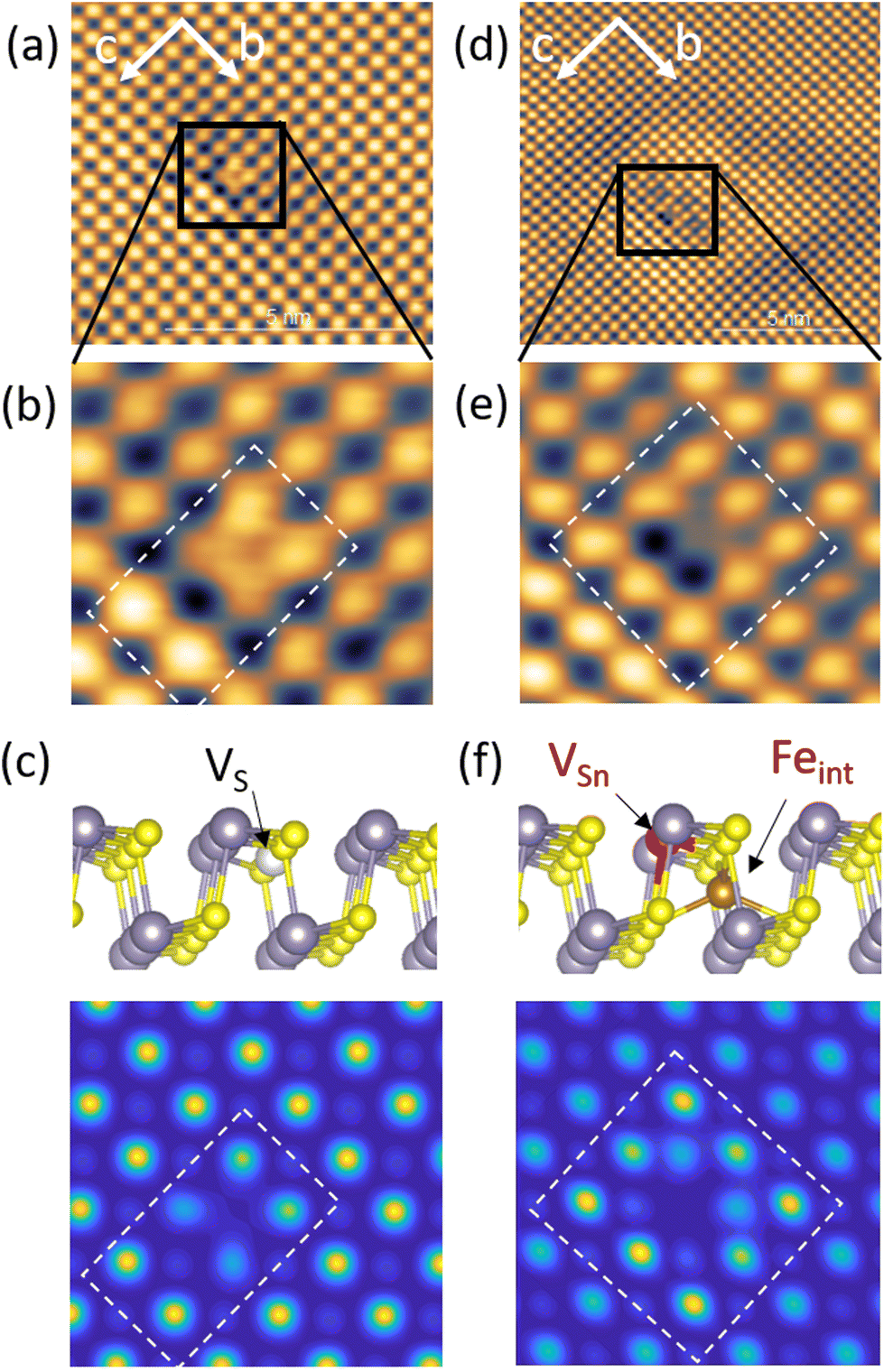
In order to interpret the observed point defects at the atomic scale, we then employed a Tersoff–Hamann approach in DFT, assuming different atomic defect types. Due to the need to describe a significant area surrounding the defect we have used a larger 5 × 5 × 1 supercell. Within the periodic supercell an 8.5 Å thick vacuum spacer was included to approximate the effect of the surface. STM images were then simulated using the Tersoff–Hamann approach,32 in which tunneling currents for the applied bias V are assumed to be proportional to the energy-resolved charge density n(r,E) integrated within the appropriate energy range:
 | (1) |
Here EF denotes the calculated Fermi energy and r(x,y,z) the position of the tip. In our STM configuration, negative experimental bias voltages Vbias correspond to respective positive V in eqn (1). In our calculations, z = 0 defines the scanning plane above the surface atom plane, which we assume to be at z = 0.12 (corresponds to about 1.37 Å) distance (see sketch in Fig. 6(a)). We have employed existing functions in the ELK code to obtain the charge density, but a custom modification was needed to evaluate it in an arbitrary specified energy range. The presence of a defect in a finite size supercell leads to a shift of the Fermi level, but the calculated STM figures are to be compared to the experimental situation where all defects are seen within one sample, thus with a constant Fermi level. Therefore for the evaluation of eqn (1) we shift the Fermi level so that the valence band top matches that of the ideal sample. Fig. 6 shows DFT calculations I(x,y,z = 0) for defectless SnS (b) and relevant single defect types VS, VSn, relaxed Feint, and FeSn [(c)–(f)].
 | ||
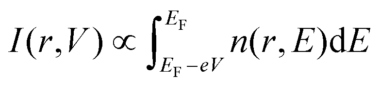
| Fig. 5 Determination of caterpillar and butterfly defects, observed exclusively on Fe:SnS (x = 0.01). (a) STM image of a caterpillar defect, which is shown in more detail in (b). (c) DFT calculations of a sulfur vacancy defect (VS) assuming a value V = 1.3 V in eqn (1). (d) STM image of a butterfly defect, shown in more detail in (e). (f) DFT calculations of a coupled (VSn, Feint) defect pair assuming a value V = 1.3 V in eqn (1). STM Images were taken at [Vbias = −1.20 V, Iset = 20 pA]. | ||
 | ||
| Fig. 6 STM contrast modelling from DFT calculations. (a) Shows a side-view of the defectless unit cell of SnS. S and Sn atoms are colored grey and yellow, respectively. A vertical scale z is added with it origin defined by the plane of the center of the top vdW gap (top red dashed line). The first atomic plane of Sn atoms is indicated at a vertical height z = 0.12 (dashed orange line) and the next vdW gap at z = 0.5 (lower red dashed line). In the calculations the tip apex is assumed to be at a constant height z = 0 (distance δz = 0.12 above the surface plane). (b) Calculated modulation I(x,y) for defectless SnS at tip apex height z = 0 using the Tersoff–Hamann with a value V = 1.3 V in eqn (1). (c)–(f) shows respective results for defects geometries VSn, VS, Feint, and FeSn shown in the left column. (x,y)-cuts at z > 0 (middle column) help to clarify the positions of the atomic defects, and cuts at z = 0 (right column) show the I(x,y) modulation, which models STM images. | ||
An area of about 7 × 7 nm2 including the caterpillar defect was scanned and the observed contrast at Vbias = −1.20 V (Fig. 5(a) and (b)) was compared with the DFT calculated modulations I(x,y,z = 0) reflecting the surface LDOS in the presence of different atomic defect types. It was found that the contrast signature that matched the most with the caterpillar feature was the S vacancy defect VS depicted in Fig. 5(c). Our assignment to VS is corrobated by previously reported STM data of Se vacancies in SnSe crystals which exhibit a almost identical STM contrast with a slight relaxation of the surrounding Sn atom pair along the c and b lattice directions.28 Scanning the VS defect at slightly higher bias voltages Vbias = −1.30 and −1.40 V we observed drastic changes in the contrast. At Vbias = −1.30 the atomic scale contrast of surrounding Sn atoms is inversed compared to Sn atoms far away from the defect. For Vbias = −1.40 the atomic contrast is finally lost in an extended clover-leaf shaped intensity, dominating the defect area (see ESI Fig. S3(b) and (c)†). Such drastic changes in contrast with respect to a small variations in the applied Vbias was previously reported, e.g., for Mn acceptor defects in semiconducting InAs crystals under the influence of tip-induced charging/decharging processes,33 creating ring-like features of several nanometer extension around the defect. Our observation of significant changes in nanometer scale modulations around the mound and butterfly defects strongly suggests the influence of the tip on the local Fermi level in our measurements. We believe that tip-induced charging/decharging process of the defect state due to local band bending is responsible for the obtained contrasts at different Vbias. We tried to estimate the influence of tip-induced band bending on the STM contrast from DFT for the case of VS defects. To this end, we calculated DFT images with the integrated energy range shifted to the positive side of the LDOS – mimicking local Fermi level shifts – as shown in ESI Fig. S3(e).† A change in atomic STM contrast from a depression in (d) to an enhancement at the VS defect is qualitatively reproduced and supports our interpretation.
The same procedure was utilized to determine the butterfly defect. The STM contrast observed on this defect at Vbias = −1.20 V is given in Fig. 5(d) and (e). A non-fourfold, arrow-like pattern is visible (marked by a dashed box in (e)), oriented antiparallel to the crystal c-axis and connected with a strong depression of intensity at the position expected for Sn. As discussed above, VSn defects alone appear as a quasi four-fold, 45°-rotated, star pattern, in line with our DFT calculated image in Fig. 5(d). The DFT contrast that matched best with the experimental butterfly pattern, is found to belong to a coupled defect geometry depicted in Fig. 5(f), composed of an acceptor-type VSn and a heavily relaxed donor-type interstitial Fe atom (Feint) at a close distance along the c-axis. A strong relaxation of Fe is conceivable due to the void from the neighbor Sn vacancy. The off-center Fe atom position used for the calculations corresponds to the one which maximises all nearest neighbor atom distances with an equal distance of 2.45 A. In the respective DFT-calculated image in Fig. 5(f) the STM-derived arrow-like contrast is reasonably well reproduced. From DFT this Feint position is energetically favorable compared to, e.g., the center positions in vdW gap (FevdW) by 0.37 Ryd per f.u. We find that the 2-fold symmetry of the coupled (VSn, Feint) defect is visible in STM at different bias voltages and respective calculations as shown in ESI Fig. S4.†
Our assignment of Fe-induced caterpillar and butterfly features to VS defects and coupled (VSn, Feint), respectively, implies that substitutional FeSn defects shown in Fig. 6(f) do not play a role in Fe-doped SnS under p-type conditions and Fermi energies deeper in the gap. At first glance this contradicts earlier DFT results in ref. 7, which claim that FeSn defects should be energetically favored. However, these works did not include coupled double-defect geometries. Instead, our findings support a recent DFT work by ref. 8 where the authors predict that Fe defects could also lower their formation energies by structural relaxation in the vicinity of intrinsic vacancy defects. Indeed, in the coupled (VSn, Feint) defect suggested in our work, Fe accommodates a site with a nearest neighbor distance of 2.45 Å, much smaller than in an unrelaxed substitutional FeSn cite with an Fe–S distance of 2.66 Å. The latter seems to be too large and therefore energetically not favorable. For comparison, e.g., in FeS2 with cubic pyrit structure the Fe–S distance is 2.29 Å.
Finally, we want to note that in the coupled defect state the interstitial Fe atom has a DFT calculated magnetic moment of 2.40μB. Thus, the (VSn, Feint) defect introduces a magnetic degree of freedom to the SnS systems, which could serve as a basis for spintronic concepts suggested in the literature.7,8 For that, an understanding of magnetic interactions between Fe atoms, e.g. mediated by delocalised carriers, would be of important, but respective studies by DFT were beyond the scope of this work.
3 Conclusions
We have thoroughly investigated ultra-high vacuum cleaved pure and Fe-doped SnS crystal surfaces (composition Sn(1−x)FexS with x = 0 and x = 0.01) by means of photoemission and scanning tunneling microscopy techniques with the aim to understand the formation of native and Fe-induced atomic defects in SnS. So far the implementation of magnetic atoms into SnS was only studied by theory, mostly using DFT methods.Hall transport measurements show that transport in our pure SnS samples is dominated by donor-type tin vacancy (VSn) defects leading to overall p-type carrier densities of the order of few 1018 cm−3. Photoemission spectroscopy using ultraviolet and X-ray light reveals Fe-induced shifts in the valence band maximum to higher binding energies, which is in line with DFT calculations assuming the compensation of VSn defects by Fe-induced donor type defects deep in the gap.
From atomically resolved STM data obtained from both, pure and Fe-doped SnS samples, it was possible to elucidate two mechanisms that lead to a decrease in the pristine p-type carriers in the SnS crystal. The first mechanism is the formation of donor-type VS defects in the Fe-doped samples. From STM statistics of pure SnS at absence of Fe, exclusively acceptor-like VSn vacancies are observed, which explains the known p-type character in SnS crystals. In the presence of Fe (x = 0.01), however, significant amounts of ambivalent VS midgap defects appear with densities of the order of 200 μm−2, similar to those of the low-energy acceptor VSn defects. A partial compensation of p-type defects is therefore expected and explains the reduction of the hole carrier density observed by Hall transport measurements.
As a second mechanism leading to compensation of VSn the integration of Fe is commonly proposed. Unlike predicted in earlier DFT works we do not observe substitutional FeSn defects, but interstitial donor-type Feint defects. From our STM studies, we conclude that interstitial Fe atoms do not appear as isolated defects but tend to couple to VSn defects along the high-symmetry c-axis of SnS. The close proximity to a Sn vacancy allows interstitial Fe to heavily relax towards the respective void.
Our results are important for possible SnS-based solar cell or sensor applications based on p–n junctions at the interface between 2D vdW materials. A detailed understanding on the atomic scale is necessary as the band alignment and carrier recombination dynamics depends on the type and distribution of defects in SnS. From our ultraviolet photoemission experiments we moreover report a significant decrease in the SnS work function by 0.55 eV under the influence of smallest amounts of Fe, which can be beneficial for performances of p–n devices.
Author contributions
DY, HM, MV, and JH realized with STM and photoemission experiments and respective data evaluations. CD and PC contributed with sample growth and Hall measurements. EBSD and EDX measurements were done by JK. KC and OC did the identification of defect geometries and respective DFT calculations.Conflicts of interest
There are no conflicts to declare.Acknowledgements
This work was supported by the Czech Science Foundation Grant No. 19-13659S. H. M. acknowledge support by the Deutsche Forschungsgemeinschaft DFG (Project MO 2345/4-1). We acknowledge CzechNanoLab Research Infrastructure supported by MEYS CR (LM2018110). The work is supported by Operational Program Research, Development and Education financed by European Structural and Investment Funds and the Czech Ministry of Education, Youth and Sports (Project No. SOLID21 – CZ.02.1.01/0.0/0.0/16–019/0000760). This work was supported by the Ministry of Education, Youth and Sports of the Czech Republic through the e-INFRA CZ (ID: 90254).References
- Yanuar, F. Guastavino, C. Llinares, K. Djessas and G. Masse, J. Mater. Sci. Lett., 2000, 19, 2135–2137 CrossRef CAS.
- L. A. Burton, D. Colombara, R. D. Abellon, F. C. Grozema, L. M. Peter, T. J. Savenije, G. Dennler and A. Walsh, Chem. Mater., 2013, 25, 4908–4916 CrossRef CAS.
- A. Jannat, F. Haque, K. Xu, C. Zhou, B. Y. Zhang, N. Syed, M. Mohiuddin, K. A. Messalea, X. Li, S. L. Gras, X. Wen, Z. Fei, E. Haque, S. Walia, T. Daeneke, A. Zavabeti and J. Z. Ou, ACS Appl. Mater. Interfaces, 2019, 42462–42468 CrossRef CAS PubMed.
- J. N. Olding, A. Henning, J. T. Dong, Q. Zhou, M. J. Moody, P. J. M. Smeets, P. Darancet, E. A. Weiss and L. J. Lauhon, ACS Appl. Mater. Interfaces, 2019, 11, 40543–40550 CrossRef CAS PubMed.
- M. Lin, D. Cheng, J. Liu, L. Ouyang, R. Hu, J. Liu, L. Yang and M. Zhu, Energy Environ. Mater., 2021, 4, 562–568 CrossRef CAS.
- I. Suzuki, S. Kawanishi, T. Omata and H. Yanagi, J. Phys.: Energy, 2022, 4, 042002 Search PubMed.
- C. Tang, Q. Li, C. Zhang, C. He, J. Li, T. Ouyang, H. Li and J. Zhong, J. Phys. D: Appl. Phys., 2018, 51, 245004 CrossRef.
- F. Wang, L. Zhou, Z. Ma, M. He, F. Wu and Y. Liu, Nanomaterials, 2018, 8(10), 789 CrossRef PubMed.
- Z. Xiao, F.-Y. Ran, M. Liao, H. Hiramatsu, K. Ide, H. Hosono and T. Kamiya, Phys. Chem. Chem. Phys., 2018, 20, 20952–20956 RSC.
- F.-Y. Ran, Z. Xiao, Y. Toda, H. Hiramatsu, H. Hosono and T. Kamiya, Sci. Rep., 2015, 5, 10428 CrossRef PubMed.
- J. Vidal, S. Lany, M. d'Avezac, A. Zunger, A. Zakutayev, J. Francis and J. Tate, Appl. Phys. Lett., 2012, 100, 032104 CrossRef.
- B. D. Malone, A. Gali and E. Kaxiras, Phys. Chem. Chem. Phys., 2014, 16, 26176–26183 RSC.
- Z. Xiao, F.-Y. Ran, H. Hosono and T. Kamiya, Appl. Phys. Lett., 2015, 106, 152103 CrossRef.
- J. Cui, C. Chen, W. He, J. Avila, L.-D. Zhao, M. C. Asensio, J. He and Y. Chen, J. Mater. Chem. A, 2018, 6, 24588–24594 RSC.
- K. C. Sraitrova, J. Cizek, V. Holy, J. Kasparova, T. Plechacek, V. Kucek, J. Navratil, A. Krejcova and C. Drasar, Phys. Rev. B, 2021, 103, 085203 CrossRef CAS.
- https://elk.sourceforge.net/ .
- W. He, D. Wang, J.-F. Dong, Y. Qiu, L. Fu, Y. Feng, Y. Hao, G. Wang, J. Wang, C. Liu, J.-F. Li, J. He and L.-D. Zhao, J. Mater. Chem. A, 2018, 6, 10048–10056 RSC.
- S. F. Wang, W. Wang, W. K. Fong, Y. Yu and C. Surya, Sci. Rep., 2017, 7, 39704 CrossRef CAS PubMed.
- M. P. Nasane, S. R. Rondiya, C. D. Jadhav, G. R. Rahane, R. W. Cross, S. Jathar, Y. Jadhav, S. Barma, D. Nilegave, V. Jadkar, A. Rokade, A. Funde, P. G. Chavan, R. L. Z. Hoye, N. Y. Dzade and S. Jadkar, New J. Chem., 2021, 45, 11768–11779 RSC.
- T. L. Quang, K. Nogajewski, M. Potemski, M. T. Dau, M. Jamet, P. Mallet and J.-Y. Veuillen, 2D Mater., 2018, 5, 035034 CrossRef.
- G. Shao, Energy Environ. Mater., 2021, 4, 273–276 CrossRef CAS.
- M. R. Scholz, J. Sánchez-Barriga, D. Marchenko, A. Varykhalov, A. Volykhov, L. V. Yashina and O. Rader, Phys. Rev. Lett., 2012, 108, 256810 CrossRef CAS PubMed.
- J. Zhang, D. Cao, Y. Wu, X. Cheng, W. Kang and J. Xu, Chem. Eng. J., 2020, 392, 123722 CrossRef CAS.
- P. Sadhukhan, S. Barman, T. Roy, V. K. Singh, S. Sarkar, A. Chakrabarti and S. R. Barman, Phys. Rev. B, 2019, 100, 235404 CrossRef CAS.
- M. Vondráček, L. Cornils, J. Minár, J. Warmuth, M. Michiardi, C. Piamonteze, L. Barreto, J. A. Miwa, M. Bianchi, P. Hofmann, L. Zhou, A. Kamlapure, A. A. Khajetoorians, R. Wiesendanger, J.-L. Mi, B.-B. Iversen, S. Mankovsky, S. Borek, H. Ebert, M. Schüler, T. Wehling, J. Wiebe and J. Honolka, Phys. Rev. B, 2016, 94, 161114 CrossRef.
- Y. Kumagai, L. A. Burton, A. Walsh and F. Oba, Phys. Rev. Appl., 2016, 6, 014009 CrossRef.
- T. Chattopadhyay, J. Pannetier and H. Von Schnering, J. Phys. Chem. Solids, 1986, 47, 879–885 CrossRef CAS.
- G. Duvjir, T. Min, T. T. Ly, T. Kim, A.-T. Duong, S. Cho, S. H. Rhim, J. Lee and J. Kim, Appl. Phys. Lett., 2017, 110, 262106 CrossRef.
- K. Asakawa, F. Oguro, Y. Yoshida, H. Sakai, N. Hanasaki and Y. Hasegawa, Jpn. J. Appl. Phys., 2019, 58, SIIA06 CrossRef CAS.
- X. F. Lu, Y. Zhang, N. Wang, S. Luo, K. Peng, L. Wang, H. Chen, W. Gao, X. H. Chen, Y. Bao, G. Liang and K. P. Loh, Nano Lett., 2021, 21, 8800–8807 CrossRef CAS PubMed.
- R. Zhang, G. Clark, X. Xu, P. T. Darancet and J. R. Guest, J. Phys. Chem. C, 2021, 125, 14056–14064 CrossRef CAS.
- J. Tersoff and D. R. Hamann, Phys. Rev. B, 1985, 31, 805–813 CrossRef CAS PubMed.
- F. Marczinowski, J. Wiebe, F. Meier, K. Hashimoto and R. Wiesendanger, Phys. Rev. B: Condens. Matter Mater. Phys., 2008, 77, 115318 CrossRef.
Footnote |
| † Electronic supplementary information (ESI) available. See DOI: https://doi.org/10.1039/d3nr01905e |
| This journal is © The Royal Society of Chemistry 2023 |