
 Open Access Article
 This Open Access Article is licensed under a Creative Commons Attribution-Non Commercial 3.0 Unported Licence
Built-in tensile strain dependence on the lateral size of monolayer MoS2 synthesized by liquid precursor chemical vapor deposition†
L.
Seravalli
 a,
F.
Esposito
ab,
M.
Bosi
a,
L.
Aversa
c,
G.
Trevisi
a,
R.
Verucchi
c,
L.
Lazzarini
a,
F.
Rossi
a and
F.
Fabbri
*d
a,
F.
Esposito
ab,
M.
Bosi
a,
L.
Aversa
c,
G.
Trevisi
a,
R.
Verucchi
c,
L.
Lazzarini
a,
F.
Rossi
a and
F.
Fabbri
*d
aInstitute of Materials for Electronics and Magnetism (IMEM-CNR), Parco Area delle Scienze 37/a, 43124 Parma, Italy
bDepartment of Mathematical, Physical and Computer Sciences, University of Parma, Parco Area delle Scienze 7/a, 43124 Parma, Italy
cInstitute of Materials for Electronics and Magnetism (IMEM-CNR), FBK Trento unit, Via alla Cascata 56/C, 38123 Povo, Trento, Italy
dNEST, Istituto Nanoscienze – CNR, Scuola Normale Superiore, Piazza San Silvestro 12, 56127 Pisa, Italy. E-mail: filippo.fabbri@nano.cnr.it
First published on 14th August 2023
Abstract
Strain engineering is an efficient tool to tune and tailor the electrical and optical properties of 2D materials. The built-in strain can be tuned during the synthesis process of a two-dimensional semiconductor, such as molybdenum disulfide, by employing different growth substrates with peculiar thermal properties. In this work, we demonstrate that the built-in strain of MoS2 monolayers, grown on a SiO2/Si substrate by liquid precursor chemical vapor deposition, is mainly dependent on the size of the monolayer. In fact, we identify a critical size equal to 20 μm, from which the built-in strain increases drastically. The built-in strain is the maximum for a 60 μm sized monolayer, leading to 1.2% tensile strain with a partial release of strain close to the monolayer triangular vertexes due to the formation of nanocracks. These findings also imply that the standard method for evaluation of the number of layers based on the Raman mode separation can become unreliable for highly strained monolayers with a lateral size above 20 μm.
Introduction
Strain engineering is an efficient tool to tune and tailor the electrical and optical properties of 2D materials since their electronic band structures are highly sensitive to mechanical deformation.1–8 Among the different classes of 2D materials, semiconducting transition metal dichalcogenides (TMDs) have demonstrated the most interesting and surprising modifications of electronic properties induced by the application of strain.9,10 For instance, strain can induce the indirect-to-direct bandgap transition in multilayer WSe2 flakes,11 while the opposite transition (the direct-to-indirect transition) can occur in monolayer TMDs.12,13 With regard to optical properties, local strain application can induce exciton funneling,14,15 efficient exciton to trion conversion16 or the formation of a new hybrid state of dark and localized excitons.17It is worth noting that TMD monolayers can withstand high tensile strains before breaking, as high as 10% for molybdenum based18,19 and 19% for tungsten based20 exfoliated monolayers.
Different approaches have been employed for the application of external stress to 2D materials: the most employed one is based on the use of bendable and stretchable polymeric substrates.21–28 where it is possible to apply mainly uniaxial strain to 2D materials. This approach is mostly used in the fabrication of origami-like29 and kirigami-like30,31 MoS2 based devices, such as strain sensors or optoelectronic devices. A similar approach has been employed to fabricate human eye mimicking photodetectors.32 Another widely used method is the transfer of a 2D material on a patterned non-planar substrate for inducing localized strain, resulting in a local change of the band structure. The substrate can present insulating33–36 or semiconducting37,38 structures, namely stressors, that can apply a large local strain degree at their top. This large localized strain application modifies the band structure of 2D semiconducting materials, enabling efficient charge collection, desirable for bright single photon emission.35,36 A high degree of strain is also achieved by suspending 2D membranes on hole patterned substrates.39 A local strain increase can be achieved on suspended membranes using different approaches: using an AFM tip,40 applying an external gas pressure41 or applying a gate voltage between a suspended monolayer membrane and an electrode below.17 An additional novel approach to apply strain to TMD heterostructures is the employment of polymeric artificial muscles, that taking advantage of the low friction between different 2D materials can apply a tensile strain in van der Waals heterostructures.42
The strain tuning during the chemical vapor deposition (CVD) process of 2D materials has also been demonstrated.43–45 This method relies on the mismatch of the thermal expansion coefficient (TEC) between the substrate and the 2D material.4 For instance, monolayer WSe2 with built-in strains ranging from 1% tensile to compressive 0.2% was obtained using different growth substrates. The TEC approach has also been employed in order to synthesize strained WS2 on quartz with an oriented array of wrinkles.46 In addition, strain induced buckling has been recently identified as a possible cause of threefold symmetric domain formation in hexagonal shaped WS2 monolayers.47 In the case of MoS2, the modification of strain and doping using different growth substrates has been demonstrated, where the maximum built-in tensile strain is found to be 0.4% with a SiO2 growth substrate.48
In this work, we demonstrate the dependence of the tensile strain as a function of the lateral size of sharp-vertex shaped MoS2 monolayers grown on a standard 300 nm thick SiO2/Si substrate by liquid precursor chemical vapor deposition. The built-in strain is demonstrated and evaluated by scanning Raman and photoluminescence spectroscopy. Monolayer MoS2, with a lateral size below 20 μm, presents a built-in compressive strain of 0.3%, while the flakes with the largest lateral size (60 μm) are more strained, reaching an upper limit of 1.2%. It is worth noting that such flakes are affected by nanocracks close to the vertexes, revealing a partial release of the strain down to 0.7%. The built-in strain affects the optical properties; in particular, the highly strained flakes show quenching and red-shifting of the excitonic emissions of MoS2.
Results and discussion
Fig. 1 illustrates the outcome of the CVD synthesis at increasing temperature using a solution containing a molybdenum liquid precursor. In particular, the sketch (Fig. 1a) shows the deposition of the precursor solution on the SiO2/Si growth substrate by spin coating, carried out for 30 s at 3000 rpm, of the precursor solution. This solution has three main components: a 3 mM solution of ammonium molybdate tetrahydrate (AMT), a 62.5 mM solution of sodium hydroxide (NaOH) and a 0.4 mM solution of iodixanol (Optiprep). Atomic force microscopy (AFM) was employed to study the number of layers composing the flakes and their lateral size. It is worth noting that the flakes obtained with the liquid precursor CVD have the sharp-vertex triangular shape.49 The lateral size data are reported in Fig. 1b, which highlights the increase of the flake size with the growth temperature. The flakes, grown at 810 °C, present an average lateral size of (15.1 ± 3.0) μm, while the flakes synthesized at 820 °C present an average lateral size of (24.1 ± 4.9) μm. The maximum lateral size, (58.2 ± 5.7) μm, is obtained when the growth process is carried out at 830 °C. Fig. 1c–e present the representative AFM topographical map of the flake obtained at increasing temperature. All the flakes, grown at the different temperatures, present fractal saw-toothed edges, which are probably mediated by a diffusion-limited-aggregation (DLA) regime.50,51 In addition, the flake edges present nanoparticle decoration. Such an effect is directly connected with the employment of the liquid precursor, since the nanoparticles are composed of precursor byproducts, such as sodium oxide (Na2O).52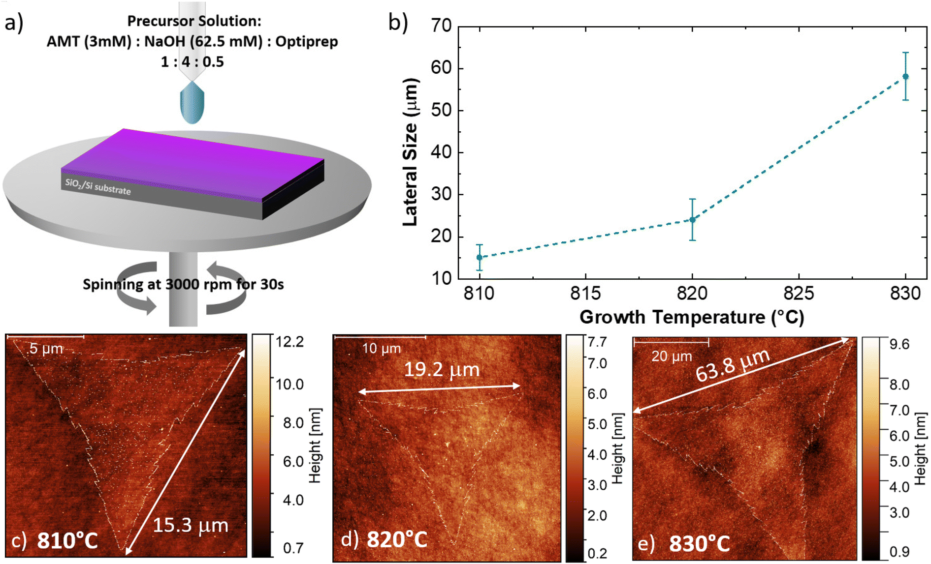 | ||
| Fig. 1 (a) Illustrative sketch of the substrate preparation prior to the growth process. (b) Dependence of the MoS2 monolayer lateral size versus the growth temperature of the CVD process. (c), (d) and (e) Representative AFM topographic maps of the MoS2 flake grown at different temperatures. The lateral size of the flake (white arrow) is 15.3 μm, 19.2 μm and 63.8 μm in the case of 810 °C, 820 °C and 830 °C growth temperatures, respectively. | ||
The AFM topographic maps, acquired on the edge of the flakes, are reported in Fig. 2. The main purpose of such analysis is the evaluation of the number of layers of the MoS2 flake and the morphological analysis of the nanoparticles (NPs) decorating the flake edges. The topographical analysis reveals the presence of nanoparticles of smaller size inside the MoS2 flake and on the SiO2 substrate. All the MoS2 flakes are monolayer: the height profiles reported on the different panels, reveal a flake thickness of 0.7–0.8 nm, the standard thickness of MoS2 monolayer.53–56 Cross-sectional TEM analysis is reported in Fig. S1,† confirming the monolayer nature of MoS2 obtained at 830 °C. It is worth noting that all the height profiles are acquired in the area of the flake not affected by the nanoparticles and the flakes synthesized at 810 °C and 820 °C present a few nanometer thick step on the edge, similarly to WS2 flakes grown by the CVD process using a tungsten liquid precursor.47 This effect is due to a strain induced delamination of the ML edges. The nanoparticles decorating the flake edges present a similar diameter, (26 ± 7) nm, while the height increases on increasing the growth temperature. In fact, the height of the nanoparticles varies from (8 ± 2) nm at 810 °C to (18 ± 5) nm at 830 °C, indicating that temperature has an important role in the formation of precursor byproducts. The density of the nanoparticles increases in the case of the growth carried out at 830 °C with an average linear density of nanoparticles of 32 NPs per μm, while the linear density decreases to 22 NPs per μm for the synthesis at lower temperatures. The statistical analysis of the NP morphology is reported in Fig. S2.†
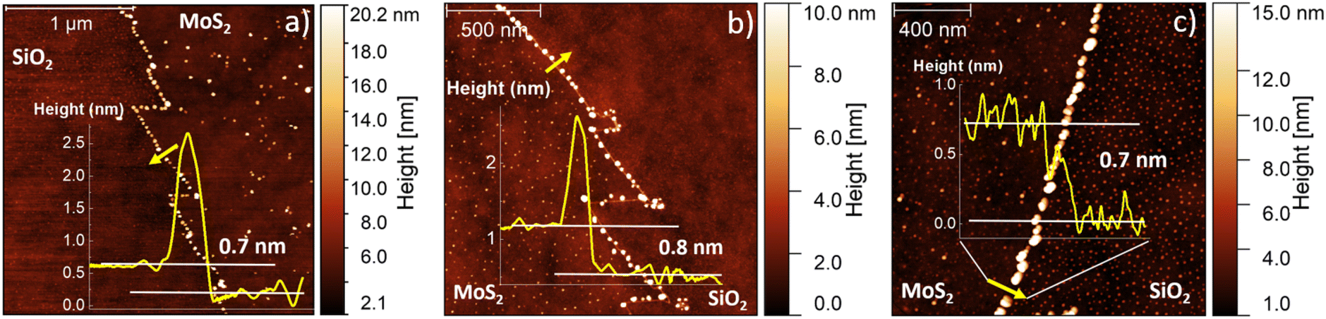 | ||
| Fig. 2 AFM topographic maps of the edges of the flakes grown at increasing temperatures (a) 810 °C, (b) 820 °C and (c) 830 °C. The height profiles are obtained where the yellow line is reported on each map. | ||
Fig. 3 presents the Raman characterization of the monolayer MoS2, synthesized at increasing temperatures. The representative Raman spectrum (Fig. 3a), acquired at the center of the flake grown at 810 °C (black line), presents the standard MoS2 Raman modes, E2g, at 383.6 cm−1 and A1g, at 403.5 cm−1, with a Raman mode separation of 19.9 cm−1. The A1g mode corresponds to the sulfur atoms oscillating in antiphase out-of-plane and the E2g mode is related to the sulfur and molybdenum atoms oscillating in antiphase parallel to the crystal plane.
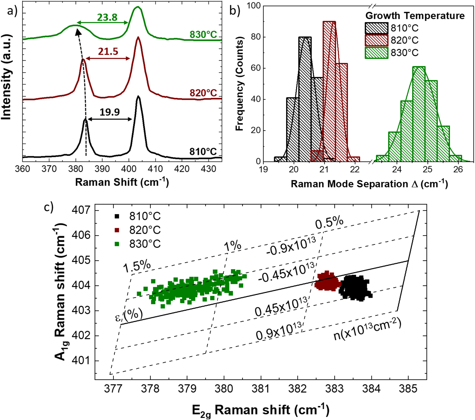 | ||
| Fig. 3 (a) Representative Raman spectra of the MoS2 monolayers obtained at increasing temperatures: 810 °C (black line), 820 °C (red line), and 830 °C (green line). The spectra are vertically shifted for the sake of clarity. The Raman mode separation is indicated for each spectrum. (b) Histogram of the Raman mode separation for the different growth temperatures. (c) MoS2 doping/strain correlation plot. | ||
The separation of the Raman modes below 20 cm−1 is the standard benchmark of monolayer MoS2.23,57,58 However, this analysis of the MoS2 monolayer grown at higher temperature demonstrates that both the MoS2 Raman modes are shifted. In fact, in case of the flake grown at 820 °C (red line) the E2g and the A1g modes appear at 382.5 cm−1 and at 404 cm−1, respectively. The separation of the Raman mode is 21.5 cm−1, a value standardly reported for bilayer MoS2.57,58 For the flakes grown at the 830 °C (green line) the A1g mode is still set at 404 cm−1, while the E2g presents an additional shift down to 380.2 cm−1. The separation of the Raman modes is 23.8 cm−1, the standard benchmark of few-layers MoS2.57,58 The larger shift of the E2g mode is a symptom of the presence of strain because the A1g mode is less affected than the E2g mode, being the A1g mode related to the out-of-plane vibration with respect to the E2g mode. In particular, the different response to strain of the two MoS2 Raman modes is reflected in the different Grüneisen parameter of each vibrational mode: γE2g = 0.68 and γA1g = 0.21.26,41,59 Another clue of the presence of built-in strain applied to the MoS2 grown at high temperature is the broadening of the E2g mode, whose full width at half maximum (FWHM) is from 2.5 cm−1 (810 °C grown monolayers) up to 10.4 cm−1 (830 °C grown monolayer);26 in fact, the application of strain induces the degeneracy breaking of the E Raman mode. The breaking of the degeneracy causes the splitting of the E2g mode in the case of the presence of uniaxial strain larger than 0.8%.21,27Fig. 3b reports the statistical analysis of the Raman mode separation, obtained by the Raman maps of a single flake shown in ESI Fig. S3.† The Gaussian distribution of the Raman mode separation is obtained by fitting the histogram data. In the case of the flakes synthesized at 810 °C, the distribution is centered at 20.4 cm−1 with a FWHM of 0.7 cm−1 and it becomes even sharper in the case of the synthesis at 820 °C with a FWHM of 0.5 cm−1, being centered at 21.3 cm−1. The largest distribution of the Raman mode separation is a FWHM of 1.4 cm−1 in the case of the 830 °C grown monolayers, where the Gaussian fitting reveals that the center is at 24.8 cm−1. The statistical analysis of the Raman mode separation is necessary to clarify the discrepancy with the AFM analysis reported in Fig. 2; in fact, all the flakes analyzed are monolayer in nature whereas the Raman results suggest a different number of layers for the increasing growth temperature. This is clear with regard to the different shifts of the two Raman modes when strain is applied to MoS2 because the E2g mode is more affected than the A1g mode, as previously explained. Therefore, we can assess that the presence of built-in strain in the MoS2 synthesis with liquid precursors makes the Raman method unreliable for the evaluation of layer number, using the separation of the vibrational modes. In order to quantify the built-in strain and the modification of doping, we employ the MoS2 correlation plot of the Raman shifts of the E2g and A1g modes, also known as the ε–n system.60 This method allows to disentangle and to quantify the strain and doping variations and it is normally employed for studying growth induced strain,61 the effect of different growth substrates48 or in MoS2 based van der Waals heterostructures.62,63 The full lines represent the zero strain and zero doping lines, while the dashed lines correspond to iso-strain and the iso-doping lines, calculated following the insights from previous works.41,64 In addition, it is worth mentioning the importance of the origin of the ε–n system: we set the zero strain and charge neutrality phonon frequencies 385 cm−1 for the E2g mode and 405 cm−1 for the A1g mode, evaluated in the case of CVD grown MoS2 suspended monolayer membrane.41 The data regarding the MoS2 monolayers grown at 810 °C present a round distribution revealing an average value of (0.29 ± 0.06)% of tensile strain and an average positive charge concentration of (0.23 ± 0.22) × 1013 cm−2, while in the case of the monolayer synthesized at 820 °C, the data distribution is less dispersed and the average tensile strain increases up to (0.44 ± 0.12)% and the charge concentration decreases close to neutrality, (0.06 ± 0.10) × 1013 cm−2. The average strain reaches its maximum in the case of the MoS2 monolayer obtained at 830 °C, (1.15 ± 0.5)%, albeit the data present a linear distribution along the iso-doping line relative to an electron charge concentration −0.45 × 1013 cm−2. In order to clarify the data spreading in the A1gversus E2g correlation plot, in the case of the monolayers obtained at 830 °C, the spatial distribution of strain is shown in Fig. 4. The methodology for the development of the strain maps is reported in Fig. S5† with the strain maps of the flakes grown at 810 °C and 820 °C. The Raman spectra in the amorphous carbon range are reported in Fig. S4† showing the absence of any amorphous carbon related peaks that can arise due to organic compounds (i.e. iodixanol) in the precursor solution. In addition, the data regarding the MoS2 MLs transferred on a clean SiO2/Si substrate are reported in Fig. S5.†
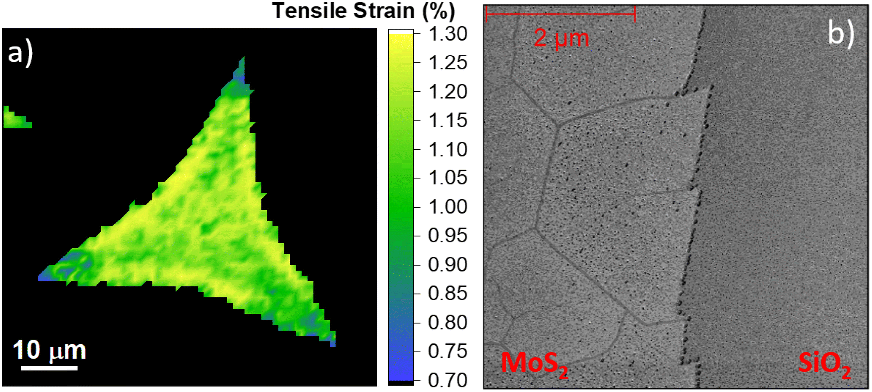 | ||
| Fig. 4 Representative strain map of the MoS2 monolayers obtained at 830 °C (panel a) and the AFM phase map of the edge of the flakes (panel b). | ||
The strain map of the 830 °C grown monolayer (Fig. 4a) reveals that the strain is partially released in the triangular vertexes of the flake. This finding supports the spreading of the data reported in Fig. 3c. In fact, while in the central part of the flake the strain is above 1%, it decreases to 0.7%–0.8% close to the vertexes of the triangular monolayer. The strain release mechanism is based on the formation of nanocracks in such regions, demonstrated by AFM phase analysis (Fig. 4b). The AFM phase analysis is employed to maximize the contrast of the nanocracks, and the topographical map is reported in Fig S6 of the ESI.† A similar strain release mechanism has been previously reported in the case of MoS2 monolayer exposed to hydrogen or oxygen plasma.65,66 The similarities rely mainly on the formation of a six-fold hexagonal patterned net of nanocracks. The angle distribution of the lines relative to the edge of the MoS2 crystal has preferential orientations of 0°, 60°, and 120° as shown in Fig. 4b, which indicates that the line patterns are associated with the crystallographic orientation of the MoS2. This effect is important because it demonstrates that the MoS2 monolayer can sustain a limited amount of built-in tensile strain during the growth process, while the strain applied by external procedures can reach 10%.18 The strain maps of the ML synthesized at 810 °C and 820 °C are reported in Fig. S7.†
Another method for evaluating the strain in atomically thin semiconducting TMDs is the analysis of the photoluminescence (PL) emission. Several previous works have demonstrated the strain dependence of the PL emission energy and intensity.21,22,27,41,44,67,68 In the case of the MoS2 monolayer, the standard PL spectrum presents two main peaks attributed to the A and B excitons. The emission energy of the A exciton is reported to vary between 1.82 eV and 1.89 eV,21,27,68,69 while the B exciton energy varies between 1.97 eV and 2.05 eV,21,27,44,68,69 In our particular case, Fig. 5 presents the representative PL spectra of the MoS2 monolayer grown at increasing temperatures, acquired at the center of the flake. The PL spectrum of 810 °C grown ML shows one sharp peak at 1.86 eV and a faint shoulder in the high energy side, that is at 2.01 eV. On increasing the growth temperature at 820 °C, the A exciton peaks suffer 58% quenching of the integrated PL intensity and a slight red-shift of the emission energy (0.01 eV), peaked at 1.85 eV. The red shift is even higher and the quenching more serious, in the case of the 830 °C grown monolayers; in fact, the PL emission energy shifts down to 1.78 eV and quenching increases to 62%. It is worth noting that the quenching effect is limited by the broadening of the A excitonic PL peak. Fig. 5b resumes the PL A exciton emission energy and the PL integrated intensity as a function of the growth temperature of the MoS2 MLs. We consider a PL energy gauge factor of −99 ± 6 meV per %, measured in the case of biaxial strain of CVD grown MoS2 monolayer,41 that is in good agreement with the theoretical prediction of 105 meV per %.70 The biaxial strain, obtained by the PL shift, is 0.4% in the case of the ML grown at 810 °C, while it increases up to 0.5% for the 820 °C synthesized MLs. The biaxial strain is maximized in the case of the ML grown at 830 °C with a value equal to 1.2%. It is worth noting that these values are calculated considering the peak energy of the A exciton for unstrained MoS2 ML at 1.9 eV.41,69
 | ||
| Fig. 5 (a) Representative PL spectra of the MoS2 monolayers synthesized at 810 °C (black line), 820 °C (red line) and 830 °C (green line), acquired at the center of the flake. (b) Resuming behaviors of the A exciton emission energy (black dots) and PL intensity (red triangles) as a function of the growth temperature. The dashed lines are guides for the reader's eyes. | ||
The comparison of the PL spectra obtained at the center and the edge of the 830 °C grown ML is reported in Fig. S8.†
Fig. 6 proposes a mechanism for the large variation of the MoS2 built-in strain with the reduced tuning of the growth temperature. This model is based on three main aspects: (1) the thermal expansion coefficient (TEC) mismatch between the two dimensional material and the substrate during the growth process,4 (2) the employment of the liquid precursors in the CVD process,52,61 (3) the strain dependence on the size of the MoS2 ML synthesized at temperatures above 820 °C.49,71 The direct comparison of the built-in strain values as a function of the temperature with the theoretical TEC induced mismatch for the synthesis of MoS2 on thermal silicon dioxide is shown in Fig. 6a. Thermal silicon dioxide presents a poor linear TEC equal to αa = 0.24 × 10⁶ K−1 (ref. 72) while MoS2 TEC is equal to αa = 7.6 × 10⁶ K−1.73 Based on this TEC mismatch, a degree of built-in tensile strain in the MoS2 ranging from 0.577% at 810 °C to 0.593% at 830 °C can be expected. However, the experimental values show that the applied built-in strain are lower than the theoretical values of the TEC mismatch induced built-in strain in the case of the synthesis at 810 °C and 820 °C. The partial release of strain can be due to the presence of an interfacial layer of Na2SiO3, as demonstrated by the XPS analysis reported in the ESI (Fig. S9and S10†), related to the use of liquid precursors. This demonstrates that the TEC mismatch has a limited effect on the built-in strain in MoS2 flakes obtained with liquid precursors, while the main effect of the temperature is to increase the size of MoS2 MLs. Therefore, the main cause of large built-in strain in MoS2 ML grown at 830 °C is related to the large lateral size of the sharp-vertex flakes. In fact, tensile strain–size dependence has been previously reported in the case of MoS2 ML grown at a temperature above 820 °C, where the critical size limit for the appearance of strain is 17 μm.49 In addition, the increase in size beyond the critical limit leads to spatial inhomogeneity of the built-in strain, where the edges74,75 and the vertexes49,76 are more affected. The possible mechanism is, therefore, resumed in Fig. 6b, where the MLs, obtained at 810 °C present a limited amount of homogeneous strain due to the size close to the critical limit of 17 μm. The MoS2 MLs, presenting a size slightly greater than 17 μm, show an increasing strain in the body of the flake with an enhancement on the flake vertexes (see Fig. S5† for the strain map of 820 °C grown flakes). The built-in strain is maximized with large inhomogeneity in the vertexes when the lateral size of the flake is much larger than 17 μm. The built-in strain value is more than two times the expected values for theoretical MoS2/SiO2 TEC mismatch induced strain, demonstrating that the size dependent strain is highly enhanced in the case of large-area MoS2 ML. It is worth noting that, in our particular case, the expected built-in strain in the triangular vertexes should be even higher despite the formation of nanocracks partially releasing the accumulated strain. The built-in strain dependence on the ML size and its inhomogeneity can be attributed to the particular DLA growth regime, that gives rise to the fractal saw-toothed edges.50
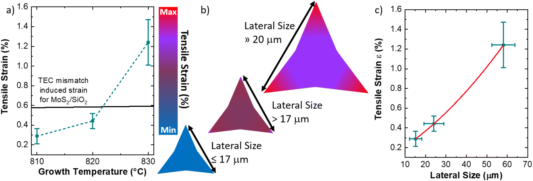 | ||
| Fig. 6 (a) Temperature dependent built-in strain values with a direct comparison with the theoretical TCE mismatch strain of the MoS2/SiO2 interface. (b) Sketch depicting the mechanism of the strain generation in the MoS2 ML with dependence on the flake size. (c) Dependence of the strain on the lateral size of the flake, reporting the polynomial fit. | ||
The dependence of the built strain as a function of the ML size is reported in Fig. 6c. The polynomial fitting reveals that the semi-empirical law of the average built-in strain as a function of the average size has parabolic behavior with the following parameters:
| εBuilt-in = A·d2 + B·d | (1) |
Conclusion
In conclusion, we demonstrate that the built-in strain of MoS2 monolayers, grown on a SiO2/Si substrate by liquid precursor chemical vapor deposition, is mainly dependent on the size of the monolayer. Using correlative analyses of AFM, TEM, Raman and PL, we are able to highlight an inconsistency in the number of layers in MoS2 flakes obtained by liquid precursor CVD. This leads to the identification of built-in strain dependent on the lateral size of MoS2 monolayers. The built-in strain values are close to the prediction of thermal expansion coefficient mismatch for monolayers with a lateral size less than than 20 μm. The built-in strain is drastically increased for 60 μm sized monolayers, leading to 1.2% tensile strain with a partial release of strain close to the monolayer triangular vertexes due to the formation of nanocracks. These results indicate that MoS2 monolayers, grown by liquid precursor CVD, can have a large built-in tensile strain when high growth temperatures (above 820 °C) are used to increase the monolayer size. A semi-empirical model is defined for the possible prediction of the expected built-strain for a certain lateral size of MoS2 monolayers without considering the possible release of strain due to the material cracking. The built-in strain dependence on the ML size and its inhomogeneity are tentatively attributed to the diffusion limited aggregation regime at high temperatures that gives rise to the fractal saw-toothed edges of the MoS2 monolayers.Experimental section
The chemicals composing the Mo liquid precursors were AMT (Sigma Aldrich purity 99.98%), NaOH (Carlo Erba) and Optiprep, an iodixanol based component provided by Serumwerk Bernburg AG normally employed in cell cultures.MoS2 flakes were synthesized under atmospheric pressure in an open tube using S powder with nitrogen as the carrier gas. The employed substrates were commercial 300 nm thick SiO2 coated highly conductive silicon wafer (Siltronic A.G.). Fig. S11† shows a schematic illustration of the CVD reactor, i.e. an open tube with a diameter of about 1 inch heated in a two-zone furnace. The sulfur boat is positioned in a low temperature zone (T = 180° C), while the growth substrate, after the spinning process of the Mo precursor solution, is placed in the high temperature zone (810 °C < T < 830 °C).77,78
AFM topography and phase maps were collected using a Bruker AFM operated in the scan assist mode. Scanning Raman and photoluminescence spectroscopy were carried out with a Renishaw InVia system, equipped with a confocal microscope, a 532 nm excitation laser and a 2400 line per mm grating (spectral resolution <1 cm−1). All the analyses were performed with an 100× objective (NA = 0.85), excitation laser power 500 μW, acquisition time 4 s for each spectrum and a pixel size of 1 μm × 1 μm. The Raman modes were fitted with a Lorentzian peak, except for the E2g mode of the specimen obtained at 830 °C that was fitted with a Voight peak due to the peculiar shape.
The statistical analysis involved analyzing twelve triangular structures, six measured by AFM and six measured by optical microscopy. The Raman scanning spectroscopic analysis was carried out on three different areas across the specimen.
Cross-sectional TEM analysis of a MoS2 flake grown at 830 °C was performed on a TEM-lamella prepared by a Zeiss Auriga Compact Focused Ion Beam (FIB) system. In order to protect the atomically thin layer of MoS2 from damage by the ion beam,79 the specimen was coated with amorphous carbon in a Balzers CED-010 setup prior to applying the standard procedure of FIB-lamella preparation. The lamella was then observed under a JEOL JEM 2200-FS microscope, operated at 200 kV.
We performed X-ray photoelectron spectroscopy (XPS) in an ultra-high-vacuum (UHV) chamber using a VSW HA100 hemispherical electron energy analyzer with a PSP power supply and control.80 We used a non-monochromatized Mg Kα X-ray source (photon at 1253.6 eV), with a final energy resolution at 0.86 eV. The Au 4f 7/2 peak at 84.0 eV has been used as calibration for the binding energy (BE) scale. Core level lineshape analysis has been performed using Voigt functions with a Gaussian to Lorentian ratio of 30%, after the subtraction of a Shirley background. The typical precision for each component's energy position was ±0.05 eV while for the area evaluation it was approximately ±2%.
Conflicts of interest
There are no conflicts to declare.Acknowledgements
The authors wish to thank Prof. R. Fornari (Department of Mathematical, Physical and Computer Sciences, University of Parma) for the useful discussion and support, Dr G. Attolini for his contribution during the CVD growth of MoS2 and Dr G. Bertoni (CNR-Nano, Modena) for his assistance in the carbon coating process prior to the TEM lamella preparation.References
- R. Roldán, A. Castellanos-Gomez, E. Cappelluti and F. Guinea, J. Phys.: Condens. Matter, 2015, 27, 313201 CrossRef PubMed.
- Z. Dai, L. Liu and Z. Zhang, Adv. Mater., 2019, 31, 1805417 CrossRef CAS PubMed.
- Z. Peng, X. Chen, Y. Fan, D. J. Srolovitz and D. Lei, Light: Sci. Appl., 2020, 9, 190 CrossRef CAS PubMed.
- G. H. Ahn, M. Amani, H. Rasool, D.-H. Lien, J. P. Mastandrea, J. W. Ager III, M. Dubey, D. C. Chrzan, A. M. Minor and A. Javey, Nat. Commun., 2017, 8, 608 CrossRef PubMed.
- S. Deng, A. V. Sumant and V. Berry, Nano Today, 2018, 22, 14–35 CrossRef CAS.
- L. Du, T. Hasan, A. Castellanos-Gomez, G.-B. Liu, Y. Yao, C. N. Lau and Z. Sun, Nat. Rev. Phys., 2021, 3, 193–206 CrossRef CAS.
- G. G. Naumis, S. Barraza-Lopez, M. Oliva-Leyva and H. Terrones, Rep. Prog. Phys., 2017, 80, 96501 CrossRef PubMed.
- J. Du, H. Yu, B. Liu, M. Hong, Q. Liao, Z. Zhang and Y. Zhang, Small Methods, 2021, 5, 2000919 CrossRef CAS PubMed.
- T.-J. Ko, M. Wang, C. Yoo, E. Okogbue, M. A. Islam, H. Li, M. S. Shawkat, S. S. Han, K. H. Oh and Y. Jung, J. Phys. D: Appl. Phys., 2020, 53, 313002 CrossRef CAS.
- Y. Qi, M. A. Sadi, D. Hu, M. Zheng, Z. Wu, Y. Jiang and Y. P. Chen, Adv. Mater., 2022, 2205714 Search PubMed.
- S. B. Desai, G. Seol, J. S. Kang, H. Fang, C. Battaglia, R. Kapadia, J. W. Ager, J. Guo and A. Javey, Nano Lett., 2014, 14, 4592–4597 CrossRef CAS PubMed.
- E. Blundo, M. Felici, T. Yildirim, G. Pettinari, D. Tedeschi, A. Miriametro, B. Liu, W. Ma, Y. Lu and A. Polimeni, Phys. Rev. Res., 2020, 2, 12024 CrossRef CAS.
- Y. Wang, C. Cong, W. Yang, J. Shang, N. Peimyoo, Y. Chen, J. Kang, J. Wang, W. Huang and T. Yu, Nano Res., 2015, 8, 2562–2572 CrossRef CAS.
- J. Feng, X. Qian, C.-W. Huang and J. Li, Nat. Photonics, 2012, 6, 866–872 CrossRef CAS.
- S. Z. Uddin, N. Higashitarumizu, H. Kim, I. K. M. R. Rahman and A. Javey, Nano Lett., 2022, 22, 5316–5321 CrossRef CAS PubMed.
- M. G. Harats, J. N. Kirchhof, M. Qiao, K. Greben and K. I. Bolotin, Nat. Photonics, 2020, 14, 324–329 CrossRef CAS.
- P. Hernández López, S. Heeg, C. Schattauer, S. Kovalchuk, A. Kumar, D. J. Bock, J. N. Kirchhof, B. Höfer, K. Greben, D. Yagodkin, L. Linhart, F. Libisch and K. I. Bolotin, Nat. Commun., 2022, 13, 7691 CrossRef PubMed.
- S. Bertolazzi, J. Brivio and A. Kis, ACS Nano, 2011, 5, 9703–9709 CrossRef CAS PubMed.
- Y. Yang, X. Li, M. Wen, E. Hacopian, W. Chen, Y. Gong, J. Zhang, B. Li, W. Zhou, P. M. Ajayan, Q. Chen, T. Zhu and J. Lou, Adv. Mater., 2017, 29, 1604201 CrossRef PubMed.
- A. Falin, M. Holwill, H. Lv, W. Gan, J. Cheng, R. Zhang, D. Qian, M. R. Barnett, E. J. G. Santos, K. S. Novoselov, T. Tao, X. Wu and L. H. Li, ACS Nano, 2021, 15, 2600–2610 CrossRef CAS PubMed.
- H. J. Conley, B. Wang, J. I. Ziegler, R. F. Haglund, S. T. Pantelides and K. I. Bolotin, Nano Lett., 2013, 13, 3626–3630 CrossRef CAS PubMed.
- K. He, C. Poole, K. F. Mak and J. Shan, Nano Lett., 2013, 13, 2931–2936 CrossRef CAS PubMed.
- A. Castellanos-Gomez, R. Roldán, E. Cappelluti, M. Buscema, F. Guinea, H. S. J. van der Zant and G. A. Steele, Nano Lett., 2013, 13, 5361–5366 CrossRef CAS PubMed.
- L. Mennel, V. Smejkal, L. Linhart, J. Burgdörfer, F. Libisch and T. Mueller, Nano Lett., 2020, 20, 4242–4248 CrossRef CAS PubMed.
- J. O. Island, A. Kuc, E. H. Diependaal, R. Bratschitsch, H. S. J. van der Zant, T. Heine and A. Castellanos-Gomez, Nanoscale, 2016, 8, 2589–2593 RSC.
- Y. Wang, C. Cong, C. Qiu and T. Yu, Small, 2013, 9, 2857–2861 CrossRef CAS PubMed.
- O. Çakıroğlu, J. O. Island, Y. Xie, R. Frisenda and A. Castellanos-Gomez, Adv. Mater. Technol., 2022, 2201091 Search PubMed.
- M. Zeng, J. Liu, L. Zhou, R. G. Mendes, Y. Dong, M.-Y. Zhang, Z.-H. Cui, Z. Cai, Z. Zhang, D. Zhu, T. Yang, X. Li, J. Wang, L. Zhao, G. Chen, H. Jiang, M. H. Rümmeli, H. Zhou and L. Fu, Nat. Mater., 2020, 19, 528–533 CrossRef CAS PubMed.
- W. Xu, T. Li, Z. Qin, Q. Huang, H. Gao, K. Kang, J. Park, M. J. Buehler, J. B. Khurgin and D. H. Gracias, Nano Lett., 2019, 19, 7941–7949 CrossRef CAS PubMed.
- W. Zheng, W. Huang, F. Gao, H. Yang, M. Dai, G. Liu, B. Yang, J. Zhang, Y. Q. Fu, X. Chen, Y. Qiu, D. Jia, Y. Zhou and P. Hu, Chem. Mater., 2018, 30, 6063–6070 CrossRef CAS.
- L. Cai, M. J. Shearer, Y. Zhao, Z. Hu, F. Wang, Y. Zhang, K. W. Eliceiri, R. J. Hamers, W. Yan, S. Wei, M. Tang and S. Jin, J. Am. Chem. Soc., 2018, 140, 10980–10987 CrossRef CAS PubMed.
- C. Choi, M. K. Choi, S. Liu, M. Kim, O. K. Park, C. Im, J. Kim, X. Qin, G. J. Lee, K. W. Cho, M. Kim, E. Joh, J. Lee, D. Son, S.-H. Kwon, N. L. Jeon, Y. M. Song, N. Lu and D.-H. Kim, Nat. Commun., 2017, 8, 1664 CrossRef PubMed.
- M. Vutukuru, H. Ardekani, Z. Chen, R. L. Wilmington, K. Gundogdu and A. K. Swan, ACS Appl. Nano Mater., 2021, 4, 8101–8107 CrossRef CAS.
- Q. Wang, J. Maisch, F. Tang, D. Zhao, S. Yang, R. Joos, S. L. Portalupi, P. Michler and J. H. Smet, Nano Lett., 2021, 21, 7175–7182 CrossRef CAS PubMed.
- C. Palacios-Berraquero, D. M. Kara, A. R.-P. Montblanch, M. Barbone, P. Latawiec, D. Yoon, A. K. Ott, M. Loncar, A. C. Ferrari and M. Atatüre, Nat. Commun., 2017, 8, 15093 CrossRef CAS PubMed.
- A. Branny, S. Kumar, R. Proux and B. D. Gerardot, Nat. Commun., 2017, 8, 15053 CrossRef CAS PubMed.
- A. Balgarkashi, V. Piazza, J. Jasiński, R. Frisenda, A. Surrente, M. Baranowski, M. Dimitrievska, D. Dede, W. Kim, L. Güniat, J.-B. Leran, A. Castellanos-Gomez, P. Plochocka and A. Fontcuberta i Morral, IEEE J. Quantum Electron., 2022, 58, 1–8 Search PubMed.
- J. Jasiński, A. Balgarkashi, V. Piazza, D. Dede, A. Surrente, M. Baranowski, D. K. Maude, M. Banerjee, R. Frisenda, A. Castellanos-Gomez, A. Fontcuberta i Morral and P. Plochocka, 2D Mater., 2022, 9, 45006 CrossRef.
- S. Kumar, A. Kaczmarczyk and B. D. Gerardot, Nano Lett., 2015, 15, 7567–7573 CrossRef CAS PubMed.
- S. Manzeli, A. Allain, A. Ghadimi and A. Kis, Nano Lett., 2015, 15, 5330–5335 CrossRef CAS PubMed.
- D. Lloyd, X. Liu, J. W. Christopher, L. Cantley, A. Wadehra, B. L. Kim, B. B. Goldberg, A. K. Swan and J. S. Bunch, Nano Lett., 2016, 16, 5836–5841 CrossRef CAS PubMed.
- F. Colangelo, A. Morandi, S. Forti, F. Fabbri, C. Coletti, F. V. Di Girolamo, A. Di Lieto, M. Tonelli, A. Tredicucci, A. Pitanti and S. Roddaro, Appl. Phys. Lett., 2019, 115, 183101 CrossRef.
- H. Kim, G. H. Ahn, J. Cho, M. Amani, J. P. Mastandrea, C. K. Groschner, D.-H. Lien, Y. Zhao, J. W. Ager, M. C. Scott, D. C. Chrzan and A. Javey, Sci. Adv., 2022, 5, eaau4728 CrossRef PubMed.
- Z. Liu, M. Amani, S. Najmaei, Q. Xu, X. Zou, W. Zhou, T. Yu, C. Qiu, A. G. Birdwell, F. J. Crowne, R. Vajtai, B. I. Yakobson, Z. Xia, M. Dubey, P. M. Ajayan and J. Lou, Nat. Commun., 2014, 5, 5246 CrossRef PubMed.
- K. Wang, A. A. Puretzky, Z. Hu, B. R. Srijanto, X. Li, N. Gupta, H. Yu, M. Tian, M. Mahjouri-Samani, X. Gao, A. Oyedele, C. M. Rouleau, G. Eres, B. I. Yakobson, M. Yoon, K. Xiao and D. B. Geohegan, Sci. Adv., 2023, 5, eaav4028 CrossRef PubMed.
- J. Wang, M. Han, Q. Wang, Y. Ji, X. Zhang, R. Shi, Z. Wu, L. Zhang, A. Amini, L. Guo, N. Wang, J. Lin and C. Cheng, ACS Nano, 2021, 15, 6633–6644 CrossRef CAS PubMed.
- T. H. Ly, S. J. Yun, Q. H. Thi and J. Zhao, ACS Nano, 2017, 11, 7534–7541 CrossRef CAS PubMed.
- W. H. Chae, J. D. Cain, E. D. Hanson, A. A. Murthy and V. P. Dravid, Appl. Phys. Lett., 2017, 111, 143106 CrossRef.
- L. Lei, Y. Lun, F. Cao, L. Meng, S. Xing, J. Guo, H. Dong, S. Gu, K. Xu, S. Hussain, Y. J. Li, Y. Sugawara, F. Pang, W. Ji, J. Hong, R. Xu and Z. Cheng, Nanotechnology, 2021, 32, 465703 CrossRef CAS PubMed.
- J. Li, M. Chen, C. Zhang, H. Dong, W. Lin, P. Zhuang, Y. Wen, B. Tian, W. Cai and X. Zhang, Adv. Mater., 2019, 31, 1902431 CrossRef PubMed.
- Y. Wan, H. Zhang, K. Zhang, Y. Wang, B. Sheng, X. Wang and L. Dai, ACS Appl. Mater. Interfaces, 2016, 8, 18570–18576 CrossRef CAS PubMed.
- H. Kim, G. H. Han, S. J. Yun, J. Zhao, D. H. Keum, H. Y. Jeong, T. H. Ly, Y. Jin, J.-H. Park, B. H. Moon, S.-W. Kim and Y. H. Lee, Nanotechnology, 2017, 28, 36LT01 CrossRef PubMed.
- Y.-H. Lee, X.-Q. Zhang, W. Zhang, M.-T. Chang, C.-T. Lin, K.-D. Chang, Y.-C. Yu, J. T.-W. Wang, C.-S. Chang, L.-J. Li and T.-W. Lin, Adv. Mater., 2012, 24, 2320–2325 CrossRef CAS PubMed.
- Y. Okuno, O. Lancry, A. Tempez, C. Cairone, M. Bosi, F. Fabbri and M. Chaigneau, Nanoscale, 2018, 10, 14055–14059 RSC.
- E. Rotunno, M. Bosi, L. Seravalli, G. Salviati and F. Fabbri, Nanoscale Adv., 2020, 2, 2352–2362 RSC.
- F. Giannazzo, M. Bosi, F. Fabbri, E. Schilirò, G. Greco and F. Roccaforte, Phys. Status Solidi RRL, 2020, 14, 1900393 CrossRef CAS.
- H. Li, Q. Zhang, C. C. R. Yap, B. K. Tay, T. H. T. Edwin, A. Olivier and D. Baillargeat, Adv. Funct. Mater., 2012, 22, 1385–1390 CrossRef CAS.
- C. Lee, H. Yan, L. E. Brus, T. F. Heinz, J. Hone and S. Ryu, ACS Nano, 2010, 4, 2695–2700 CrossRef CAS PubMed.
- C. Rice, R. J. Young, R. Zan, U. Bangert, D. Wolverson, T. Georgiou, R. Jalil and K. S. Novoselov, Phys. Rev. B: Condens. Matter Mater. Phys., 2013, 87, 81307 CrossRef.
- A. Michail, N. Delikoukos, J. Parthenios, C. Galiotis and K. Papagelis, Appl. Phys. Lett., 2016, 108, 173102 CrossRef.
- A. Michail, J. Parthenios, D. Anestopoulos, C. Galiotis, M. Christian, L. Ortolani, V. Morandi and K. Papagelis, 2D Mater., 2018, 5, 35035 CrossRef.
- G. Ciampalini, F. Fabbri, G. Menichetti, L. Buoni, S. Pace, V. Mišeikis, A. Pitanti, D. Pisignano, C. Coletti, A. Tredicucci and S. Roddaro, ACS Nano, 2022, 16, 1291–1300 CrossRef CAS PubMed.
- R. Rao, A. E. Islam, S. Singh, R. Berry, R. K. Kawakami, B. Maruyama and J. Katoch, Phys. Rev. B, 2019, 99, 195401 CrossRef CAS.
- B. Chakraborty, A. Bera, D. V. S. Muthu, S. Bhowmick, U. V. Waghmare and A. K. Sood, Phys. Rev. B: Condens. Matter Mater. Phys., 2012, 85, 161403 CrossRef.
- J.-Y. Lee, J. H. Kim, Y. Jung, J. C. Shin, Y. Lee, K. Kim, N. Kim, A. M. van der Zande, J. Son and G.-H. Lee, Commun. Mater., 2021, 2, 80 CrossRef CAS.
- G. Ye, Y. Gong, J. Lin, B. Li, Y. He, S. T. Pantelides, W. Zhou, R. Vajtai and P. M. Ajayan, Nano Lett., 2016, 16, 1097–1103 CrossRef CAS PubMed.
- F. Carrascoso, H. Li, R. Frisenda and A. Castellanos-Gomez, Nano Res., 2021, 14, 1698–1703 CrossRef.
- C. R. Zhu, G. Wang, B. L. Liu, X. Marie, X. F. Qiao, X. Zhang, X. X. Wu, H. Fan, P. H. Tan, T. Amand and B. Urbaszek, Phys. Rev. B: Condens. Matter Mater. Phys., 2013, 88, 121301 CrossRef.
- K. F. Mak, C. Lee, J. Hone, J. Shan and T. F. Heinz, Phys. Rev. Lett., 2010, 105, 136805 CrossRef PubMed.
- G. Plechinger, A. Castellanos-Gomez, M. Buscema, H. S. J. van der Zant, G. A. Steele, A. Kuc, T. Heine, C. Schüller and T. Korn, 2D Mater., 2015, 2, 15006 CrossRef.
- S. Cortijo-Campos, C. Prieto and A. De Andrés, Nanomaterials, 2022, 12 Search PubMed.
- C. Tsou, Y.-S. Huang, H.-C. Li and T.-H. Lai, Sens. Mater., 2005, 17, 441–451 CAS.
- L. Zhang, Z. Lu, Y. Song, L. Zhao, B. Bhatia, K. R. Bagnall and E. N. Wang, Nano Lett., 2019, 19, 4745–4751 CrossRef CAS PubMed.
- Y. Chen, W. Deng, X. Chen, Y. Wu, J. Shi, J. Zheng, F. Chu, B. Liu, B. An, C. You, L. Jiao, X. Liu and Y. Zhang, Nano Res., 2021, 14, 2314–2320 CrossRef CAS.
- S. Luo, C. P. Cullen, G. Guo, J. Zhong and G. S. Duesberg, Appl. Surf. Sci., 2020, 508, 145126 CrossRef CAS.
- S. Kataria, S. Wagner, T. Cusati, A. Fortunelli, G. Iannaccone, H. Pandey, G. Fiori and M. C. Lemme, Adv. Mater. Interfaces, 2017, 4, 1700031 CrossRef.
- I. Irfan, S. Golovynskyi, M. Bosi, L. Seravalli, O. A. Yeshchenko, B. Xue, D. Dong, Y. Lin, R. Qiu, B. Li and J. Qu, J. Phys. Chem. C, 2021, 125, 4119–4132 CrossRef CAS.
- L. Seravalli, M. Bosi, P. Fiorenza, S. E. Panasci, D. Orsi, E. Rotunno, L. Cristofolini, F. Rossi, F. Giannazzo and F. Fabbri, Nanoscale Adv., 2021, 3, 4826–4833 RSC.
- A. B. Andersen, A. Shivayogimath, T. Booth, S. Kadkhodazadeh and T. W. Hansen, Phys. Status Solidi, 2020, 257, 2000318 CrossRef CAS.
- R. Tatti, L. Aversa, R. Verucchi, E. Cavaliere, G. Garberoglio, N. M. Pugno, G. Speranza and S. Taioli, RSC Adv., 2016, 6, 37982–37993 RSC.
Footnote |
| † Electronic supplementary information (ESI) available. See DOI: https://doi.org/10.1039/d3nr01687k |
| This journal is © The Royal Society of Chemistry 2023 |