
 Open Access Article
 This Open Access Article is licensed under a
 Creative Commons Attribution 3.0 Unported Licence
Stable chemical enhancement of passivating nanolayer structures grown by atomic layer deposition on silicon†
Sophie L.
Pain
 *a,
Edris
Khorani
a,
Tim
Niewelt
abc,
Ailish
Wratten
a,
Marc
Walker
d,
Nicholas E.
Grant
a and
John D.
Murphy
*a
*a,
Edris
Khorani
a,
Tim
Niewelt
abc,
Ailish
Wratten
a,
Marc
Walker
d,
Nicholas E.
Grant
a and
John D.
Murphy
*a
aSchool of Engineering, University of Warwick, Coventry, CV4 7AL UK. E-mail: sophie.l.pain@warwick.ac.uk; john.d.murphy@warwick.ac.uk
bFraunhofer Institute for Solar Energy Systems ISE, Heidenhofstraße 2, 79110 Freiburg, Germany
cChair for Photovoltaic Energy Conversion, Institute for Sustainable Systems Engineering, University of Freiburg, Emmy-Noether-Straße 2, 79110 Freiburg, Germany
dDepartment of Physics, University of Warwick, Coventry, CV4 7AL UK
First published on 7th June 2023
Abstract
Incorporation of carrier-selective passivating contacts is on the critical path for approaching the theoretical power conversion efficiency limit in silicon solar cells. We have used plasma-enhanced atomic layer deposition (ALD) to create ultra-thin films at the single nanometre-scale which can be subsequently chemically enhanced to have properties suitable for high-performance contacts. Negatively charged 1 nm thick HfO2 films exhibit very promising passivation properties – exceeding those of SiO2 and Al2O3 at an equivalent thickness – providing a surface recombination velocity (SRV) of 19 cm s−1 on n-type silicon. Applying an Al2O3 capping layer to form Si/HfO2/Al2O3 stacks gives additional passivation, resulting in an SRV of 3.5 cm s−1. Passivation quality can be further improved via simple immersion in hydrofluoric acid, which results in SRVs < 2 cm s−1 that are stable over time (tested for ∼50 days). Based on corona charging analysis, Kelvin probe measurements and X-ray photoelectron spectroscopy, the chemically induced enhancement is consistent with changes at the dielectric surface and not the Si/dielectric interface, with fluorination of the Al2O3 and underlying HfO2 films occurring after just 5 s HF immersion. Our results show that passivation is enhanced when the oxides are fluorinated. The Al2O3 top layer of the stack can be thinned down by etching, offering a new route for fabrication of ultra-thin highly passivating HfO2-containing nanoscale thin films.
Introduction
Crystalline silicon (c-Si) is the most successful photovoltaics technology to date accounting for >95% of solar cells currently produced.1 Passivating films play an essential role in limiting charge carrier recombination at surfaces, hence increasing effective charge carrier lifetimes and solar cell efficiencies. Surface passivation is realized by a combination of chemical passivation of dangling bonds and field effect passivation to repel charge carriers away from the interface. Surface passivation quality can be quantified in terms of a surface recombination velocity (SRV) defined as: | (1) |
 | (2) |
For surface passivation of optically exposed regions of solar cells, it is common to use relatively thick (10 to 100 nm) passivating films which can also serve as antireflection coatings, and these may be single dielectric layers or stacks of multiple materials. A more innovative application of passivation layers is in carrier-selective contact structures.3 In this context, the passivating layer or layer stacks must be ultra-thin (typically < 5 nm) to mitigate a significant increase in the series resistance of the device. To date, the record power conversion efficiency achieved by a single-junction silicon solar cell is a silicon heterojunction (HJT) based solar cell that incorporates ultra-thin (∼5 nm) intrinsic a-Si:H as the passivating interlayer.4 SiOx based passivating contacts, including the Tunnel Oxide Passivated Contact (TOPCon) and Poly-Silicon on Oxide (POLO), have also demonstrated a high potential in recent years.5,6
Passivating dielectric thin films can be grown via chemical vapour deposition (CVD), thermal oxidation, sputtering, and atomic layer deposition (ALD).7 ALD is based on sequential self-terminating reactions8 and offers Angstrom-scale thickness control with a high degree of uniformity and conformality, even for complex surface geometries.9 Passivated emitter and rear cell (PERC) photovoltaics are the current industry standard and can often incorporate ALD-grown Al2O3 films.10 Al2O3 films possess negative fixed charges (∼1012–1013 q cm−2),11,12 in contrast to many other dielectric passivating layers, such as SiNx, which are positively charged.7 Al2O3 passivates extremely well when relatively thick (>10 nm) but passivates poorly when thin (<1 nm).13 There is a strong motivation to develop dielectrics with thicknesses at the single nanometre scale which also passivate well for new passivating contact structures.
Recent studies have identified HfO2 as a versatile negatively charged passivating layer which can be grown by ALD.14,15 For relatively thick passivation layers (5 to 25 nm), passivation from HfO2 is not competitive with that from Al2O3, with typical SRVs being ∼5 cm s−1 (ref. 14 and 16) and <1 cm s−1,17 respectively. We have recently studied passivation by ultra-thin HfO2 films and determined SRVs < 2.5 cm s−1 for 2.2–3.3 nm thick films, with a negative fixed charge density on the order ∼1012 q cm−2.13 Although this is promising and better than Al2O3 of similar thickness, when the HfO2 thickness is reduced to ∼1 nm – as required for passivating contacts – the SRV is ∼19 cm s−1. Work in this current paper aims to enhance this.
One widely used approach for enhancing the passivation of dielectrics is to apply capping layers. Positively charged SiNx provides SRVs < 6 cm s−1 and surface recombination current densities (J0,s, an alternative measure of passivation2,18) < 5 fA cm−2 when capped with SiOx,19,20 and SRVs < 3 cm s−1 when capped with Al2O3.21 Recent results by Kersten et al. demonstrate that SiNx capping layers incorporated into industrial PERC cells allow cell efficiencies of 23.7% to be achieved.22 SiNx capping layers are often grown via plasma-enhanced CVD on top of thermal SiOx or ALD-grown Al2O3. Preparing a stacked dielectric structure via a single growth method rather than two allows for more streamlined industrial production. Negatively charged Al2O3 has been identified as a promising capping layer for SiO2,23 ZnO,24 and HfO2.25,26 Al2O3 capping layers are thought to boost passivation by affecting hydrogen availability – either as a source or by preventing H effusion.23,24,27,28
In this paper, we develop passivating stacks grown solely via ALD and assess the viability of Al2O3 as a capping layer for nanolayer HfO2. We subsequently apply various wet chemical treatments as we observed improvement in nanolayer dielectrics in previous studies.29 We also find that it is possible to thin-down the Al2O3 capping layer chemically, providing a new route to fabricating enhanced ultra-thin HfO2 passivating films.
Results and discussion
Stacks involving ultra-thin (1 nm) HfO2 interlayers
To determine the viability of Al2O3 capping layers for nanolayer HfO2, three film structures were deposited at 200 °C onto 5 Ω cm 125–150 μm thick n-type Cz silicon wafers: (1) 1 nm HfO2 (10 ALD cycles, denoted Si/HfO2. The growth rate of HfO2 under the conditions used in this work was characterised in our previous work13); (2) 1 nm HfO2 capped with 30 nm Al2O3 (250 ALD cycles, denoted Si/HfO2/Al2O3); and (3) 30 nm Al2O3 (denoted Si/Al2O3). Samples were annealed (“activated”) in air ambient in a tube furnace at temperatures between 350–600 °C for 30 min to improve the passivation. The passivation quality of both HfO2 and Al2O3 are known to be dependent on annealing temperature, with optimal passivation achieved in both cases on annealing at 450–500 °C.11,30 Photoconductance decay lifetime curves for the three structures activated at 450 °C are shown in Fig. 1(a). SRVs defined according to eqn (1) at Δn = 1 × 1015 cm−3 are plotted as a function of activation temperature in Fig. 1(b). | ||
| Fig. 1 (a) Effective lifetime curves for 1 nm Si/HfO2 (orange squares), 30 nm Si/Al2O3 (green circles), Si/HfO2/Al2O3 (purple triangles) stacks with 1 nm HfO2 and 30 nm Al2O3 activated at 450 °C. Also shown is the intrinsic lifetime limit.31 Data for Si/HfO2 were published previously.13 Substrates are high quality, ∼150 μm thick, (100) orientation, 5 Ω cm, chemically etched n-type Cz silicon wafers. Samples with 1 nm HfO2 were deposited onto n-type silicon from a nominally identical batch, excepting a reduced thickness of ∼125 μm. (b) SRV determined at Δn = 1 × 1015 cm−3 for the same three configurations as in (a), with the same symbols used. The shaded regions correspond to the relative measurement uncertainty. No data in this figure arose from chemically treated samples. | ||
The data in Fig. 1 for n-type Si confirm that thick Al2O3 provides better passivation than thin HfO2, and that depositing 30 nm of Al2O3 on top of the HfO2 has a significant positive impact on effective lifetime and hence passivation level. For activation annealing at 450 °C, an upper limit SRV of 18.6 cm s−1 is found for thin HfO2. Deposition of a 30 nm Al2O3 capping layer results in significant improvement, reducing SRV to 3.5 cm s−1. The passivation achieved here for Si/HfO2/Al2O3 is an order of magnitude better than previous reports26 and corresponds to a single-side J0,s of 23.4 fA cm−2. It is noted that a lower SRV (of 0.8 cm s−1) is achieved for 30 nm Al2O3 alone. In the ESI (Fig. S1†), we show results for p-type Ga-doped silicon (same thickness and resistivity) and also find improvement upon deposition of a capping layer on 1 nm of HfO2 on p-type silicon.
The improved passivation observed with Si/HfO2/Al2O3 is in keeping with the reports of Polzin et al. and Dingemans et al., who observe that an Al2O3 capping layer improves passivation for TOPCon and SiO2 structures, respectively.27,28 The increased passivation is often attributed to the presence of hydrogen originating from the dielectric passivating the Si interface, hence reducing Dit.33,34 Oudot et al. also report improved chemical passivation on depositing HfO2 atop thermal SiO2, which they link to hydrogen diffusing to the Si/dielectric interface and passivating dangling bonds.35 We would not expect any improvement in field-effect passivation from the applied Al2O3 capping layer, based on reports of HfO2 acting as an “inert spacer” once Al2O3 is deposited upon it.25
HF treatments of stacks with different HfO2 interlayer thicknesses
We next present results which show the impact of HF-based chemical treatments on the passivation. It is known that Al2O3 capping layers for poly-Si can be removed without sacrificing passivation quality.24,33,34,36 Interestingly, we find here that partially removing Al2O3 films with dilute HF has a considerable positive impact on the surface passivation. Fig. 2(a) shows the effect of 5 s immersion in 1% HF on SRV for Si/HfO2/Al2O3 stacks with 1 nm HfO2 grown on n-type Si activated at different temperatures. The HF treatment provides a substantial increase in passivation level for all activation temperatures, with SRVs < 2 cm s−1 and single-side J0,s of ∼11.6 fA cm−2 at 450 °C. The corresponding lifetime curves in Fig. 2(b) show no significant change in injection dependence (and hence passivation mechanism) following immersion. A similar increase occurs with Si/HfO2/Al2O3 on p-type Si with a 5 s HF immersion which leads to a 1 cm s−1 SRV reduction as shown in Fig. S1.† | ||
| Fig. 2 (a) SRVs for Si/HfO2/Al2O3 as-annealed (purple triangles) and following 5 s in HF (yellow triangles) as a function of annealing temperature. The shaded regions correspond to the relative uncertainty of SRV. (b) Effective lifetime curves for 1 nm Si/HfO2 (orange squares) and Si/HfO2/Al2O3, as-annealed at 450 °C (purple triangles) and following 5 s immersion in HF (yellow triangles). (c) Effective lifetime curves for 10 nm Si/HfO2 (orange diamonds) and Si/HfO2/Al2O3, as-annealed at 450 °C (purple triangles) and following 5 s immersion in HF (yellow triangles). Also shown is the intrinsic lifetime limit.31 All effective lifetime data are the average of five measurements and are assumed to be accurate to ±8%.32 | ||
Si/HfO2/Al2O3 stacks incorporating HfO2 layers of a more conventional thickness (10 nm, 100 ALD cycles) were also studied, with lifetime curves shown in Fig. 2(c). The passivation achieved for such stacks is similar to that with uncapped 10 nm Si/HfO2 (average SRVs (single-side J0,s) of 5.8 (19.6) versus 5.7 cm s−1 (27.5 fA cm−2) for uncapped and capped 10 nm Si/HfO2, respectively). This implies that the beneficial impact of the capping layer is less pronounced for thicker HfO2 layers. Nevertheless, as shown in Fig. 2(c), 5 s HF immersion also enhances lifetime for these stacks, with a decrease in average SRV (single-side J0,s) from 5.7 (27.5) to 3.6 cm s−1 (16.7 fA cm−2). We also investigated reversing the stack structure, using 10 nm HfO2 to cap 30 nm Al2O3. For this case, there is no significant improvement in passivation on application of the capping layer as shown in Fig. S2.†
Stability of enhanced passivation
For this chemical treatment step to be useful for photovoltaics or other devices, its effects must be stable with time and tolerant to subsequent processing at elevated temperatures. Earlier studies into HfO2 passivation stated that for HfO2-based layers to be incorporated into photovoltaic processing schemes, the temperatures they were exposed to could not exceed 400 °C.16 We have since shown that HfO2-based films perform well up to ∼500 °C,30 but, nevertheless 400–500 °C temperature range provides a useful benchmark for testing thermal stability.To assess temporal stability, samples were stored in a sealed Petri dish in ambient environment following HF immersion, and passivation quality was monitored at regular intervals. These results, relative to an untreated stack, are shown in Fig. 3(a). It is evident that the lifetime enhancement achieved with 1% HF is stable for at least 50 days, with no degradation onset observed. This stability far exceeds that of HF or other acidic treatment of bare silicon.37,38
 | ||
| Fig. 3 (a) SRVs determined for Si/HfO2/Al2O3 with 1 nm HfO2 with no chemical treatment (purple triangles) and HF-dipped stacks (yellow triangles) as a function of time exposed to ambient conditions. Average SRVs (left axes) and corresponding single-side J0,s values (right axes) for parallel samples of Si/HfO2/Al2O3 with (b) 1 nm and (c) 10 nm HfO2 deposited on 5 Ω cm 150 μm n-type c-Si with no chemical treatment (purple triangles) and following 5 s immersion in 1% HF (yellow triangles). Effective lifetime (from which SRV is extracted at Δn = 1 × 1015 cm−3) was measured following re-annealing at temperatures between 50–450 °C for 30 min and reported SRV corresponds to the average of two parallel samples. In all cases, effective lifetime values (from which SRV is extracted) were the average of five measurements, and shaded regions correspond to relative uncertainty of SRV. Connections between the data points serve as a guide to the eye. | ||
Fig. 3(b) shows SRVs for Si/HfO2/Al2O3 stacks with 1 nm HfO2 activated at 450 °C and sequentially re-annealed in air in a tube furnace for 30 min at temperatures increasing in 50 °C intervals. The two leftmost datapoints (at the 25 °C ‘re-anneal’ temperature) for HF-dipped Si/HfO2/Al2O3 with 1 nm HfO2 (yellow triangles) correspond to the average SRV before and after HF immersion. Both the HF-dipped stack and the untreated reference sample show a steady increase in SRV with re-annealing up to a temperature of 250 °C. We then observe a sharp increase in the SRV when re-annealing at 300 and 350 °C. For higher annealing temperatures, we observe a recovery of passivation (decrease in SRV). The average passivation quality of HF-dipped stacks exceeds that of untreated Si/HfO2/Al2O3 at all temperatures studied. Higher temperature ranges could not be studied, as above ∼500 °C, HfO2-based passivation quality is known to degrade,30 and hence it would not be possible to separate contributions from the dielectric layers and the chemical treatment at these annealing temperatures.
The same experiment was conducted on Si/HfO2/Al2O3 stacks with 10 nm HfO2, with the data shown in Fig. 3(c). A trend broadly similar to the 1 nm HfO2 case is found although following re-annealing at 300 °C, untreated stacks show slightly better passivation quality than HF-dipped stacks. The trends observed in SRV and J0,s are mirrored in the effective lifetime data from which these values were determined (Fig. S3†). As both J0,s and SRV describe surface recombination, the correlation between the extracted surface parameters and the overall effective lifetime further confirms this variation is surface-related, rather than bulk-related. Although the SRV equation assumes no change in bulk lifetime, J0,s makes no such assumption.
Similar experiments exploring the impact of subsequent re-anneals on uncapped Si/HfO2 with 1 and 10 nm HfO2 were also conducted, with results shown in Fig. S4 and S5,† respectively, demonstrating comparable trends. As the degradation–recovery cycle is observed for both thin and thick stacks, as well as uncapped thin and thick HfO2, it is clearly neither caused by specific HfO2 thickness nor by the stack architecture. Indeed, it is known to occur for other dielectrics, as a similar ‘re-activation’ can be seen with SiO2, whereby high temperature processing reduces surface passivation, but it is recovered with subsequent annealing at 400 °C.21 The origins of this recovery in passivation at 400–450 °C are not fully clear. It could be associated with release of bound hydrogen within the passivation layers, which is mobile at these temperatures39 or to short-range rearrangements of bonds ‘re-activating’ the passivation, an effect also observed for Si/SiNx/Al2O3 stacks.28 Many industrial photovoltaic processing steps involve temperatures far above those considered in this study (although for shorter durations of time),10,21,40 but the tolerance of the stacks and even the wet chemical improvement discussed here to extended subsequent thermal processing is encouraging.
The passivation qualities achieved here are greater for Si/HfO2/Al2O3 stacks with thin versus thicker HfO2 and given the considerable recent interest in developing ultra-thin dielectrics as passivating interlayers or components of passivating contacts,41–43 the majority of this article will focus on Si/HfO2/Al2O3 stacks with thin (1 nm) HfO2.
Electronic origins of improved passivation
It is important to establish whether the origin of the HF-induced improvement in passivation is due to changes at the silicon/dielectric interface and/or changes at the dielectric/air interface. Therefore corona charging was employed to determine the charge fixed in the films and the level of chemical passivation at the silicon–dielectric interface.44 Successive corona charging was applied, with the quantity of charge (Qcorona) required to minimise τeffective indicative of Qfixed within the film.Typical τeffectiveversus Qcorona curves for chemically treated Si/HfO2/Al2O3 stacks activated at different temperatures are shown in Fig. 4(a). Data for untreated stacks can be found in Fig. S6.† The extracted Qfixed and τminimum values are shown in Fig. 4(b) and (c), respectively, for untreated stacks and those which had been subjected to a 5 s dip in HF. These respective quantities represent a measure of the charge in the films and the chemical passivation level.
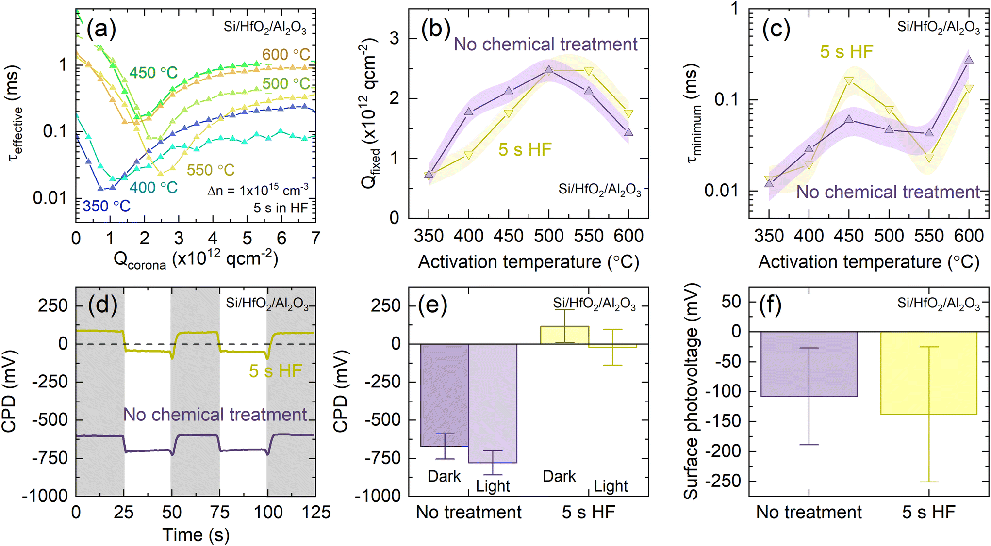 | ||
| Fig. 4 (a) Effective lifetime as a function of Qcorona for Si/HfO2/Al2O3 stacks with 1 nm HfO2 activated at temperatures between 350–600 °C and immersed in HF for 5 s. (b) Qfixed and (c) τminimum as a function of activation annealing temperature for Si/HfO2/Al2O3 both untreated (purple) and following a HF dip (yellow). Shaded regions in (b) and (c) correspond to measurement uncertainty. Error bars in (b) correspond to a Qcorona of 1.85 × 10¹¹ q cm−2, 50% of Qcorona deposited in each charging step. Shaded regions in (c) correspond to experienced variation in effective lifetimes between Si/HfO2/Al2O3 stacks. Connections between data points serve as a guide to the eye. (d) Representative surface photovoltage measurements, used to determine (e) CPD under dark conditions and illumination, and (f) SPV for both untreated stacks (purple) and stacks following a HF dip (yellow). Samples were activated at 450 °C. For each sample, at least five locations are measured in duplicate, and the reported values are the average of each point, with the CPD determined the mean of two darkness-illumination measurement cycles. The error bars are the mean standard deviation of these measurements. | ||
In the case of stacks that were not chemically treated, a clear dependence of Qfixed on activation temperature is apparent, consistent with the behaviour of uncapped HfO2 films. The best passivation is observed for films activated at 450–500 °C, as is evident from Fig. 1, at which temperatures we observe Qfixed of 2.5 × 10¹² q cm−2. This is lower than values observed for Si/HfO2 or Si/Al2O3,11–13 but is consistent with reported interface fixed charge densities determined with capacitance–voltage (C–V) measurements for Si/HfO2/Al2O3.25 Extracted Qfixed and τminimum for parallel samples of both untreated and HF-dipped Si/HfO2/Al2O3 stacks are, broadly speaking, in agreement, as shown in (b) and (c).
The absence of any definitive change in Qfixed or τminimum with HF treatment suggests that the factors contributing to the observed improvement in passivation are on the sample surface, rather than arising from changes at the Si/dielectric interface. This contrasts with the alneal process,45,46 whereby direct improvements are made to the Si/dielectric interface through use of an Al layer which is a considerable distance from the interfacial region.
Passivating stacks were also characterised by Kelvin probe to provide an understanding of changes at the dielectric/air interface upon HF-based treatment. The contact potential difference (CPD) is strongly dependent on the presence of charge on the dielectric surface.47Fig. 4(d) shows representative CPD data for Si/HfO2/Al2O3 (untreated and HF-dipped) collected under a cycle of dark conditions (shaded regions) and under illumination (non-shaded regions). The absolute value of CPD increases after HF immersion, but as shown in Fig. 4(e), the magnitude of CPD change is consistent between stacks which were and were not treated with HF.
The surface photovoltage (SPV), which is the change in CPD upon illumination, can be used to assess the charge polarity in the dielectric stack, with a negative SPV expected for a negatively charged film.48Fig. 4(f) shows that the SPV magnitude is consistent between samples with and without HF treatment, demonstrating that the treatment does not modify the charge polarity or magnitude. Although SPV magnitude relates to charge magnitude, accurately quantifying charge levels based on SPV is non-trivial,48 as SPV can be highly variable and dependent on material properties and surface defects.49,50 The SPV determined before and after HF treatment are of a similar magnitude, and within the experienced intra-sample variation. Importantly, in all cases the measured SPV was negative, demonstrating that the negative charge polarity is unchanged on treatment.
Changes in CPD that do not affect SPV shifts, as observed here, are reported to be associated with surface dipoles,48,51 which could be a potential contributor to the improved passivation following HF immersion. A shift in CPD without an accompanying shift in SPV has also been observed for n-type Si treated with benzoquinone-methanol and was attributed to differing surface dipoles before and after treatment.52 In particular, Yang et al., who observe similar trends, attribute these to the presence of positive charges adsorbed onto the negatively charged surface (cf. our Al2O3 film), forming an interfacial dipole.53
Some extrinsic passivation mechanisms, such as corona charging of dielectrics, can be removed by rinsing with deionised (DI) water54 unless additional protective coatings are applied.55 To assess whether the extrinsic passivation achieved here can be similarly removed, a Si/HfO2/Al2O3 sample was immersed in DI water immediately after 5 s HF immersion. Data shown in Fig. S7† demonstrate no significant change in passivation quality on rinsing, as SRVs < 2 cm s−1 are achieved after a HF dip whether or not it is preceded by a DI water rinse, suggesting that the enhancement is resistant to further solution processing. KP results also show an increase in CPD which is not associated with a change in SPV, similar to that following HF immersion alone, suggesting that the surface dipoles inferred from KP persist after rinsing.
The enhancement observed here with Si/HfO2/Al2O3 differs from reports of Si/SiO2/Al2O3, where there is no notable change in passivation on removing the sacrificial Al2O3 capping layer.33,34,36 This implies that this improvement may be specific to the HfO2 or Al2O3 layers used – or even to the full Si/HfO2/Al2O3 stack. To assess this, we investigated the effect of 5 s HF immersion on single layer Si/HfO2 and Si/Al2O3 samples. The layers were 1 and 30 nm thick respectively, to allow direct comparison with the behaviour of Si/HfO2/Al2O3 stacks. No change in passivation quality was observed for Si/Al2O3, with SRVs of 1.1 cm s−1 achieved both prior to and following the treatment. Effective lifetime data for this test can be found in Fig. S8.† In order to probe whether the high-quality passivation achieved with Al2O3 had potential for improvement with HF, samples with lower quality Al2O3 passivation were subjected to the same HF treatment, and no improvement in passivation was observed. Immersing Si/HfO2 into 1% HF for 5 s was sufficient to remove the passivation (and the HfO2 layer, as confirmed with XPS) completely. Rather than the increase in passivation quality (decreasing SRV) observed for Si/HfO2/Al2O3, immersion of Si/HfO2 results in an immeasurably high SRV. Thus, the observed improvement seems related to properties of the complete stack, not the individual layers. Changes in CPD could also be due to changes in the dielectric constant,30 but this does not seem likely for a simple room temperature chemical treatment.
Although our experimental data suggest that the enhanced passivation is related to a charging effect at the dielectric surface, we cannot rule out the role of hydrogen and its ability to passivate the silicon–dielectric interface as an alternative explanation. In this case, the observed improvement in passivation following removal of the Al2O3 capping layer is similar to the “alneal” process, whereby Si/SiO2 interfacial passivation is improved by depositing a sacrificial Al layer.45,46 Improved passivation following an alneal is reported to be due to Al catalysing production of atomic hydrogen,56 or H2 generation within the interfacial AlOx film which forms between the Si and the Al, passivating the interface.27 This process improves interfacial Si/dielectric passivation, even though the Al layer is tens of nanometres away from this interface, similar to the stack structures we use. Nevertheless, our electrical characterisation suggests that this is unlikely in our case.
Chemical analysis of HF-treated stacks and correlation with lifetime changes
We next perform experiments to assess the chemical composition of HF-treated Si/HfO2/Al2O3 stacks. Fig. 5(a) shows XPS spectra for such stacks with 1 nm of HfO2 immersed in HF for various times (up to 45 s), together with an untreated control. Prior to the HF treatment, the XPS spectrum is dominated by Al 2p and Al 2s peaks at ∼75 eV and ∼120 eV, respectively.57 No core levels corresponding to hafnium are detected (e.g., Hf 4f would be expected at ∼17 eV for HfO2![[thin space (1/6-em)]](https://www.rsc.org/images/entities/char_2009.gif) 58), which is unsurprising given that the Al2O3 capping layer thickness (∼30 nm) greatly exceeds the XPS photoelectron sampling depth (10 nm for hafnium 4f photoelectrons through an Al2O3 overlayer).59,60
58), which is unsurprising given that the Al2O3 capping layer thickness (∼30 nm) greatly exceeds the XPS photoelectron sampling depth (10 nm for hafnium 4f photoelectrons through an Al2O3 overlayer).59,60
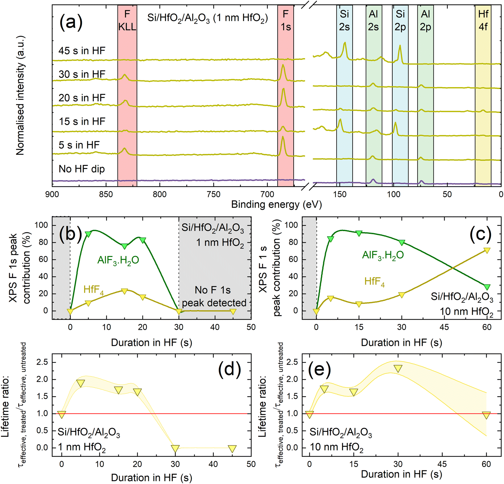 | ||
| Fig. 5 (a) XPS survey scans for different HF immersion durations, with key XPS core levels identified. The small XPS contribution at ∼110 eV visible after 30 s immersion corresponds to a plasmon loss feature for Si 2p, rather than an Al 2p signal. The separation between the main photoelectron peak and this bulk plasmon peak (and that of the Si 2s signal and its neighbouring satellite peak) of ∼18 eV is consistent with reported plasmon loss signals.63,64 (b) and (c) Evolution of HfF4 (yellow) and AlF3·H2O (green) contribution to F 1s peak for Si/HfO2/Al2O3 with 1 nm HfO2 (b) and 10 nm HfO2 (c) as a function of time in 1% HF. Lifetime enhancement as a function of immersion time of Si/HfO2/Al2O3 stacks in 1% HF, determined as τeffective, treated/τeffective, untreated for stacks with 1 nm HfO2 in (d) and 10 nm HfO2 in (e). Effective lifetime was extracted at Δn = 1 × 1015 cm−3. Each point was the average of five measurements and has an assumed uncertainty of ±8%.32 The lines between data points in (b)–(e) serve as a guide to the eye. | ||
Since HF is known to etch Al2O3,61 increasing the HF dip duration will also increase the amount of Al2O3 removed. We determine the etch rate of Al2O3 in 1% HF as 1 nm s−1 (shown in Fig. S9†). Measured thickness across a sample following 5 s immersion in HF had a standard deviation of 2.3 nm (compared to 0.5 nm on non-HF dipped samples), suggesting that the capping layer is not etched uniformly in HF.
The XPS spectrum in Fig. 5(a) after 5 s in HF is consistent with the Al2O3 still being present, and the only notable change is the appearance of F peaks at ∼685 eV and ∼820 eV. Closer inspection of the F 1s core level at ∼685 eV allows deconvolution into two components, as shown in Fig. S10,† with the main contribution at ∼686.4 eV corresponding to AlF3·H2O, and another smaller contribution at ∼685.4 eV corresponding to HfF4.57 It is surprising that hafnium-related signals are seen in XPS after relatively short HF immersion times when an intact Al2O3 capping layer is expected to remain. One explanation is the possible existence of pinholes in the Al2O3 layer which are widened by HF etching thus exposing the HfO2 layer beneath. A similar observation was reported by Cheng et al., who report pinholes in Al2O3 capping layers which are widened by an etching solution.62
The relative HfF4 and AlF3·H2O contributions as determined by deconvoluting F 1s peak intensity as a function of HF immersion time are shown for stacks with 1 nm and 10 nm HfO2 interlayers in Fig. 5(b) and (c), respectively. The corresponding lifetime enhancements relative to the untreated values are shown in Fig. 5(d) and (e). The impact of the HF treatment on passivation level varies with HfO2 interlayer thickness. For 1 nm HfO2 interlayers, the AlF3·H2O XPS signal contribution in Fig. 5(b) has a similar dependence on HF immersion time to the lifetime enhancement shown in Fig. 5(d). It could therefore be that the passivation enhancement relates to the extent of fluorination of the Al2O3 layer and the proportion of AlF3·H2O present. Interestingly when the dielectrics are reversed, Si/Al2O3/HfO2 with 10 nm HfO2 shows no improvement in passivation with HF immersion and also no F signals are observed in the XPS spectra (Fig. S11†).
The top layer of our conventional stacks is ∼30 nm of Al2O3, thus 30 s in 1% HF should be sufficient to remove the Al2O3 layer. Indeed, XPS analysis of an Si/HfO2/Al2O3 stack with a 1 nm HfO2 interlayer after 30 s in HF, shown in Fig. 5(a), demonstrates that no Hf or Al peaks remain, while strong peaks are present from the silicon substrate. Data for stacks with 1 nm HfO2 interlayers in Fig. 5(b) are only plotted for the first 20 s of HF immersion, after which XPS results indicate that the oxides have been etched away entirely. This is consistent with the lifetime data shown in Fig. 5(e) which show passivation is lost for these immersion times.
For 10 nm HfO2 interlayers, the passivation quality of stacks is dependent on HF immersion time, as shown in Fig. 5(e). Stacks with thicker HfO2 layers can be subjected to HF dips of up to 30 s with the passivation remaining enhanced. Corresponding lifetime curves are shown in Fig. S12.† The variation in passivation enhancement with 10 nm HfO2 interlayers correlates with the variation in the HfF4 signal up to 30 s, and the AlF3·H2O contribution after 30 s. From this it appears that the lifetime variation is related to fluorination of the dielectric layers. Beyond 30 s in HF, enhancements are lost, but the resulting effective lifetimes remains similar to the original level.
The difference in behaviour for ≥30 s of HF immersion for 1 nm and 10 nm interlayers is likely because of differences in crystallisation level between the HfO2 films of different thicknesses. 10 nm thick films are known to crystallise upon annealing at 450 °C,30 becoming highly resistant to etching in HF.65 ∼1 nm HfO2 films are unlikely to crystallise fully without being annealed at 700–800 °C,66 and thus have not developed resistance to etching in HF.
A key aim of this work is developing enhanced ultra-thin passivating layers which have potential for passivating contacts. These passivating layers need to have low J0,s,67 with good passivating contacts/interlayers generally having J0,s values ≪10 fA cm−2,67,68 as well as film thicknesses ideally ≪5 nm.67,69 On this front, the most promising sample is Si/HfO2/Al2O3 with 1 nm HfO2 following 20 s HF immersion. By this point, approximately 20 nm of Al2O3 has been etched, resulting in a ∼11 nm Si/HfO2/Al2O3 stack with enhanced passivation. An SRV of 1.5 cm s−1 is achieved, corresponding to a single-side J0,s of 5.8 fA cm−2, which, to the best of our knowledge, is the first time a J0,s value ≪10 fA cm−2 has been measured for a HfO2-based film. The passivation quality achieved here is well within the target for passivating contact materials and structures. The stack thickness (∼11 nm) is not yet in the thickness range for passivating contacts or interlayers, but an optimised etching duration would provide thinner stack thicknesses. We have demonstrated that applying a capping layer and chemically thinning it provides a potential new route for fabrication of ultra-thin highly passivating nanoscale thin films.
Treatment of stacks with other chemical solutions
Chemical treatments other than HF were applied to Si/HfO2/Al2O3 stacks to help elucidate the mechanisms of passivation enhancement. Stacks were treated for 5 s in either 1% HCl or SC1 (“Standard Clean 1”, a hot (80 °C) mixture of NH4OH, H2O2 and H2O in a 1:1:5 ratio). These solutions, both a key part of industrial silicon cleaning and processing,70 were selected as HCl is a protic acid (stronger than HF) but does not etch Al2O3, whilst SC1 is alkaline but etches Al2O3.61
Fig. 6(a) shows relative lifetime changes following treatment in HF, SC1, and HCl. As was the case for data in Fig. 3(a), samples were stored in a sealed Petri dish in ambient conditions, with passivation quality monitored at regular intervals. All three solutions enhance lifetime, but none are as stable as HF. The lifetime enhancement with HCl degrades within two weeks, eventually returning to the effective lifetime achieved prior to the HCl dip. The passivation gain with SC1 degrades considerably after one week, with a more gradual decay after this point. We also checked whether a DI water treatment influences passivation quality, but effective lifetime curves shown in Fig. S13† show this is not the case, hence it is the solute (not the common water solvent) which changes the passivation. SC1 is non-acidic, demonstrating that the protic nature of HF is not solely responsible for the improved passivation. Also, HCl does not etch Al2O3, so the enhancement is not due to etching alone. KP analysis presented in Fig. S14† demonstrates shifts in CPD which are not reflected in comparable shifts in SPV, supporting our surface dipole hypothesis.
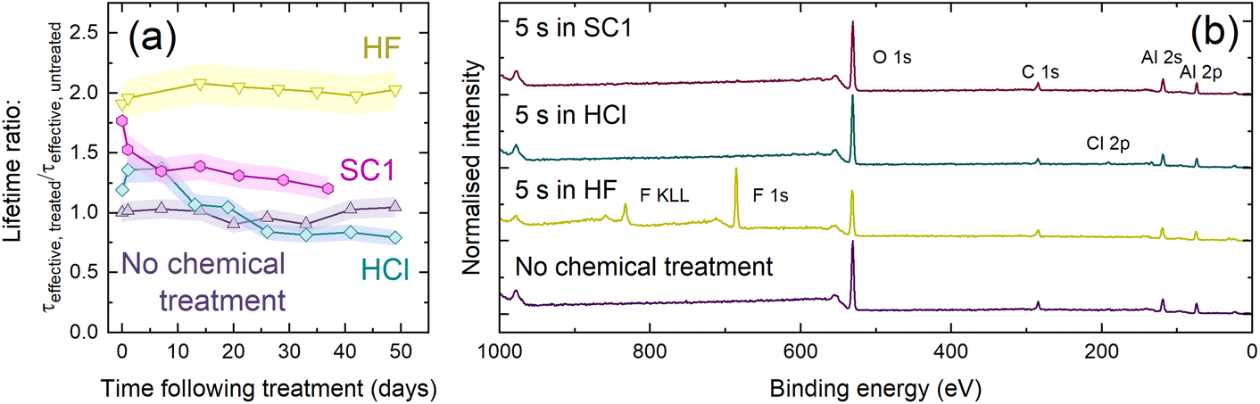 | ||
| Fig. 6 (a) Effective lifetime enhancement (defined as τeffective, treated/τeffective, untreated at Δn = 1 × 1015 cm−3) as a function of time exposed to ambient conditions following chemical (HF/HCl/SC1) treatment, with an untreated control. Each point was the average of five measurements and has an assumed uncertainty of ±8%.32 Connections between data points serve as a guide to the eye. (b) XPS survey scans of Si/HfO2/Al2O3 with no chemical treatment (purple) and following 5 s in 1% HF (yellow), 1% HCl (blue) or SC1 (purple), with regions corresponding to key XPS core levels identified. | ||
The samples were also characterised with XPS, with survey scans shown in Fig. 6(b). XPS analysis highlights a difference in the substrate surface resulting from each chemical treatment. Although prominent F 1s and F KLL signals were seen following HF treatment, only a very weak Cl 2p peak was seen at ∼200 eV following 5 s immersion in HCl.57 This peak suggests some surface residue may remain following HCl immersion, similar to that seen following HF immersion. No such residue is detected following SC1 immersion, as evidenced by the lack of a N 1s signal at ∼400 eV.57
Experimental
Sample preparation
13) were deposited onto silicon from a nominally identical batch, excepting a reduced thickness of ∼125 μm. For experiments on p-type silicon, Ga-doped, high quality, ∼150 μm thick, (100) orientation, 5 Ω cm, chemically etched p-type Czochralski-grown silicon wafers were used.
Samples were prepared following a previously reported chemical cleaning and etching procedure.71 The final step in the cleaning process (immersion in 2% HF for 60 s) was modified to immersion in 1% HF/1% HCl for 5 min with no subsequent water rinse, as this has been found to improve final passivation quality.17 Coatings were grown via plasma-enhanced ALD using a Veeco Fiji G2 system with an external load lock. Films were deposited on both sides of each wafer at 200 °C using O2 plasma, from trimethylaluminum (for Al2O3) and tetrakis(dimethylamido)hafnium (for HfO2) precursors. Growth rates are reported by the supplier to be ∼1.3 Å cycle-1 (Al2O3) and ∼1 Å cycle-1 (HfO2). A post-deposition anneal in air was performed for 30 min in a quartz tube furnace at temperatures between 350–600 °C.
:1:1 ratio). H2O2 (30–31% in water) was obtained from Technic Inc., NH4OH (28–30% in water) from CMC Materials, HCl (37%) from BASF, and HF (48.5–50% in water) from Sigma-Aldrich. Samples were immersed for 5 s intervals, and blow dried with N2 following immersion, prior to undergoing characterisation. Fresh solutions were used for the chemical treatment steps, reducing the likelihood of any contamination from prior cleaning processes.
HF safety considerations
Dilute HF is used in this work as a means to enhance passivation quality. It is important to note that HF is extremely corrosive and toxic,72 and must be handled only by those trained in HF handling, its hazards, and response in the event of exposure or spills. Exposure to HF and its fumes, even small quantities, can be fatal, and HF work should be conducted in a well-ventilated fume hood with appropriate personal protective equipment: face shield, apron, and HF-resistant gloves. HF etches glass, so HF work must be carried out in beakers compatible with HF.Characterisation
Passivation quality was quantified in terms of SRV defined by eqn (1) with τbulk taken as the intrinsic (i.e., radiative and Auger) limit using the parametrization of Niewelt et al.,31 taking photon recycling into account by assuming planar sample surfaces. For SRV extraction, we assume a constant τbulk as prior work using nominally identical Si substrates coated with HfO2 found no change or degradation in bulk lifetime at the annealing temperatures used herein.30 Assuming no extrinsic contribution to τbulk means values of SRV are upper limits. J0,s values, which have a relative uncertainty estimated to 10%,74 were determined via an automated fit by the Sinton Lifetime Tester software (v.5.74) using a 2-point method without smoothing around Δn = 1 × 1015 cm−3. A discussion on extracting J0,s from this region can be found in ref. 18. Our samples are generally coated with identical dielectric films on both sides, hence we state single-side J0,s values by dividing the extracted J0,s by 2.75
Conclusions
We have shown that Si surface passivation using HfO2 films can be improved with a two-step process: (1) the application of an Al2O3 capping layer; and (2) immersion in dilute HF. Employing both steps ultimately achieves SRVs < 2 cm s−1. Stacks of Si/HfO2/Al2O3 with 1 nm HfO2 treated with HF are stable for 50 days with thermal stability up to 450 °C.The results presented in this work suggest the enhancement achieved is related to changes at the dielectric surface. XPS analysis showed direct evidence of fluorination of the dielectric layers following HF immersion, and this correlates with the effective lifetime and KP measurements, suggesting the enhancement may result from formation of surface charges. Nevertheless, we cannot rule out the role of hydrogen and its ability to passivate the silicon–dielectric interface. Thus, an alternative enhancement mechanism could arise due to dissociation of HF at the dielectric surface, subsequently enabling fluorination of the dielectric film (either HfO2 or Al2O3) and thus freeing up H+ to interact with and passivate interface defects (as for the alneal process27,46). Direct detection of atomic hydrogen is experimentally very challenging. The observed fluorination could be indicative of hydrogenation, however this does not explain the enhancements observed when immersed in fluorine-free solutions (HCl- and NH4OH-based solutions).
When the dielectric stack is reversed (i.e., HfO2 is the capping layer, rather than Al2O3) we observe neither a passivation enhancement nor any evidence of halogenation through XPS analysis. Similarly, when individual layers are chemically treated, we observe that the passivation level does not change. This work therefore demonstrates that when Al2O3 is deposited on top of (thin or thick) HfO2, subsequent thinning down of the Al2O3 film substantially enhances the HfO2 passivation, with attained SRVs and J0,s values being competitive with current passivating contacts, interlayers, and capping layer passivation schemes.
Author contributions
The research concept was devised by S.L.P., N.E.G., and J.D.M. Experimental work, sample processing, characterization, and data analysis were largely conducted by S.L.P. XPS data were collected and analysed by E.K. with assistance from M.W. N.E.G. developed the corona charging methodology. A.W. contributed to the development of HfO2 passivation and temporal stability measurements. S.L.P., E.K., T.N., N.E.G., and J.D.M. contributed to discussions and data analysis. The manuscript was written by S.L.P. and J.D.M., with input from T.N., E.K and N.E.G.Data availability
Data underpinning figures in this paper can be freely downloaded from https://wrap.warwick.ac.uk/176204/. Requests for additional data should be made directly to the corresponding authors.Conflicts of interest
There are no conflicts to declare.Acknowledgements
S. L. P. and A. W. acknowledge funding from the Engineering and Physical Sciences Research Council (EPSRC) Doctoral Training Partnership (EP/R513374/1). Work was supported by the EPSRC Charged Oxide Inversion Layer (COIL) solar cells project (EP/V037749/1), and the Leverhulme Trust (RPG-2020-377). M. W. acknowledges financial support from the EPSRC-funded Warwick Analytical Science Centre (EP/V007688/1).References
- M. Fischer, M. Woodhouse, S. Herritsch and J. Trube, International Technology Roadmap for Photovoltaic (ITRPV): 2021 Results, VDMA, Frankfurt, Germany, 2022 Search PubMed.
- L. E. Black, in New perspectives on surface passivation: Understanding the Si-Al2O3 interface, Springer, 2016, ch. 2.6, p. 27 Search PubMed.
- T. G. Allen, J. Bullock, X. Yang, A. Javey and S. de Wolf, Nat. Energy, 2019, 4, 914–928 CrossRef CAS.
- B. Santos, Longi claims world's highest efficiency for p-type, indium-free HJT solar cells, https://www.pv-magazine.com/2022/12/22/longi-claims-worlds-highest-efficiency-for-p-type-indium-free-hjt-solar-cells/, (accessed 16 March, 2023).
- F. Feldmann, M. Simon, M. Bivour, C. Reichel, M. Hermle and S. W. Glunz, Appl. Phys. Lett., 2014, 104, 181105 CrossRef.
- F. Feldmann, M. Bivour, C. Reichel, H. Steinkemper, M. Hermle and S. W. Glunz, Sol. Energy Mater. Sol. Cells, 2014, 131, 46–50 CrossRef CAS.
- R. S. Bonilla, B. Hoex, P. Hamer and P. R. Wilshaw, Phys. Status Solidi A, 2017, 214, 1700293 CrossRef.
- H. B. Profijit, S. E. Potts, M. C. M. van de Sanden and W. M. M. Kessels, J. Vac. Sci. Technol., A, 2011, 29, 050801 CrossRef.
- P. Repo, A. Haarahiltunen, L. Sainiemi, M. Yli-Koski, H. Talvitie, M. C. Schubert and H. Savin, IEEE J. Photovolt., 2013, 3, 90–94 Search PubMed.
- C. Ballif, F.-J. Haug, M. Boccard, P. J. Verlinden and G. Hahn, Nat. Rev. Mater., 2022, 7, 597–615 CrossRef.
- B. Hoex, S. B. B. Heil, E. Langereis, M. C. M. van de Sanden and W. M. M. Kessels, Appl. Phys. Lett., 2006, 89, 042112 CrossRef.
- G. Dingemans and W. M. M. Kessels, J. Vac. Sci. Technol., A, 2012, 30, 040802 CrossRef.
- S. L. Pain, E. Khorani, T. Niewelt, A. Wratten, G. J. P. Fajardo, B. Winfield, R. S. Bonilla, M. Walker, L. F. J. Piper, N. E. Grant and J. D. Murphy, Adv. Mater. Interfaces, 2022, 9, 2201339 CrossRef CAS.
- X. Cheng, P. Repo, H. Halvard, A. P. Perros, E. S. Marstein, M. Di Sabatino and H. Savin, IEEE J. Photovolt., 2017, 7, 479–486 Search PubMed.
- F. Lin, B. Hoex, Y. H. Koh, J. Lin and A. G. Aberle, Energy Procedia, 2012, 15, 84–90 CrossRef CAS.
- A. B. Gougam, B. Rajab and A. B. Afif, Mater. Sci. Semicond. Process., 2019, 95, 42–47 CrossRef CAS.
- N. E. Grant, A. I. Pointon, R. Jefferies, D. Hiller, Y. Han, R. Beanland, M. Walker and J. D. Murphy, Nanoscale, 2020, 12, 17332–17341 RSC.
- B. Hammann, B. Steinhauser, A. Fell, R. Post, T. Niewelt, W. Kwapil, A. Wolf, A. Richter, H. Höffler and M. C. Schubert, IEEE J. Photovolt., 2023 DOI:10.1109/JPHOTOV.2023.3265859.
- G. Dingemans, M. M. Mandoc, S. Bordihn, M. C. M. van de Sanden and W. M. M. Kessels, Appl. Phys. Lett., 2011, 98, 222102 Search PubMed.
- N. E. Grant, T. C. Kho and K. Weber, IEEE J. Photovolt., 2015, 5, 1047–1052 Search PubMed.
- G. Dingemans, P. Engelhart, R. Seguin, F. Einsele, B. Hoex, M. C. M. van de Sanden and W. M. M. Kessels, J. Appl. Phys., 2009, 106, 114907 CrossRef.
- F. Kersten, R. Lantzsch, N. Buschmann, Y. Neumann, K. Petter, M. Kauert, F. Stenzel, F. Fertig, A. Schönmann, B. Faulwetter-Quandt, K. Duncker, K. Kim, E. Jarzembowski, M. Junghänel, A. Weihrauch, S. Wasmer, B. Reiche, C. Klenke, B. Lee, F. Frühauf, I. Höger, M. Schaper, J. W. Müller and D. J. W. Jeong, AIP Conf. Proc., 2022, 2487, 130007 CrossRef CAS.
- G. Dingemans, M. C. M. van de Sanden and W. M. M. Kessels, Phys. Status Solidi RRL, 2011, 5, 22–24 CrossRef CAS.
- B. W. H. van de Loo, B. Macco, J. Melskens, W. Beyer and W. M. M. Kessels, J. Appl. Phys., 2019, 125, 105305 CrossRef.
- D. K. Simon, P. M. Jordan, T. Mikolajick and I. Dirnstorfer, ACS Appl. Mater. Interfaces, 2015, 7, 28215–28222 CrossRef CAS PubMed.
- J. Panigrahi, Vandana, R. Siingh and P. K. Singh, Sol. Energy Mater. Sol. Cells, 2018, 188, 219–227 CrossRef CAS.
- G. Dingemans, F. Einsele, W. Beyer, M. C. M. van de Sanden and W. M. M. Kessels, J. Appl. Phys., 2012, 111, 093713 CrossRef.
- J.-I. Polzin, B. Hammann, T. Niewelt, W. Kwapil, M. Hermle and F. Feldmann, Sol. Energy Mater. Sol. Cells, 2021, 230, 111267 CrossRef CAS.
- N. E. Grant, S. L. Pain, J. T. White, M. Walker, I. Prokes and J. D. Murphy, ACS Appl. Energy Mater., 2022, 5, 1542–1550 CrossRef CAS.
- A. Wratten, S. L. Pain, D. Walker, A. B. Renz, E. Khorani, N. E. Grant and J. D. Murphy, IEEE J. Photovolt., 2023, 13, 40–47 Search PubMed.
- T. Niewelt, B. Steinhauser, A. Richter, B. Veith-Wolf, A. Fell, B. Hammann, N. E. Grant, L. Black, J. Tan, A. Youssef, J. D. Murphy, J. Schmidt, M. C. Schubert and S. W. Glunz, Sol. Energy Mater. Sol. Cells, 2022, 235, 111467 CrossRef CAS.
- A. L. Blum, J. S. Swirhun, R. A. Sinton, F. Yan, S. Herasimenka, T. Roth, K. Lauer, J. Haunschild, B. Lim, K. Bothe, Z. Hameiri, B. Seipel, R. Xiong, M. Dhamrin and J. D. Murphy, IEEE J. Photovolt., 2014, 4, 525–531 Search PubMed.
- B. W. H. van de Loo, B. Macco, M. Schnabel, M. K. Stodolny, A. A. Mewe, D. L. Young, W. Nemeth, P. Stradins and W. M. M. Kessels, Sol. Energy Mater. Sol. Cells, 2020, 215, 110592 CrossRef CAS.
- Z. Zhang, Y. Zeng, Y. Huang, X. Guo, Z. Wang, Q. Yang, C. Shou, B. Yan and J. Ye, presented in part at the IEEE 46th Photovoltaic Specialists Conference (PVSC), Chicago, USA, 2019.
- E. Oudot, M. Gros-Jean, K. Courouble, F. Bertin, R. Duru, N. Rochat and C. Vallee, J. Vac. Sci. Technol., A, 2018, 36, 01A116 CrossRef.
- T. N. Truong, D. Yan, W. Chen, M. Tebyetekerwa, M. Young, M. Al-Jassim, A. Cuevas, D. Macdonald and H. T. Nguyen, Sol. RRL, 2020, 4, 1900476 CrossRef CAS.
- R. L. Opila, D. Yang, N. Kotulak, L. Costello and B. Chhabra, 38th IEEE Photovoltaic Specialists Conference, 2012.
- A. I. Pointon, N. E. Grant, E. C. Wheeler-Jones, P. P. Altermatt and J. D. Murphy, Sol. Energy Mater. Sol. Cells, 2018, 183, 164–172 CrossRef CAS.
- S. Jafari, U. Varshney, B. Hoex, S. Meyer and D. Lausch, IEEE J. Photovolt., 2021, 11, 1361–1369 Search PubMed.
- H. Huang, J. Lv, Y. Bao, R. Xuan, S. Sun, S. Sneck, S. Li, C. Modanese, H. Savin, A. Wang and J. Zhao, Sol. Energy Mater. Sol. Cells, 2017, 161, 14–30 CrossRef CAS.
- Z. Yang, J. Krugener, F. Feldmann, J.-I. Polzin, B. Steinhauser, T. T. Le, D. Macdonald and A. Liu, Adv. Energy Mater., 2022, 12, 2103773 CrossRef CAS.
- A. Liu, Z. Yang, F. Feldmann, J.-I. Polzin, B. Steinhauser, S. P. Phang and D. Macdonald, Sol. Energy Mater. Sol. Cells, 2021, 230, 111254 CrossRef CAS.
- D. Hiller, P. Hönicke and D. König, Sol. Energy Mater. Sol. Cells, 2020, 215, 110654 CrossRef CAS.
- R. S. Bonilla, N. Jennison, D. Clayton-Warwick, K. A. Collett, L. Rangs and P. R. Wilshaw, Energy Procedia, 2016, 92, 326–335 CrossRef CAS.
- J. Zhao, A. Wang, P. P. Altermatt, S. R. Wenham and M. A. Green, Sol. Energy Mater. Sol. Cells, 1996, 41–42, 87–99 CrossRef.
- M. J. Kerr and A. Cuevas, Semicond. Sci. Technol., 2002, 17, 35–38 CrossRef CAS.
- R. S. Bonilla, Mater. Res. Express, 2022, 9, 085901 CrossRef.
- L. Kronik and Y. Shapira, Surf. Sci. Rep., 1999, 37, 1–206 CrossRef CAS.
- V. Aubriet, K. Courouble, M. Gros-Jean and Ł. Borowik, Rev. Sci. Instrum., 2021, 92, 083905 CrossRef CAS PubMed.
- R. J. Hamers and K. Markert, Phys. Rev. Lett., 1990, 64, 1051–1054 CrossRef CAS PubMed.
- A. Henning, G. Günzburger, R. Jöhr, Y. Rosenwaks, B. Bozic-Weber, C. E. Housecroft, E. C. Constable, E. Meyer and T. Glatzel, Beilstein J. Nanotechnol., 2013, 4, 416–428 Search PubMed.
- M. Chen, J. H. Hack, X. Lin, A. Janotti and R. L. Opila, Coatings, 2018, 8, 108 CrossRef.
- X. Yang, Z. Ying, Z. Yang, J.-R. Xu, W. Wang, J. Wang, Z. Wang, L. Yao, B. Yan and J. Ye, Adv. Sci., 2021, 8, 2003245 CrossRef CAS PubMed.
- S. W. Glunz, D. Biro, S. Rein and W. Warta, J. Appl. Phys., 1999, 86, 683–691 CrossRef CAS.
- R. S. Bonilla, C. Reichel, M. Hermle, P. Hamer and P. R. Wilshaw, Appl. Surf. Sci., 2017, 412, 657–667 CrossRef CAS.
- J. Panigrahi, Vandana, R. Singh, C. M. S. Rauthan and P. K. Singh, AIP Adv., 2017, 7, 035219 CrossRef.
- National Institute of Standards and Technology, NIST X-ray Photoelectron Spectroscopy Database, 20, National Institute of Standards and Technology, Maryland, USA, 4.1 edn, 2000.
- T. P. Smirnova, L. V. Yakovkina, V. N. Kitchai, V. V. Kaichev, Y. V. Shubin, N. B. Morozova and K. V. Zherikova, J. Phys. Chem. Solids, 2008, 69, 685–687 CrossRef CAS.
- S. Tougaard, QUASES-IMFP-TPP2MM (Revision 3.0), 2016.
- S. Tanuma, C. J. Powell and D. R. Penn, Surf. Interface Anal., 1994, 21, 165–176 CrossRef CAS.
- G. Masmitjà, P. Ortega, I. Martín, J. Pérez, G. López, E. Calle, L. G. Gerling, C. Voz and R. Alcubilla, Barcelona, Spain, 2017.
- Q. Cheng, M. K. Benipal, Q. Liu, X. Wang, P. A. Crozier, C. K. Chan and R. J. Nemanich, ACS Appl. Mater. Interfaces, 2017, 9, 16138–16147 CrossRef CAS PubMed.
- T. L. Barr, Appl. Surf. Sci., 1982, 15, 1–35 Search PubMed.
- P. Castrucci, M. Scarselli, M. D. Crescenzi, M. Diociaiuti, P. S. Chaudhari, C. Balasubramanian, T. M. Bhave and S. V. Bhoraskar, Thin Solid Films, 2006, 508, 226–230 CrossRef CAS.
- M. Balsubramanian, L. K. Bera, S. Mathew, N. Balasubramanian, V. Lim, M. S. Joo and B. J. Cho, Thin Solid Films, 2004, 462–463, 101–105 CrossRef.
- D. Triyoso, R. Liu, D. R. M. Ramon, N. V. Edwards, R. Gregory, D. Werho, J. Kulik, G. Tam, E. Irwin, X.-D. Wang, L. B. La, C. Hobbs, R. Garcia, J. Baker, B. E. White, Jr. and T. Tobin, J. Electrochem. Soc., 2004, 151, F220–F227 CrossRef CAS.
- J. Melskens, B. W. H. van de Loo, B. Macco, L. E. Black, S. Smit and W. M. M. Kessels, IEEE J. Photovolt., 2018, 8, 373–388 Search PubMed.
- F. Feldmann, G. Nogay, J.-I. Polzin, B. Steinhauser, A. Richter, A. Fell, C. Schmiga, M. Hermle and S. W. Glunz, IEEE J. Photovolt., 2018, 8, 1503–1509 Search PubMed.
- C. Reichel, F. Feldmann, A. Richter, J. Benick, M. Hermle and S. W. Glunz, Prog. Photovolt.: Res. Appl., 2022, 30, 288–299 CrossRef CAS.
- W. Kern, J. Electrochem. Soc., 1990, 137, 1887–1892 CrossRef CAS.
- N. E. Grant, P. P. Altermatt, T. Niewelt, R. Post, W. Kwapil, M. C. Schubert and J. D. Murphy, Sol. RRL, 2021, 5, 2000754 CrossRef CAS.
- Sigma Aldrich, MSDS – 339261, https://www.sigmaaldrich.com/GB/en/sds/sigald/<?ccdc_no 339261?>339261<?ccdc END?>, (accessed 21st March, 2023).
- M. Kessler, T. Ohrdes, P. P. Altermatt and R. Brendel, J. Appl. Phys., 2012, 111, 054508 CrossRef.
- D. E. Kane and R. M. Swanson, presented in part at the 18th IEEE Photovoltaic Specialists Conference, Las Vegas, 1985.
- D. Kang, H. C. Sio, J. Stuckelberger, D. Yan, S. P. Phang, R. Liu, T. N. Truong, T. Le, H. T. Nguyen, X. Zhang and D. Macdonald, Prog. Photovolt.: Res. Appl., 2022, 30, 970–980 CrossRef CAS.
- I. D. Baikie, S. Mackenzie, P. J. Z. Estrup and J. A. Meyer, Rev. Sci. Instrum., 1991, 62, 1326–1332 CrossRef CAS.
- B. Hoex, J. Schmidt, M. C. M. van de Sanden and W. M. M. Kessels, presented in part at the 33rd IEEE Photovoltaic Specialist Conference (PVSEC 2008), California, USA, 2008.
- L. G. A. Melo, A. P. Hitchcock, D. Susac, J. Stumper and V. Berejnov, Phys. Chem. Chem. Phys., 2018, 20, 16625–16640 RSC.
Footnote |
| † Electronic supplementary information (ESI) available: Experimental results for experiments on p-type samples, details and results of control experiments and additional Kelvin probe data. See DOI: https://doi.org/10.1039/d3nr01374j |
| This journal is © The Royal Society of Chemistry 2023 |