A layer-stacked NiO nanowire/nanosheet homostructure for electrochromic smart windows with ultra-large optical modulation

Yi Gao , Pengyang Lei , Siyu Zhang , Huanhuan Liu , Chengyu Hu , Zhu Kou , Jinhui Wang * and Guofa Cai *
Key Laboratory for Special Functional Materials of Ministry of Education, National & Local Joint Engineering Research Center for High-efficiency Display and Lighting Technology, School of Materials and Engineering, and Collaborative Innovation Center of Nano Functional Materials and Applications, Henan University, Kaifeng 475004, China. E-mail: jinhui.wang@henu.edu.cn; caiguofa@henu.edu.cn

Received 16th March 2023 , Accepted 14th April 2023

First published on 14th April 2023


Abstract

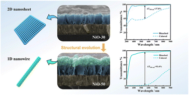
The structural engineering of active materials at the nanoscale level is crucial to improving the performance of electrochromic devices. However, an insufficient structural design inevitably results in limited electron/ion transportation and inadequate electrochromic performance. Herein, a new type of layer-stacked nanowire/nanosheet homostructure is proposed for enhancing the electrochromic properties of transition metal oxide films. Benefiting from the one-pot feature integration of nanowire and nanosheet structures, the NiO film with a unique homostructure delivers ultra-large optical modulation up to 93.4% at 550 nm and a high coloration efficiency of 72.1 cm2 C−1 in comparison with NiO-based materials. In addition, the film maintains 91% of its optical modulation over 1000 cycles of coloration and bleaching processes. Furthermore, the high performance of the device was verified by integrating the NiO film with the TiO2 ion storage layer in assembled smart windows with a dual function of electrochromic and energy storage. As a proof of concept, the integration of solar cells with electrochromic devices demonstrates the great significance of self-powered smart windows for energy-saving. To this end, such a strategy of structural design for electrochromic films would offer a distinctive pathway toward studying high-performance electrochromic systems.


Introduction

Electrochromism is rapidly developed concerning implementation in smart windows, electronic displays, switchable glasses, and rearview mirrors.1–4 As an example, the electrochromic smart window can manage light and heat radiation by controlling its optical properties, thus efficiently increasing living comfort and reducing energy consumption in modern buildings.5–7 It should be noted that the design and fabrication of high-performance electrochromic materials are crucial for promoting the practical application of smart windows.8,9 In particular, the ultra-large optical modulation and neutral opaque color in the electrochromic materials are extraordinarily desirable for smart windows due to their role in protecting personal privacy and avoiding light pollution in buildings to the greatest extent.

As an anode electrochromic material, nickel oxide (NiO) possesses a transmissive-to-black color tunability, a wide range of visible light modulation and good photothermal stability.8–10 Nevertheless, it is still a significant challenge for NiO films to achieve stable ultra-large optical modulation, which is also an issue faced by other transition metal oxides. In recent years, great efforts have been put into designing a variety of micro-/nano-structures with various dimensionalities, including nanoparticle-, nanosheet-, and dandelion flower-type NiO films.11–15 However, the singleness of the reported NiO nanostructures show that their bleaching and coloration states in electrochromism cannot be synchronously optimized, which results in difficult breakthroughs in satisfactory optical modulation. Additionally, the excessive stress generated in the electrochromic process also causes cycling instability for a single NiO structure. In this regard, it is of great importance to establish a smart strategy of structural design, wherein ultra-large optical modulation is guaranteed without sacrificing cycling stability.

In the wide variety of structures of transition metal oxides, nanowire networks with high porosity and high aspect ratios can provide efficient channels for electrolyte ion diffusion.16–18 Therefore, the nanowire structure in electrochromism is speculated to have the capability of efficient coloration. On the other hand, the nanosheets are usually formed with an ordered vertical structure on the substrate, which has better structural stability and a larger contact area with the substrate.19,20 These features of the nanosheet structure can improve the electron transfer kinetics and electrochemical conductivity of electrochromic materials with good cycling stability.21 Importantly, the porous properties of nanosheet structures have a large difference from those of nanowire structures. To this end, we envisage that integrating nanowire and nanosheet structures with independent optoelectronic properties into a single hierarchical homostructure can provide sufficient tunability for the electrochromic properties.

In this study, we present a novel layer-stacked transmissive-to-black NiO film with a nanowire/nanosheet homostructure by a facile hydrothermal method. This unique structure can provide the following merits: first, one-pot construction of a nanowire/nanosheet homostructure ensuring uninterrupted electron transport and convenient ion diffusion, greatly enhancing its electrochromic properties, and second, the optical modulation of the NiO film which can be effectively tuned by controlling the nanowire-layer thickness. As a result, compared with NiO-based electrochromic materials, our layer-stacked homostructure provides a high coloration efficiency of 72.1 cm2 C−1, a good cycling stability of 91% over 1000 cycles, and an ultra-large optical modulation range of up to 93.4%. Furthermore, we developed a photovoltaic electrochromic smart window composed of NiO electrodes and TiO2 counter electrodes to realize the self-powering of smart windows under ambient solar radiation. Smart windows can dynamically adjust the visible sunlight and efficiently store electrical energy to achieve the goal of energy-saving.

Experimental

Materials

All chemical reagents, namely, nickel(II) chloride hexahydrate (NiCl2·6H2O), urea (CH4N2O), titanium tetrachloride (TiCl4), hydrogen peroxide (H2O2), potassium hydroxide (KOH), polyvinyl alcohol (PVA, 89[thin space (1/6-em)]000–98[thin space (1/6-em)]000, 99+% hydrolyzed), ammonium hydroxide, acetone, and ethanol, used in the experiment were purchased from Sigma-Aldrich. All reagents were of analytical grade and used without further purification. Fluorine-doped tin oxide (FTO)-coated transparent conductive glass (sheet resistance: ∼14 Ω, thickness: ∼2.2 mm) was purchased from Zhuhai Kaivo Electronic Components Co., Ltd.

Preparation of NiO films

The NiO films were synthesized by a hydrothermal method. The hydrothermal precursor solution was obtained by dissolving 0.237 g NiCl2·6H2O and 0.06 g urea in 20 mL deionized water under stirring for 10 min at room temperature. Afterward, the autoclave (50 mL) with the precursor solution was sealed and maintained at 140 °C for different times (30 min, 35 min, 50 min, 70 min, 90 min, and 110 min), in which the conductive surface of FTO faced downwards. Then, a light green film was grown on the FTO substrate (Fig. S1), followed by rinsing with deionized water (18.25 MΩ cm) and drying at 60 °C for 3 h. Finally, NiO films with light brown in colour were fabricated after the annealing process at 300 °C for 2 h.

Preparation of TiO2 films

The TiO2 precursor sol was first prepared by a previously reported sol–gel method.22 Then, the precursor sol was transformed into white suspension by hydrothermal treatment at 150 °C for 12 h. TiO2 thin films were further prepared by the electrostatic spray deposition (ESD) method. 1 mg mL−1 of ink was then prepared by mixing 2 mL of the hydrothermal suspension with 10 mL of deionized water and ethanol (v[thin space (1/6-em)]:[thin space (1/6-em)]v, 1[thin space (1/6-em)]:[thin space (1/6-em)]1), and a DC voltage of 19 kV was applied to drive the ink in the metal needles to be sprayed to the FTO substrate at a flow rate of 0.6 mL h−1. Finally, TiO2 films were successfully prepared.

Fabrication of the gel electrolyte

The electrolyte was prepared as follows: 3 g of PVA was dissolved in 30 mL of deionized water at 85 °C in an oil bath under stirring. Then, 0.2244 g of KOH was dissolved in 10 mL of deionized water and the dissolved KOH solution was dripped into the cooled PVA solution to form the 0.1 M KOH/PVA gel electrolyte. Finally, the semi-solid electrolyte was obtained.

Assembly of the electrochromic device

First, the obtained NiO film and TiO2 film were used as the electrochromic electrode and the ion storage electrode, respectively. The 0.1 M KOH/PVA gel electrolyte was slowly injected in between two electrodes, in which the space was created with VHB transparent mounting tape (3 M, 4010) with a thickness of 1 mm. By subsequent encapsulation with epoxy resin adhesive, the electrochromic device was finally fabricated.

Materials characterization

The crystal structure and phase composition of Ni(OH)2 and NiO were characterized by X-ray diffraction (XRD, D8-ADVANCE). The morphology of the sample was analyzed using a field emission scanning electron microscope (SEM, Navo NanoSEM 450). The transmission electron microscope (TEM, JEM-2100) was used to further study the morphology and crystal structure of the sample. X-ray photoelectron spectroscopy (XPS, AXIS ULTRA) was used to determine the element valence states of the sample. Fourier transform infrared spectroscopy (FTIR, FIR STA 8000) is used to demonstrate the structure and chemical bonds of molecules.

Electrochromic and electrochemical characterizations

By combining an electrochemical workstation (PGSTAT302N, Switzerland) with an ultraviolet-visible-near-infrared (UV-Vis-NIR) spectrophotometer (Shimadzu UV-3600 plus, Japan), the electrochemical and photoelectric performances of the samples were in situ synchronously measured. The NiO electrochromic film, Pt foil, and Ag wire were used as a working electrode, a counter electrode, and a reference electrode, respectively. Cyclic voltammetry (CV), square wave potential, and galvanostatic charge–discharge measurements were performed on the electrochemical workstation. The in situ electrochromic properties of the samples in response to different electrochemical stimulation conditions were measured using a UV-Vis-NIR spectrophotometer.

Results and discussion

To begin with, Ni(OH)2 films were in situ grown on FTO glass substrates at 140 °C with the structure-directing urea (Fig. S1). The annealing process for samples at 300 °C was then carried out to facilitate the material transformation from Ni(OH)2 to NiO. In order to examine the relationship between electrochromic properties and structural evolution, a series of NiO films with different hydrothermal reaction times (30 min, 35 min, 50 min, 70 min, 90 min, and 110 min) are labeled as NiO-30, NiO-35, NiO-50, NiO-70, NiO-90, and NiO-110, respectively. The XRD pattern shows diffraction peaks at 2θ degrees of 36.9°, 43.3°, and 62.9°, which can be assigned to (111), (200), and (220) reflections of the cubic NiO phase (JCPDS 00-047-1049), verifying the successful formation of the NiO film (Fig. S2).23–25 The chemical composition and valence state of NiO films were further analyzed using X-ray photoelectron spectroscopy (XPS, Fig. S3). The survey spectrum indicates the presence of Ni, O, and C elements. The Ni 2p spectrum contains two peaks of Ni2+ (853.9 and 871.8 eV) and Ni3+ (855.7 and 873.2 eV) accompanied by two satellite peaks (861.4 and 879.5 eV). The O 1s spectrum reflects the oxygen-containing bond in the NiO film. By fitting the spectrum, the oxygen-containing bond can be divided into three types of oxygen (O1, O2, and O3), which are typical Ni–oxygen bonds (at 529.7 eV), oxygen generated at the oxygen defect site (at 531.2 eV), and oxygen related to water adsorption on the surface of electrodes (at 531.7 eV), respectively. These results further demonstrate our successful preparation of NiO films.20,26–28

The structural evolution of the NiO film was characterized by scanning electron microscopy (SEM). When the hydrothermal time is controlled at 30 min, the nanosheet-type NiO layer with a thickness of ∼400 nm was in situ grown on the FTO substrate (Fig. 1a and b). The porous size between nanosheets with 40–300 nm contributes to the ion transport and optically transparent state of the NiO film in electrochromism. Interestingly, it was found that further hydrothermal reaction leads to the structural evolution from a nanosheet to a nanowire (Fig. 1d and Fig. S4). The cross-section analysis verifies that the interspace of intertwined and disordered nanowire networks was formed on the top of the nanosheet layer (Fig. 1e and Fig. S5). The thickness of nanosheet layers for NiO-50 and NiO-110 is almost equal to that of NiO-30, demonstrating the independent growth of nanowires without sacrificing the nanosheet structure. Layer-stacked NiO films can be one-pot constructed in this hydrothermal system. In addition, the structures of NiO-30 and NiO-50 films were further verified by transmission electron microscopy (TEM) characterization (Fig. 1c and f, Fig. S6). Both nanowires and nanosheets have interplanar spacings of 0.24 and 0.21 nm which coincide with the results of our XRD analysis.


image file: d3nr01211e-f1.tif
Fig. 1 Morphology characterization of the NiO-30 film with a nanosheet structure: (a) SEM image, (b) cross-section pattern, and (c) TEM images; morphology characterization of a layer-stacked NiO-50 film with nanosheet and nanowire structures: (d) SEM image, (e) cross-section pattern, and (f) TEM images.

The formation process of the NiO homostructure with nanosheets and nanowires is represented by schematic diagrams (Fig. 2a). CO32− and OH anions generated by urea hydrolysis play an important role in the structural evolution of films at different stages of hydrothermal reaction. Due to the smaller solubility product Ksp of OH than that of CO32−, the OH has relatively high supersaturation (S) and was dominant in the short-term reaction, which can be reflected by the pH values of the precursor solution in the first 30 minutes of the reaction process. According to the Thomson–Gibbs equation, a high S solution generally induces high chemical potential and surface energy of the growing crystal, resulting in a high nucleation rate and further the formation of a two-dimensional (2D) nanosheet structure.29 Fourier transform infrared spectroscopy (FTIR) analysis in Fig. 2b shows that the nanosheet-type sample exhibits a single characteristic peak at 647 cm−1 corresponding to the bending vibration of the Ni–O–H group, demonstrating that the dominant OH easily leads to the precipitation of Ni(OH)2. In the long-term reaction process, it can be observed from FTIR results that new absorption peaks are present at 1385, 1600, and 2202 cm−1, which correspond to the vibration bands of CO32− and HCO3 anions, respectively.30 The reduced pH value of the precursor solution further verifies the presence of carbonate anions generated by urea hydrolysis (Fig. 2c). Although OH is still involved in the construction of nickel hydroxide frameworks, carbonate anions are concluded to dominate the formation of the one-dimensional (1D) nanowire structure, owing to the relatively low S in the reaction solution.


image file: d3nr01211e-f2.tif
Fig. 2 (a) Schematic diagram of the evolution mechanism of the NiO homostructure with nanosheets and nanowires; (b) FTIR spectra of NiO-30 and NiO-50 films before annealing; (c) pH change curve as a function of different hydrothermal times.

To evaluate the electrochromic performance of NiO films, we first conducted cyclic voltammetry (CV) measurement of NiO-30 and NiO-50 films in a 1 M KOH electrolyte under a scan rate of 10 mV s−1 (Fig. 3a). The CV curves show that the potential window of a reversible redox reaction is limited between 0 V (vs. Ag wire) and 0.8 V (vs. Ag wire). In the forward scan, the NiO films undergo an oxidation reaction and coloration process. The OH ion intercalation causes the conversion of bleached NiO to colored NiOOH. In the negative scan, the reduction reaction of the film leads to the recovery of initial NiO and optical transmittance, revealing the excellent reversibility of the NiO film in the electrochromic process (Fig. S7). By comparison, the NiO-50 film exhibits significantly higher current densities than NiO-30, revealing that the grown nanowire network in the layer-stacked NiO-50 film has enhanced electrochemical activity and reaction kinetics.


image file: d3nr01211e-f3.tif
Fig. 3 Electrochromic and electrochemical performance of the NiO film in a 1 M KOH electrolyte. (a) Comparison of CV curves of NiO-30 and NiO-50 films at 550 nm at a scan rate of 10 mV s−1; (b) optical transmission spectra showing colored and bleached states of NiO-30 and NiO-50 films; (c) the corresponding in situ transmittance spectra of NiO-30 and NiO-50 films at square wave potentials of 0 V and 0.7 V (vs. Ag wire) for 40 s; (d) comparison of the electrochromic performance of different NiO films; (e) the variation of in situ optical density (ΔOD) and charge density; (f) cycling stability measurement of the NiO-50 film over 1000 cycles by applying alternating coloration and bleaching voltages for 100 s.

Optical modulation (ΔT) is a crucial parameter of electrochromic materials. It is defined as the difference in optical transmittance between bleached and colored states. It can directly reflect the capability of the electrochromic film to adjust thermal radiation and light intensity. Therefore, transmission spectra were recorded to compare the optical modulation of different NiO films in the wavelength range from 300 to 900 nm by applying a bleaching voltage of 0 V (vs. Ag wire) for 100 s and a coloration voltage of 0.7 V (vs. Ag wire) for 100 s with the FTO transmittance as the baseline (Fig. 3b and Fig. S8). It can be observed that the NiO-30 film with a nanosheet structure exhibits a small optical modulation of 37.8%. Nevertheless, the preliminary growth of nanowires in the NiO-35 film has a significant effect on its electrochromic performance, achieving an improved optical modulation of 83.1%. According to the calculated optical modulation per unit thickness (ΔTt), the ΔTt of the nanowire layer (0.214%) is twice as much as that of the nanosheet layer (0.095%), demonstrating our assumption that the nanowire structure with sufficient active sites has a larger contribution to the optical modulation than the nanosheet structure. With the further growth of nanowires, the NiO-50 film impressively achieves a wide range of ultra-large optical modulation of 93.4% at 550 nm and 63% at 800 nm in the visible and near-infrared regions. The bleached NiO-50 film can maintain transmittance as high as 95.9%. In the coloration state, the NiO-50 film presents a dark-brown neutral color with a transmittance of 2.5% approaching the limit (Fig. S9), which is beneficial for eye comfort and privacy protection. Nevertheless, the overgrowth of nanowires reversely causes a transmittance decrease from NiO-50 to NiO-110 films in the initial states, originating from the accumulation of their intrinsic color (Fig. S10).

Response time, as another important figure-of-merit for electrochromism, is defined as the time required for 90% of the total optical modulation.31,32 In this regard, the in situ dynamic transmission spectra of NiO films at 550 nm were measured by applying square wave potentials of 0.7 V (vs. Ag wire) and 0 V (vs. Ag wire) for 40 s. The coloration time tc and bleaching time tb of NiO-30 and NiO-50 films were calculated to be 4.3 s/3.4 s and 12.2 s/9.5 s, respectively (Fig. 3c). As summarized in Fig. 3d and Table S1, with the increase of nanowire thickness from NiO-30 to NiO-110 films, both tc and tb show an increasing trend at the beginning stage and decrease subsequently. The NiO-50 film especially presents the optimum optical modulation and moderate response time in comparison. Therefore, further study was carried out to explore the superiority of NiO-50 films in electrochromism.

Coloration efficiency (CE) can be defined as the change of the optical density (ΔOD) per unit charge (ΔQ) inserted into the electrochromic material. The CE of the NiO-50 film was calculated up to 72.1 cm2 C−1 at 550 nm according to the following formula: CE(λ) = ΔOD/ΔQ = log(Tb/Tc)/ΔQ. Tb and Tc represent the transmittance in the bleached and colored states. CE can be calculated by inserting a function of charge density in the linear region of the ΔOD diagram (Fig. 3e). It indicates that a small charge density of the inserted ion in the NiO-50 film can lead to the achievement of an optical modulation up to 93.4%, further proving the design rationality of the layer-stacked homostructure. The high CE also exhibits a direct correlation with the long-term working stability of electrochromic materials.33 Therefore, the cycling stability of the NiO-50 film was further measured by in situ recording of the transmittance at 550 nm under periodic coloration and bleaching potentials of 0.7 V (vs. Ag wire) and 0 V (vs. Ag wire) for 100 s (Fig. 3f and Fig. S11). Moreover, the insertion/extraction of ions is dominant in triggering the volume expansion of the electrode material, consistent with the reported nickel-based oxides with a large expansion coefficient in alkaline electrolytes.34 Despite this inevitable phenomenon, the NiO-50 film still maintains 91% over 1000 cycles, which can be attributed to the efficient inherent strain tolerance of the layer-stacked nanowire/nanosheet homostructure. As shown in the Nyquist plots (Fig. S12), it is observed that the NiO-50 film maintains low internal resistance (<16 Ω) in the high-frequency region before and after cycling, revealing its superior interface stability and efficient electron transport. Furthermore, the electrochromic properties of the NiO-50 film are compared with those of previously reported NiO materials fabricated by various methods (Table S2), revealing that the NiO-50 film exhibits much comparable coloration efficiency and cycling stability. Even though with moderate response time, this NiO film displays the highest optical modulation of 93.4%, which is also comparable to those of the other electrochromic materials, such as WO3, metals with reversible electrodeposition behavior.35,36 The optical memory property refers to the transmittance retention in bleached and colored states of electrochromic films under open-circuit conditions. Long-term stable retention signifies a low requirement for external power, which is of great significance to the energy-saving of smart windows. Therefore, after applying a potential of 0.7 V (vs. Ag wire) for coloration, the real-time memory record for the film under an open-circuit state shows that the optical transmittance is only attenuated by 36% after 24 h (Fig. S13), proving an excellent optical memory of the NiO-50 film.37,38

The integration of electrochromism with energy storage in one platform can allow the visualization of energy storage levels in real-time while enabling the recycling of supplied electricity to reduce energy consumption. Given the excellent electrochemical and electrochromic properties, the NiO-50 film is expected to possess high-performance energy storage capability. Therefore, galvanostatic charge–discharge (GCD) experiments were performed at different current densities, and their in situ spectra were simultaneously recorded. The corresponding areal capacities of the NiO-50 films were calculated to be 5.72 × 10⁻², 5.46 × 10⁻², 50 × 10−2, 3.99 × 10⁻² and 2.52 × 10⁻² mA h cm−2 (866.7, 827.2, 757.6, 604.5 and 381.8 mA h cm−3) at 0.1, 0.15, 0.2, 0.4, and 0.6 mA cm−2 (Fig. 4a), which are comparable to the previously reported NiO-based electrochromic energy storage materials.24,39,40 The highly symmetric charge–discharge curves show the high coulombic efficiency and electrochemical reversibility of the NiO-50 film. Furthermore, in situ transmission spectra at 550 nm were measured during the GCD measurement at current densities of 0.1 and 0.6 mA cm−2 to verify the visualization level of the NiO-50 film by color changes (Fig. 4b and c). At a low current density of 0.1 mA cm−2, the GCD process leads to the transmittance changes of the NiO-50 film from 86.9% to 4.9% and then reversibly back to 86.3%, while the color changed between transparent and brown-black. Charging and discharging under high current density generally cause inadequate redox reactions. Nevertheless, our results reveal that the NiO-50 film still can maintain 61% of reversible optical modulation under 0.6 mA cm−2, indicating a high optical modulation even at large current densities. In addition, the optical modulation and areal capacity of the NiO-50 film as a function of current densities are summarized in Fig. 4d. Their subtle variation trends are displayed from 0.1 mA cm−2 to 0.6 mA cm−2, indicating their high-rate capability and excellent visualization level.


image file: d3nr01211e-f4.tif
Fig. 4 Electrochromic and energy storage performance of the NiO-50 film in a 1 M KOH electrolyte: (a) galvanostatic charge and discharge curves of the NiO-50 film under different current densities; GCD curve and the in situ transmission spectrum at (b) 0.1 mA cm−2 and (c) 0.6 mA cm−2; (d) optical modulation and volume capacity of the NiO-50 film at different current densities.

Given the high requirement of energy-saving and light regulation for smart windows, our further constructed a new photovoltaic smart window based on the NiO-50 film to realize the multifunctional integration of electrochromism, energy-storage and self-power. As a demonstration, we constructed a laboratory prototype device (2.5 × 5 cm2), wherein a TiO2 film as the counter electrode of the NiO-50 film was utilized to balance the ion storage in a semi-solid KOH/PVA electrolyte (Fig. S14). This assembled smart window can achieve a reversible electrochromic process by CV measurements over a voltage window of −1.5 to 2.3 V at 20 mV s−1 (Fig. S15). Benefiting from the high transparency of the TiO2 film (95.6% at 550 nm, Fig. S14c) and excellent electrochromic properties of the NiO-50 film, the smart window also shows a wide range of ultra-large optical modulations of 80.3% at 550 nm and 54.4% at 800 nm, by taking the air transmittance as the baseline (Fig. 5a). This smart window has wide-band optical modulation in visible light and near-infrared regions, indicating its intelligent regulation capability for sunlight and heat radiation. Additionally, it shows a moderate response time of bleaching/coloration (34.8/34.2 s, Fig. S16) and a coloration efficiency of 31.7 cm2 C−1 (Fig. 5b, Table S3). With the GCD process at a current density of 0.12 mA cm−2, the smart window reveals high transmittance changes from 81.1% to 7.3% and then reversibly back to 81.6% (Fig. 5c). Self-powered smart windows under ambient solar radiation were simulated by integrating commercial silicon solar panels with electrochromic devices (Fig. 5d).41 The result verifies that the solar cell with a regulated voltage as low as 2.31 V is fully sufficient for the fast coloration of the device (Fig. S17), which is of great significance for the energy-saving of smart windows. During the power output of solar cells, this smart window also presents a brown-black color in the coloration state, achieving the protection of personal privacy as demonstrated by the completely invisible building (Fig. 5e). In the bleached state, the window can be recovered to the transparent state with the emerging building in the background. In addition, the self-powered smart window can also steadily drive the continuous operation of the electronic watch; meanwhile, the energy storage level was monitored in real-time through the color change (Fig. 5f). Therefore, our high-performance NiO film displays promising applications in integrated photovoltaic electrochromic devices with the multifunction of smart light regulation, self-power and energy storage.


image file: d3nr01211e-f5.tif
Fig. 5 Electrochromic performances of a self-powered smart window: (a) optical transmittance spectra in the colored and bleached states; (b) the changes of optical density with charge density at 550 nm; (c) GCD curve and the in situ transmission spectrum of the smart window at 0.65 mA cm−2; (d) schematic diagram of the working principle of the photovoltaic electrochromic device; (e) digital photographs of the device (2.5 × 5 cm2) in the colored and bleached states, respectively; and (f) a digital watch driven by the smart window (inset: the colored smart window driven by a solar panel).

Conclusions

In summary, we have developed a new and facile strategy to produce a layer-stacked film by a one-pot hydrothermal method for electrochromic applications. As a model example, such a well-designed NiO homostructure composed of porous nanosheet and nanowire networks exhibits good electrochromic properties: a transmissive-to-black state, a coloration efficiency of 72.1 cm2 C−1, response times of coloration and bleaching of 12.2 s/9.5 s, an optical modulation retention of 91% (1000 cycles), as well as high-capacity energy storage (866.7 mA h cm−3 at 0.1 mA cm−2). In particular, the ultra-large optical modulation of 93.4% at 550 nm was achieved in this special structure, which can be ascribed to the synergetic contribution from the porous NiO nanosheet and nanowire structures, as well as reasonable distribution of active sites. Moreover, a self-powered smart window based on the integration of solar panels and smart windows can simultaneously realize electrochromism, energy storage, and visualization. This structural design concept opens up the possibility of constructing high-performance electrochromic films and multi-functional optoelectronic devices such as privacy-protective smart windows with energy-saving and self-powered displays.

Author contributions

J. W. and G. C. conceived the idea. Y. G. and C. H. performed the experiments. Y. G., P. L., S. Z., H. L., and Z. K. provided assistance in data analysis and characterization. All authors commented on the manuscript and contributed to the writing of the manuscript.

Conflicts of interest

The authors declare no competing financial interest.

Acknowledgements

This work was financially supported by the National Natural Science Foundation of China (62222402, U2004175, and 51902086), China Postdoctoral Science Foundation (2022M711036), and the Key Scientific Research Project Plan of the University in Henan Province (No. 22A430002).

References

  1. S. L. Zhang, S. Cao, T. R. Zhang, A. Fisher and J. Y. Lee, Energy Environ. Sci., 2018, 11, 2884–2892 RSC.
  2. H. Shin, S. J. Seo, C. Y. Park, J. B. Na, M. S. Han and E. Y. Kim, Energy Environ. Sci., 2016, 9, 117–122 RSC.
  3. D. M. Dong, W. W. Wang, A. Rougier, G. B. Dong, M. D. Rocha, L. Presmanes, K. Zrikem, G. Song, X. G. Diao and A. Barnabé, Nanoscale, 2018, 10, 16521–16530 RSC.
  4. C. C. Zhao, C. Chen, F. L. Du and J. M. Wang, RSC Adv., 2015, 5, 38533–38537 RSC.
  5. G. F. Cai, J. P. Tu, J. Zhang, Y. J. Mai, Y. Lu, C. D. Gu and X. L. Wang, Nanoscale, 2012, 4, 5724–5730 RSC.
  6. S. Y. Zhou, S. Wang, S. J. Zhou, H. B. Xu, J. P. Zhao, J. Wang and Y. Li, Nanoscale, 2020, 12, 8934–8941 RSC.
  7. G. F. Cai, P. Darmawan, M. Q. Cui, J. W. Chen, X. Wang, A. L.-S. Eh, S. Magdassi and P. S. Lee, Nanoscale, 2016, 8, 348–357 RSC.
  8. L. Y. Hu, C. L. Dai, H. Liu, Y. Li, B. L. Shen, Y. M. Chen, S.-J. Bao and M. W. Xu, Adv. Energy Mater., 2018, 8, 1800709 CrossRef.
  9. B. Wang, J. S. Chen, Z. Y. Wang, S. Madhavi and X. W. Lou, Adv. Energy Mater., 2012, 2, 1188–1192 CrossRef CAS.
  10. H. W. Lai, Q. Wu, J. Zhao, L. M. Shang, H. Li, R. C. Che, Z. Y. Lyu, J. F. Xiong, L. J. Yang, X. Z. Wang and Z. Hu, Energy Environ. Sci., 2016, 9, 2053–2060 RSC.
  11. R. T. Wen, C. G. Granqvist and G. A. Niklasson, Nat. Mater., 2015, 14, 996–1001 CrossRef CAS PubMed.
  12. G. F. Cai, X. Wang, M. Q. Cui, P. Darmawan, J. X. Wang, A. L.-S. Eh and P. S. Lee, Nano Energy, 2015, 12, 258–267 CrossRef CAS.
  13. Y. L. Chen, Y. Wang, P. Sun, P. H. Yang, L. H. Du and W. J. Mai, J. Mater. Chem. A, 2015, 3, 20614–20618 RSC.
  14. D. S. Dalavi, R. S. Devan, R. S. Patil, Y.-R. Ma, M.-G. Kang, J.-H. Kim and P. S. Patil, J. Mater. Chem. A, 2012, 1, 1035–1039 RSC.
  15. J. H. Wang, R. Zhu, Y. Gao, Y. Jia and G. F. Cai, J. Phys. Chem. Lett., 2023, 14, 2284–2291 CrossRef CAS PubMed.
  16. D. Su, H. S. Kim, W. S. Kim and G. Wang, Chemistry, 2012, 18, 8224–8229 CrossRef CAS PubMed.
  17. L. X. Shen, L. H. Du, S. Z. Tan, Z. G. Zang, C. X. Zhao and W. J. Mai, Chem. Commun., 2016, 52, 6296–6299 RSC.
  18. N. Choudhary, C. Li, H.-S. Chung, J. L. Moore, J. Y. Thomas and Y. W. Jung, ACS Nano, 2016, 10, 10726–10735 CrossRef CAS PubMed.
  19. D. Y. Ma, G. Y. Shi, H. Z. Wang, Q. H. Zhang and Y. G. Li, Nanoscale, 2013, 5, 4808–4815 RSC.
  20. Z. Li, W. H. Niu, L. Zhou and Y. Yang, ACS Energy Lett., 2018, 3, 892–898 CrossRef CAS.
  21. J. H. Lin, H. N. Jia, H. Y. Liang, S. L. Chen, Y. F. Cai, J. L. Qi, C. Q. Qu, J. Cao, W. D. Fei and J. C. Feng, Adv. Sci., 2018, 5, 1700687 CrossRef PubMed.
  22. S. Y. Zhang, P. Y. Lei, J. J. Fu, X. R. Tong, Z. P. Wang and G. F. Cai, Appl. Surf. Sci., 2023, 607, 155015 CrossRef CAS.
  23. A. Liu, H. H. Zhu, Z. D. Guo, Y. Meng, G. X. Liu, E. Fortunato, R. Martins and F. K. Shan, Adv. Mater., 2017, 29, 1701599 CrossRef PubMed.
  24. S. S. Qin, Q. Zhang, X. X. Yang, M. M. Liu, Q. J. Sun and Z. L. Wang, Adv. Energy Mater., 2018, 8, 1800069 CrossRef.
  25. W. Chen, Y. H. Wu, J. Fan, A. B. Djurišić, F. Z. Liu, H. W. Tam, A. Ng, C. Surya, W. K. Chan, D. Wang and Z.-B. He, Adv. Energy Mater., 2018, 8, 1703519 CrossRef.
  26. C. Liu, W. Zhou, J. F. Zhang, Z. L. Chen, S. L. Liu, Y. Zhang, J. X. Yang, L. Y. Xu, W. B. Hu, Y. N. Chen and Y. Deng, Adv. Energy Mater., 2020, 10, 2001397 CrossRef CAS.
  27. J. Q. Sun, W. Y. Li, B. J. Zhang, G. Li, L. Jiang, Z. G. Chen, R. J. Zou and J. Q. Hu, Nano Energy, 2014, 4, 56–64 CrossRef CAS.
  28. H. S. Lee, W. S. Yang, J. W. Tan, Y. J. Oh, J. M. Park and J. H. Moon, ACS Energy Lett., 2019, 4, 995–1003 CrossRef CAS.
  29. W. H. Lai, Y. X. Wang, Y. Wang, M. Wu, J. Z. Wang, H. K. Liu, S. L. Chou, J. Chen and S. X. Dou, Nat. Chem., 2019, 11, 695–701 CrossRef CAS PubMed.
  30. Y. H. Li, H. R. Peng, X. J. Wei and P. Xiao, CrystEngComm, 2017, 19, 1555–1563 RSC.
  31. G. F. Cai, P. Darmawan, X. Cheng and P. S. Lee, Adv. Energy Mater., 2017, 7, 1501882 Search PubMed.
  32. S. L. Zhang, Y. T. Peng, J. Zhao, Z. J. Fan, B. Ding, J. Y. Lee, X. G. Zhang and Y. M. Xuan, Adv. Opt. Mater., 2023, 11, 2202115 CrossRef CAS.
  33. R. Li, X. Y. Ma, J. M. Li, J. Cao, H. Z. Gao, T. S. Li, X. Y. Zhang, L. C. Wang, Q. H. Zhang, G. Wang, C. Y. Hou, Y. G. Li, T. Palacios, Y. X. Lin, H. Z. Wang and X. Ling, Nat. Commun., 2021, 12, 1587 CrossRef CAS PubMed.
  34. C. Y. Zhu, F. Xu, H. H. Min, Y. Huang, W. W. Xia, Y. T. Wang, Q. Y. Xu, P. Gao and L. T. Sun, Adv. Funct. Mater., 2017, 27, 1606163 CrossRef.
  35. G. F. Cai, M. Q. Cui, V. Kumar, P. Darmawan, J. X. Wang, X. Wang, A. L.-S. Eh, K. Qian and P. S. Lee, Chem. Sci., 2016, 7, 1373–1382 RSC.
  36. S. M. Islam, T. S. Hernandez, M. D. McGehee and C. J. Barile, Nat. Energy, 2019, 4, 223–229 CrossRef CAS.
  37. P. Y. Lei, J. H. Wang, P. Zhang, S. Y. Liu, S. Y. Zhang, Y. H. Gao, J. P. Tu and G. F. Cai, J. Mater. Chem. C, 2021, 9, 14378–14387 RSC.
  38. W. R. Zhang, X. J. Wang, Y. Y. Wang, G. J. Yang, C. Gu, W. X. Zheng, Y.-M. Zhang, M. J. Li and S. X.-A. Zhang, Nat. Commun., 2019, 10, 1559 CrossRef PubMed.
  39. X. H. Xia, Y. Q. Zhang, D. L. Chao, C. Guan, Y. J. Zhang, L. Li, X. Ge, I. M. Bacho, J. P. Tu and H. J. Fan, Nanoscale, 2014, 6, 5008–5048 RSC.
  40. Y. Jiao, Y. Liu, B. Yin, S. W. Zhang, F. Y. Qu and X. Wu, Nano Energy, 2014, 10, 90–98 CrossRef CAS.
  41. H. Z. Li, W. Zhang and A. Y. Elezzabi, Adv. Mater., 2020, 32, 2003574 CrossRef CAS PubMed.

Footnote

Electronic supplementary information (ESI) available. See DOI: https://doi.org/10.1039/d3nr01211e

This journal is © The Royal Society of Chemistry 2023