
 Open Access Article
 This Open Access Article is licensed under a
 Creative Commons Attribution 3.0 Unported Licence
Thermo-electro-optical properties of seamless metallic nanowire networks for transparent conductor applications†
K.
Esteki
a,
D.
Curic
a,
H. G.
Manning
 bc,
E.
Sheerin
bc,
M. S.
Ferreira
cd,
J. J.
Boland
bc and
C. G.
Rocha
*aef
bc,
E.
Sheerin
bc,
M. S.
Ferreira
cd,
J. J.
Boland
bc and
C. G.
Rocha
*aef
aDepartment of Physics and Astronomy, University of Calgary, 2500 University Drive NW, Calgary, Alberta T2N 1N4, Canada. E-mail: claudia.gomesdarocha@ucalgary.ca
bSchool of Chemistry, Trinity College Dublin, Dublin 2, Ireland
cAdvanced Materials and Bioengineering Research (AMBER) Centre, Trinity College Dublin, Dublin 2, Ireland
dSchool of Physics, Trinity College Dublin, Dublin 2, Ireland
eHotchkiss Brain Institute, University of Calgary, 3330 Hospital Drive NW, Calgary, Alberta T2N 4N1, Canada
fInstitute for Quantum Science and Technology, University of Calgary, Calgary, Alberta T2N 1N4, Canada
First published on 6th June 2023
Abstract
Rapid reaction time, high attainable temperatures, minimum operating voltage, excellent optical transmittance, and tunable sheet resistance are all desirable properties of transparent conductors, which are important thin-film components in numerous electronic devices. A seamless nanowire network (NWN) refers to a structure composed of nanowires that lack interwire contact junctions, resulting in a continuous and uninterrupted network arrangement. This seamless nature leads to unique properties, including high conductivity and surface area-to-volume ratios, which make it a promising candidate for a vast application range in nanotechnology. Here, we have conducted an in-depth computational investigation to study the thermo-electro-optical properties of seamless nanowire networks and understand their geometrical features using in-house computational implementations and a coupled electrothermal model built in COMSOL Multiphysics software. Sheet resistance calculations were performed using Ohm's law combined with Kirchhoff circuit laws for a random resistor network and compared with those obtained employing COMSOL. In this work, aluminium, gold, copper, and silver nanowires are the materials of choice for testing the transparent conduction performance of our systems. We have studied a wide range of tuning parameters, including the network area fraction, the width-to-depth aspect ratio, and the length of the nanowire segments. We obtained corresponding figures of merit (optical transmittance versus sheet resistance) and temperature distributions to provide a complete characterization of the performance of real-world transparent conductors idealized with seamless NWNs. Our analysis accounted for the thermo-electro-optical responses of the NWNs and the inspection of various controlling parameters depending on system design considerations to shed light on how the electrical transport, optical qualities, and thermal management of these systems can be optimized.
1 Introduction
Transparent conducting electrodes (TCEs) are pivotal components for various thermo-1,2 and optoelectronic devices.3 TCEs have opened up innovation for an extensive range of unprecedented applications, notably, organic light-emitting diodes (OLEDs),4,5 solar cells,6–8 touchscreens,9,10 transparent heaters,11–14 neurostimulators,15 photodetectors,16 smart watches,17 thermoelectric generators,18–21 to name but a few. TCEs made of metal nanowires,22 carbon nanotubes,23,24 conductive polymers,25 and graphene26,27 are competing materials against the canonical indium tin oxide (ITO) thin films due to its limited mechanical flexibility and high fabrication cost.28 In particular, nanowire networks (NWNs) composed of metal nanowires have received considerable attention because of their high electrical/thermal conductivities and optical transmission as well as mechanical durability.29–32 Random percolative NWNs formed with different metal nanowire materials have been studied extensively,30,32–37 however, the contact between individual nanowires introduces extra resistance,38–42 increasing the overall network sheet resistance (Rs). To reduce the impact of these so-called junction resistances, the literature identifies several processing approaches to improve the interwire junction properties, including mechanical pressing,43–45 plasmonic welding,46,47 and thermal annealing.48,49 Despite the intense efforts, junction resistances have limited improvement capacity, and yet there exists no preferred benchmark for optimizing junction resistance values.38 An alternative is to modify entirely the network structural design over the standard random NWN while maintaining the integrity of its connectivity and functionality which are the building blocks for any percolative complex system. Recently, continuous metal networks which are known as nano-based crack templates with seamless connections are proposed as a potential alternative over the standard random NWNs. Metallic seamless NWNs are typically fabricated by template utilizing lithographic techniques such as crackle lithography,50,51 phase shift lithography,52,53 nanoimprint lithography,53,54 soft lithography,53,55 and photolithography.53,56 Nano-cracked seamless networks have unique advantages including being interwire-contact-junction free and do not contain isolated or dangling wires, unlike the standard disordered NWNs.57Fig. 1 presents a section of a computer-generated seamless NWN studied in this work. More details about how our networks are generated and material composition will be provided later on; this figure is just a first glimpse of the NWN structure we are going to investigate. The inset details on the nanowire segment shape assumed to possess a rectangular cross-sectional format, characterized by their depth (D) and width (W). Further elaboration on the properties and characteristics of these networks will be provided in subsequent sections.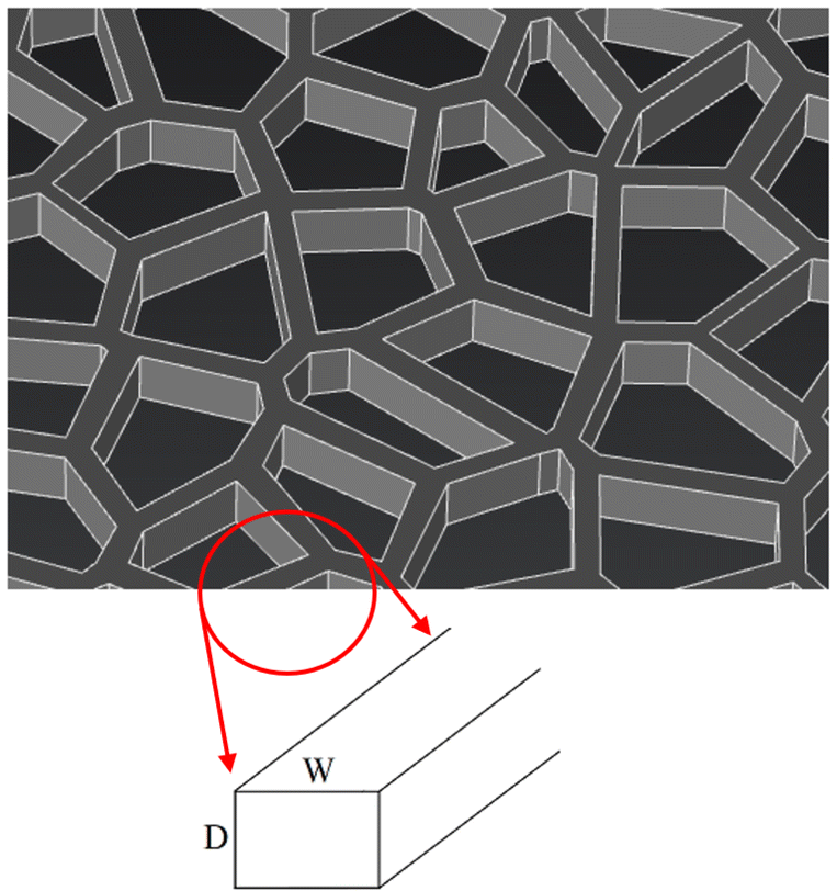 | ||
| Fig. 1 Computer-generated seamless NWN structure used in the COMSOL Multiphysics simulations for this study. The seamless nanowire segment exhibits a rectangular-shaped channel with its cross-sectional geometry characterized by the dimensions D and W representing depth and width (see inset), respectively. | ||
These seamless features tend to enrich the active percolative path fraction of the network helping to reduce the sheet resistance and increasing the light transmittance by finding its way in within void areas between the formed crack networks. Literature suggests that the best TCE-based configurations have exhibited sheet resistances of Rs ∼ 10 Ω/□ (units of Ohms per square) and optical transmittances of Top ∼ 90% in the visible wavelength range,58 however, the determined range of sheet resistance values are restricted to the particular application that the device will serve.59,60 Thermo-electro-optical performance of cracked seamless NWNs relies on various controlling parameters including the geometry of the network material such as the length of the nanowires (L), the aspect ratio (AR) defined as the width (W) divided by the depth (D) of the channel cross-sectional structure, the network area fraction (AF), and the network density (n) defined as the number of nanowires per unit of area.39,57,59,61–63 On the other hand, the thermal transport through the network depends on the thermal conductivity (kcond), the heat transfer (hconv), and the thermal emissivity (εradi) coefficients.64–66 The sheet resistance depends on the contact resistance between the network material and the device terminals and the inner nanowire resistances given by Rin = ρL/A in which A is the channel cross-sectional area, L is the length segment of the channel, and ρ is the material resistivity.59,63,67 The optical transmittance depends on the network area fraction and the associated extinction coefficient Qext as we shall detail in the Methodology section. Verifying the combined impact of such high-dimensional variable phase space on the thermo-electro-optical properties of highly disordered materials is a difficult task as one cannot rely on direct symmetry rules and nonlinear effects often do play a role. For instance, it is well understood that the AF operates as a geometrical correlation parameter between the electrical resistance and the optical transmission of the material, causing a trade-off nonlinear relationship.63,67 For this purpose, to characterize the influence of geometric aspects and intrinsic raw materials properties for quantifying the electro-optical efficiency of NWNs, a figure of merit (FOM) evaluation, commonly graphed as the optical transmittance (Top) versus the sheet resistance (Rs), is required. Investigations of the FOM of standard random NWNs made of four material compositions – silver (Ag), gold (Au), copper (Cu), and aluminium (Al) – have demonstrated that Ag displays outstanding performance compared to other alternative materials at given densities (n) and area fraction values (AF).22,33,34,59 In addition to the electro-optical response, metallic NWNs are employed for widespread applications such as displays and smart windows as transparent heaters where defogging or temperature regulation is essential.68 Hence, the thermal stability of metallic NWNs at high voltage and high-temperature conditions needs to be taken into consideration.69 Note that due to the vast number of tunable parameters considered in this work, we catalogued their names and symbols in Appendix A.
A NWN displays a heterogeneous temperature profile distribution across the network frame and rapid heating rates that lead the system to thermal equilibrium.68,70 The non-uniform temperature distribution can result in the network breakdown due to excessive temperatures concentrated at certain locations within the wire segments. Thus, estimating the local current density and thermal paths by computing the spatial electrical and thermal phenomena throughout the network is paramount for predicting device performance. Although a variety of existing high-resolution imaging techniques such as thermoreflectance70,71 and electrical mapping72 are primarily employed to capture the spatial pattern of self-heating and hotspot clustering in complex materials, such measurements are limited to evaluating local average temperatures of the networks. For this reason, accurately accessing the localized temperature distribution of individual nanowire channels experimentally can be extremely difficult at nanometer resolution.64,70,71,73,74 Zeng et al.64 have studied the electrothermal properties of nanoscale systems by simulating the local current density and temperature distributions in Ag continuous nano-crack networks. They observed significant internal temperature differences throughout the material template that can lead to junction breakdown due to thermal-assisted electronic migration mechanisms occurring in the network. Seamless networks of nano-cracks have been extensively studied experimentally.64,70,73–79 However, theoretical and computational advancements in this field are limited due to various computational challenges such as exploring a vast parameter phase space, designing and integrating the device with other circuit components, customizing raw materials for specific target applications, and modelling the coupling of distinct physical responses.64,80,81
In this manuscript, we report an in-depth computational analysis of the thermo-electro-optical properties of template-based metallic networks with seamless junctions made of different materials including Ag, Au, Al, and Cu. We determined the electro-optical properties of such networks by developing a FOM analysis with the tunning of a broad range of parameters related to the geometrical aspects of the systems which include the width (W), depth (D) and length (L) of the nanochannels as well as the network density (n), the nanochannel aspect ratio (AR = W/D), and the coverage area fraction (AF). In a seamless NWN, we define a nanochannel as a nanowire segment whose ends are randomly joined to establish a percolative complex network. The optical extinction information is calculated using finite element method (FEM) embedded in COMSOL® Multiphysics software,82 and the sheet resistance (Rs) is obtained using modified nodal analysis (MNA) for a resistive circuit network.59,83–85 Our computational framework demonstrates that template-based metallic nanowire networks have superior electro-optical performance over standard random NWNs due to their seamless nature. The electrothermal simulations were obtained using COMSOL82 to investigate the current density and temperature profile distributions with nanoscale resolution and operating at different voltage values. We have identified current density hotspots in certain regions of the network, mainly at sufficiently acute/thin nanowire intersections, caused by itinerant electrons dissipating energy at these critical locations. Our thermoelectric model shows that the spatial temperature distribution found in these networks is Weibull-governed, indicating broad electrical participation of all segment channels during the application of bias voltage. We have estimated maximum temperature values for various seamless network cases composed of target metallic materials (Ag, Au, Al, Cu) which is crucial for understanding and predicting their potential for melting/failure during an electrical operation.
This work brings a number of novelties for the community interested in NWN-based transparent conductors which include addressing seamless NWNs at the microscale dimensions and providing a systematic study of the geometrical impact in seamless NWNs over a wide range of area fraction, aspect ratio as well as network density, and performed such investigation combining three physical responses: electrical, optical, and thermal. The latter was uniquely analyzed in the form of seamless NWN temperature distributions – following Weibull probability density function – and was unified with the standard junction-based NWNs. The present study will add up to the understanding of the electro-thermal conduction transport at diffusive regimes under external stimuli or distinct operational conditions. This is particularly relevant due to the frequent occurrence of current density aggregation at specific locations in the network material, resulting in the formation of localized hotspots with elevated temperatures that may damage individual nanowires locally. This phenomenon can cause breakdowns in the network and lead to excessive average temperatures and sufficiently high sheet resistance. Moreover, this work and its extensive computational framework aim to encourage experimental fabrication at microscale sizes of seamless NWNs, which has the potential to facilitate the development of novel micro-instrumentation with improved miniaturization, thereby paving the way for advancements in the field of nanotechnology and microelectronics.
2 Methodology
To simulate the thermo-electro-optical properties of metallic seamless NWNs, we performed a two-stage approach. First, we analyzed the electro-optical performance of the network by developing a computational toolkit that derives the electrical sheet resistance and optical transmission results simultaneously. In this stage, to characterize the spatial structure of the disordered seamless NWNs, we wrote in-house codes in Python language,86 assisted by valuable network-based packages and libraries such as Shapley,87 Networkx,88 and Scipy.89 This work is primarily computational, but the design of the studied seamless NWNs is inspired by the experimental work of Sheerin et al.50,90 and many other experimental developments targeting seamless or patterned network materials.70,76,91–93 As seen in previous works,84 to generate a virtual version of a NWN in which we can perform computations, image processing methods can be applied to micrograph images of these systems from which a mapping of all their nodal, connectivity, and segment information are cast into a mathematical graph. In examining certain experimental images of seamless NWNs as studied by Sheerin et al. and other research groups,64,90,94 it was noted that a tile pattern similar to Voronoi diagrams can be utilised to replicate the structure of an experimental seamless NWN. Image processing methods are valuable tools to generate accurate geometries of NWN-based systems, but they are restricted to a limited sample size, hindering then investigations based on ensemble analysis and computation of average quantities. To obtain physical averages with statistical significance, we optimized the seamless NWN generation by considering that their network structure follows a Voronoi tessellation built upon a random distribution of centre points as shown in Fig. 2. Voronoi diagrams are used to simulate the properties of various complex systems, such as biological cells95 and cracked soils96 whose structure complexity can be captured by geometric arrangements of the so-called Voronoi cells. Thus, Voronoi cells can be considered as plane-partition polygon objects whose sides exhibit channel-like line segments randomly distributed within a squared device area of dimensions X × Y (see Fig. 2).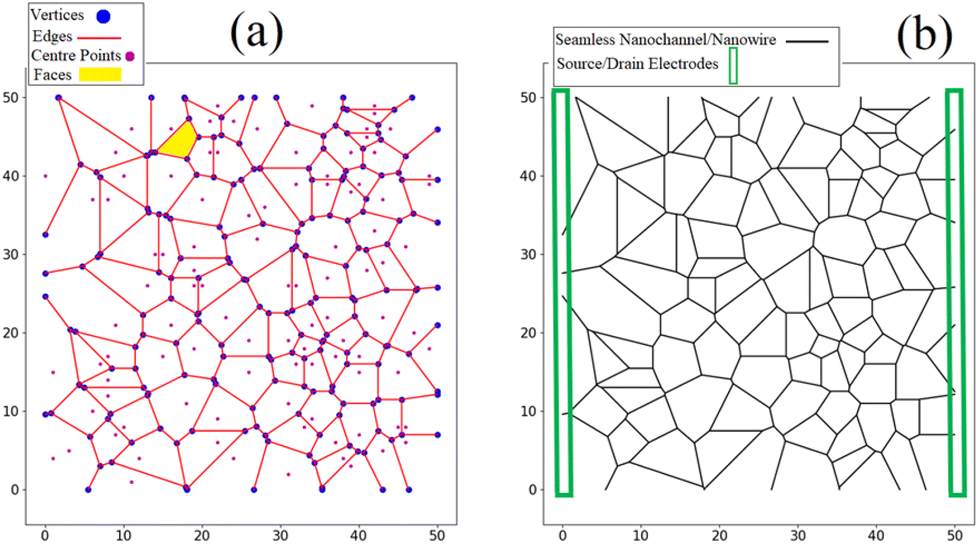 | ||
| Fig. 2 (a) A computer-generated planar Voronoi diagram. The purple dots are randomly distributed Voronoi centre points; the blue dots are the vertices that join individual line segments drawn as red lines and can also be called edges or ridges. A ridge is also referred to as a conducting nanochannel in the main text. A closed polygon or cell in the Voronoi diagram is known as a region or face and is illustrated in yellow. (b) The same Voronoi diagram in (a) is converted into a seamless NWN device in which the internal Voronoi pattern is connected to source/drain electrodes (vertical green rectangles). A percolative and transparent network is formed by a Voronoi diagram. The black line segments are the interconnected seamless nanowires. The device size is 50 × 50 μm, the density of the network is set to n = 0.05 nanowire segments per μm2, and the nanowire segments have an average length of 〈L〉 = 7 μm. | ||
Seamless NWNs are junction-free, therefore, the only entities that contribute to the overall sheet resistance of the device are the inner nanochannels resistances (Rin) along with the resistance contact points between the nanochannels and the two-terminal source/drain electrodes (Rc). As previously stated, the inner nanochannel resistances are given by Rin = ρL/A and the contact resistances Rc can be estimated based on the average of 〈Rin〉 and the electrode material. Since we prioritize the use of metallic materials, one can expect that Rc ∼ 〈Rin〉 although contact resistances between the seamless NWN and the electrodes are subject to fluctuations due to various factors, such as the electrode material, the presence of interface defects, and the specifics of the device synthesis.38 The assigned resistivity parameters used to model the metallic features of the seamless networks are ρAg = 19.23 nΩm,65ρAu = 25 nΩm,97ρAl = 62.5 nΩm,98 and ρCu = 25.51 nΩm.99 The whole network system is hence transformed into a resistive circuit network containing inner/contact resistances that connect an intricate collection of voltage nodal points that pattern a Voronoi diagram. This circuit information follows Ohm's and Kirchhoff's circuit laws that can be numerically solved for each voltage node, and ultimately calculate the overall sheet resistance Rs of the NWN. The relevant details along with the mathematical descriptions regarding our procedure used in this paper are demonstrated in our previous works.61,62,83,84,100
The optical response properties are obtained by applying FEM approach utilizing COMSOL Multiphysics package82 in which we have modelled the scattered electric field off a nanoscale object by solving Maxwell's differential equations in two-dimensional (2D) space domain. The main output of our COMSOL model is the determination of the optical efficiency coefficients defined as Qext = Qabs + Qsca in which Qext, Qabs, and Qsca stand for extinction, absorption, and scattering coefficients, respectively. The optical COMSOL analysis accomplished in this study is verified by our previous work59 in which we calculated the optical spectra of a cylinder cross-section of a nanowire exposed to direct light incidence and compared these findings with those obtained from Mie light scattering theory101,102 for an infinite cylinder. An excellent agreement was found between our optical COMSOL simulation and the Mie light scattering theory. Due to the architecture of the seamless NWNs examined in this study, whereby they are constructed with a channel-like cross-section, akin to a rectangular cross-section, rather than a circular cross-section for a cylinder. Therefore, we have exploited the overall effective optical spectra of this targeted study which is an object having a rectangular surface area in a channel-like geometry using the same technique.59 Detailed information regarding the COMSOL modelling configurations such as background electromagnetic wave, perfect electric conductors (PECs), scattering boundary conditions, object discretization into meshing, and relevant Maxwell's electromagnetic wave equations required to be solved can be found in our previous work.59 Other relevant parameters used here in our optical modelling are the wavelength-dependent refractive index information for our materials, including Ag, Au, Al, and Cu taken from Johnson and Christy103 located in COMSOL's material database. A linearly polarized plane wave perpendicularly illuminates the surface of a nanochannel situated inside a perfectly matched layer (PML) surrounded by the embedding medium, which is air in our case. The 2D electromagnetic responses were obtained using the “radio frequency” (RF) module of COMSOL Multiphysics assuming that the incident light is a plane wave and propagates in space with two orthogonal electromagnetic wave polarizations. It is worth mentioning that a difference between the standard random NWNs in our past studies and the seamless NWNs in this study is that the nanochannel segments of the seamless networks are square-shaped (not cylindrical). Nanochannel segments are viewed as cuboids deposited over a surface. The full-wave electromagnetic solutions were carried out over the wavelength range from 150 to 1200 nm for nanochannels shaped with a square cross-sectional area of sides D = 30 nm and D = 50 nm. The optical extinction coefficient (Qext) is inserted into the following equation to calculate the optical transmission (Top) of a seamless NWN:
| Top = exp{−AF×Qext} | (1) |
In the second stage of our simulations, we investigated an extended three-dimensional (3D) model of heat dissipation in a seamless NWN made of four different materials, Ag, Au, Al, and Cu. One of the purposes of this study is to understand the process of local heat transfer through the network due to heterogeneous current density profiles. The thermo-electrical properties of the complex networks are obtained utilizing COMSOL Multiphysics package82 by coupling its “electric current” (EC) and “heat transfer in solid” (HT) modules. To construct the 3D random metallic seamless films, we have generated a 2D Voronoi diagram using a DXF Voronoi pattern generator software,104 and transferred all its points and dimensions into SOLIDWORKS 2020 CAD design software105 for further manipulation. The result is a 3D Voronoi network as in Fig. 1 with a pre-defined aspect ratio (AR = W/D) described as the width-to-depth ratio of a nanochannel segment. This 3D seamless NWN structure is then imported into COMSOL Multiphysics in which we build an electrothermal model with proper meshing boundary conditions and physics laws enabled by the software. An additional figure (see Fig. S1†) detailing the meshing scheme generated in COMSOL can be found in Section 1 in the ESI.† In addition, we idealized a 3D substrate made with PET (polyethylene terephthalate) to assemble our seamless network over it, so the network is not suspended. A two-terminal set-up with electrodes made with the same metallic material as the seamless NWN structure is incorporated into the model in which a DC bias voltage can be induced to interrogate the network electrically. By increasing the applied bias voltage, we expect to yield current-induced Joule heating within the seamless NWN structure. Heat transfer equations are then solved taking into account the main intrinsic parameters that rule heat transfer mechanisms in solids as being the thermal conductivity (kcond), the convection (hconv), and the emissivity (εradi) coefficients of all objects involved in the model as well as the contact thermal conductance established between the seamless NWN and the substrate. The heat transfer equations account for three mechanisms as highlighted by previous authors:64,70 (i) thermal conduction between the seamless film and the substrate, (ii) thermal convection between the seamless film and the surrounding medium, which is air at room temperature, and (iii) thermal radiation emitted from the seamless film to the surroundings. Hence, one can write the power balance relationship for a solid object as:64,68,70,106
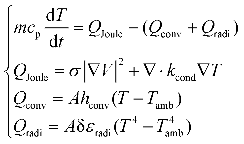 | (2) |
The precise thermal characteristics of metallic nanostructures rely on a variety of factors, including environmental and intrinsic material/geometrical features, heat transfer convection between the NWN and the environment was selected as the benchmark value for free convection of air,107hconv-air = 10 W m−2 K−1,108 and the contact thermal resistance (inverse of contact thermal conductance) between the NWN and the substrate was set to be 10−8 W m−2 K−1.109 To take into account the temperature effect on the thermal conductivity as well as the electrical resistivity during the different applied voltage, we adopted the Wiedemann–Franz law110 relationship in our modelling. Wiedemann–Franz's law proposes that the ratio of electronic thermal conductivity to electrical conductivity in metals is proportional to the temperature and will be discussed further in the next sections. More details on our considerations regarding the Wiedemann–Franz law and thermal analysis can be found in Section 2 of the ESI together with Fig. S2† which depicts the Wiedemann–Franz relationship plot of how the electrical conductivity of Ag, Au, Al, and Cu materials changes with temperature for a given thermal conductivity fixed as in Table 1 and Fig. S3† that shows how the average maximum temperature of metallic seamless NWNs increases with the bias voltage, another evidence of the electro-thermal coupling we wish to investigate in this work.
It is important to stress that in this work we consider a semi-classical (phenomenological) approach to describe the electro-optical–thermal properties of the Voronoi-based NWNs which are assumed to be at temperatures of the order of the room temperature and, despite the fact that these materials are made of numerous nanowires, we analyze their collective responses which overall compose of networks at microscale sizes (50 × 50 μm) made of multiple wire segments forming intricated pathways for the transport of the charge carriers. Moreover, the fabrication process of such networks usually does not rely on high-precision instrumentation methods to achieve pristine nanoscale architectures. As a result, their structure may also contain numerous imperfections and defects impacting the charge carriers’ trajectories. Under these conditions, we can assume that the elastic mean free path is smaller than the characteristic dimensions of the network device in which many elastic scattering events can occur while the electrons propagate through its structure. This is the case in which the charge carriers travel diffusively through the network and at elevated temperatures in which the phase coherence length is sufficiently small typically. However, the semi-classical aspect of our methodology comes from the fact that we do not use conductivity values estimated by the classical Drude model, in fact, we take these values from measurements done in nanowires whose values deviate from the classical Drude model, giving a semi-classical (and phenomenological) aspect to our description. This is how we included, in an effective way, effects associated with the characteristic nanoscale dimensions of the individual nanowires. Yet, the systems of study are in fact complex systems in the microscales as all nanowires integrate to form complex interconnects that propagate currents in their intricated network frame.
Our computational framework follows a modular structure that can navigate through four sub-modules addressing distinct responses and characterization schemes of disordered NWNs as shown in Fig. 3. The sub-modules can conduct statistical ensemble analysis of numerous NWN samples as well as customized analysis of an individual NWN structure built with very specific settings. Before going into the physical responses (electrical, optical, and thermal), an in-depth spatial characterization of the NWN structure (or an ensemble of them) is conducted using in-house scripts which give information on the network connectivity, density, junction or intersection mappings, and nanowire characteristic length distributions if applicable. This stage is required so we can establish a relationship between the structural features of the NWNs with their physical responses. This structural mapping is hence fed into the “electrical”, “optical”, and “thermal” sub-modules equipped with distinct software to extract prominent physical responses from the NWNs including sheet resistance, optical transmission, current-flow and temperature distribution profiles. To also enable the coupling of these sub-modules and their respective outcomes, we used in-house scripts written in Python programming language, SOLIDWORKS 3D CAD to design 3D NWN structures, and COMSOL Multiphysics. This schematic summarizes the computational framework followed throughout this work.
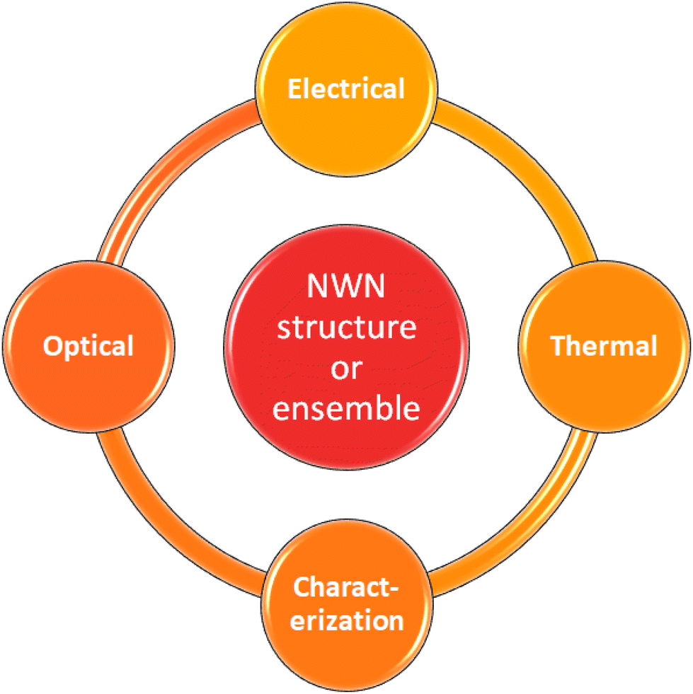 | ||
| Fig. 3 Schematic of the computational framework developed to study the thermo-electro-optical properties of disordered metallic seamless NWNs. To conduct a comprehensive analysis of the systems, it is necessary to define several key parameters related to their structural design, such as aspect ratio, area fraction, nanowire density, angular orientation, curvature, device layout, and intrinsic material properties. This is included in the spatial “characterization” module. Once these parameters are established, the next steps involve the development of computational modules for electrical, optical, and thermal simulations, employing COMSOL Multiphysics® software82 as well as in-house computational implementations to provide a thorough understanding of the behaviour of NWNs under various conditions. This whole framework is equipped to perform statistical studies in ensembles of NWNs or customized studies of individual NWN structures. | ||
3 Results and discussion
3.1 Spatial, electrical, and optical characterization
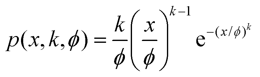
In this work, the spatial structure of seamless NWNs is based on Voronoi diagrams as illustrated in Fig. 2. Fig. 2(a) depicts the Voronoi pattern generated by a random distribution of centres (purple circles) which are encapsulated by polygons generated in accordance with the Voronoi pattern criterion. The ridges of the polygons are then viewed as nanowire segments that form a random seamless NWN structure as shown in Fig. 2(b). The NWN devices investigated here have dimensions of 50 × 50 μm and, to interrogate the network electrically, source and drain electrodes, represented by green rectangles in Fig. 2(b), are placed 50 μm apart. The aspect ratio parameter characterizing a seamless NWN, AR = W/D, is quantified from the nanowire cross-sectional area of rectangular or squared shape. Note that our seamless NWNs are generated within a fixed device area, e.g., 50 × 50 μm which characterizes typical sizes for such devices. This means that increasing the number of polygon centres results in a reduction of the average ridge length of the network. Detailed spatial characterization and statistical analysis performed in an ensemble of computer-generated seamless Voronoi NWNs are presented in Fig. 4. Histograms of perimeter and ridge lengths plus polygon area were obtained for an ensemble of 1000 Voronoi NWN samples generated with 500 centres. All Voronoi samples were confined within an area of 50 × 50 μm. These histograms enable us to determine typical length and area scales of the finite-size Voronoi networks we wish to characterize electrically later. This result intends to provide an understanding of the main spatial features of the disordered Voronoi NWNs targeted in this study for subsequent analysis of their electro-optical–thermal properties. The distributions plotted in histogram form give information about the collective spatial characteristics of a large ensemble of Voronoi NWNs so we can have a picture of their main spatial features and typical length scales. Note that the Y-axes of the histograms are labelled as ‘density’ meaning that the integration over the probability density function at the bin is normalized to one. We verified, as in previous works, that the polygon area distribution fits well with a two-parameter Gamma distribution111,112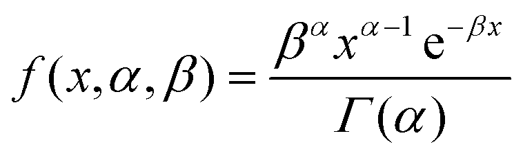 | (3) |
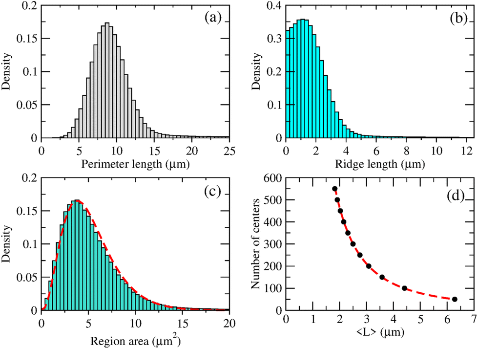 | ||
| Fig. 4 Spatial characterization conducted on an ensemble of 1000 Voronoi NWNs built with randomly generated centre points from which the ridges/polygons are drawn. Panels (a–c) are histograms of perimeter length, ridge length, and region area, respectively, obtained for 1000 Voronoi NWNs generated with 500 randomly distributed centre points. All Voronoi samples were confined within an area of 50 × 50 μm. The Y-axes of the histograms are communicated in terms of ‘density’ meaning that the integration over the probability density function at the bin is normalized to one. Panel (d) depicts how the number of Voronoi center points (Nc) varies with the average ridge length, 〈L〉. Dashed lines on panels (c and d) correspond to fittings of: (c) Gamma distribution as given in eqn (3) in the main text and (d) a power law given by Nc = C〈L〉γ. The fitting parameters are α = 3.66 (Gamma distribution shape parameter), β = 0.7 (Gamma distribution inverse of scale parameter), and the power law parameters, C = 1800 and γ = −1.95. | ||
Before presenting the complete FOM trade-offs in seamless NWNs, we need to calculate the optical extinction coefficient, Qext, that characterizes the intrinsic optical properties of the nanowires composing the networks. It is also worth mentioning that we attempted to perform a direct comparison of our quantitative results that will be presented later on with other works in the literature. This is to make sure that our computational framework is tuned with past predictions conducted theoretically/computationally and experimentally. This comparison can be found in Section 4 of the ESI with the supporting Table S1.†Fig. 5 shows the spectral extinction results obtained using COMSOL for incident wavelengths ranging from 200 nm to 1250 nm for Ag, Au, Al, and Cu nanowire materials. The target orientation was adjusted such that the primary axis of the square-shaped nanowire is perpendicular to the propagation of the incident wave. We have computed and averaged both orthogonal polarizations of the incident beam, one with an electric field normal to the square-shaped nanowire axis and the other with an electric field parallel to it. We also contrasted optical extinction effects for nanowires of distinct cross-sectional shapes: squared and circular (see also Fig. S4 and S5 in Section 3 of the ESI†). These two shapes are characterized by distinct length scales and cross-sectional areas: square-shaped nanowires have cross-sectional area given by A■ = W2 = D2 whereas circular-shaped (cylindrical) nanowires have cross-sectional area given by A○ = π(d/2)2 with d being the diameter of the circle. Optical extinction spectra were obtained by fixing these two relevant length scales (D = W and d) to 30 nm and 50 nm to visualize the light scattering effects caused by widening the nanowire thickness. As can be observed, the optical extinction spectra throughout the specified wavelength range not only behaves distinctly primarily due to the alteration of raw materials but also change with respect to the length scales and nanowire shape. Overall, square-shaped nanowires impart more extinction than cylindrical ones which will play an important role in the computation of the optical transmission of seamless NWNs. In general, the relative electric field intensities at a square cross-section (assigned to a square nanochannel) and a circular cross-section (assigned to a cylinder nanowire) have risen for nanomaterial structures made of Ag, Au, Al, and Cu (see Section 3 in the ESI†).
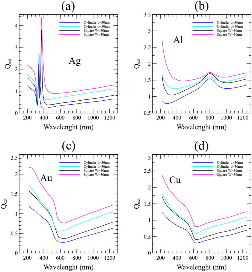 | ||
| Fig. 5 Wavelength-dependent optical extinction coefficients (Qext) over the range of 200 nm to 1250 nm obtained for distinct metallic materials: (a) Ag, (b) Al, (c) Au, and (d) Cu. These results were computed via COMSOL model with the electromagnetic wave's propagation along the Y-axis, and its polarizations along the X- and Z-axes. Nanowires of different cross-sectional shapes were modelled: a square-shaped nanowire of width W = D = 30 nm and 50 nm, and a cylindrical nanowire of diameter d = 30 nm and 50 nm. | ||
The electric field scattering planar profiles are calculated using COMSOL and displayed in Fig. 6 for a square-shaped nanowire made of distinct metals exposed to a light wave of λ = 550 nm propagating along Y-axis with two normal polarizations along X- and Z-axis. The square in the center of the panels is the cross-section of the nanowire. A direct comparison with the electric field scattering obtained for cylindrical nanowires is presented in the ESI, Fig. S4 and S5.† The squared edges certainly play a role in the electric field attenuation caused by the nanowire. Since the electric field is proportional to the charge density, nanochannels with sharp vertices depict intense electric fields at the tips (“tip effect”), which indicates high charge densities. We detect an increase in optical attenuation and a larger scattering electric field as a consequence of the inhomogeneous distribution of the local electric field around the nanowire square cross-section, except for Al,113 which is generated by induced electric dipole resonance. The electric field inside the Al nanowire is nearly zero, indicating that the distribution of electrons subjected to an external electric field results in the polarisation of negative and positive charges on opposite edges of the nanochannel; the field produced by these partitioned charges cancels out the external field inside the conductor. This dipole moment generation and dipole strength are determined by the polarizability of the material as well as heavily reliant on the shape, size, and dielectric environment of the nanowire.114 In addition, the surrounding relative electric field strengths between the square cross-section (belonging to a squared nanowire) and the circular cross-section (belonging to a cylinder nanowire) convey a field enhancement of approximately 1.2, which clarifies why the computed extinction coefficients are sufficiently larger for the squared-shape nanowires115 as depicted in Fig. 5.
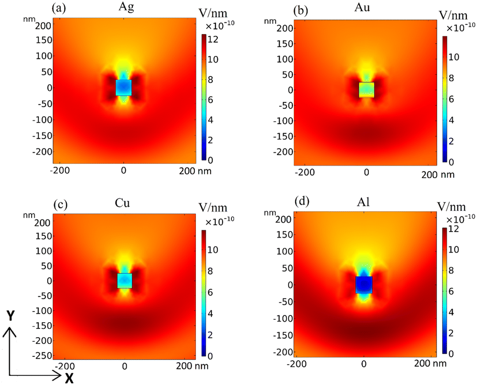 | ||
| Fig. 6 The electric field distribution around the square cross-section in the X–Y plane of a nanowire. The nanowires are composed of (a) Ag, (b) Au, (c) Cu, and (d) Al with D = 50 nm. The square geometry is illuminated by a plane wave of λ = 550 nm whose direction of propagation is along the Y-axis with two normal polarizations along X- and Z-axis. The colour bar displays the electric field intensity (V nm−1) simulated according to the mean of two perpendicular electric field polarization. | ||
The trade-off between optical transmission and sheet resistance for seamless NWNs generated as Voronoi diagrams is presented in Fig. 7. This result was obtained for an ensemble of seamless NWNs containing 50 samples and each point on the panel was calculated for a fixed number of centre points randomly distributed over a 50 × 50 μm surface area. In descending order of resistance values, Nc was varied from 25 to 300 in steps of 25. We considered two types of materials to contrast their FOM, Ag and Al. The Voronoi networks were converted into a weighted mathematical graph made of voltage nodes and edges in which the weights are the inner wire resistances; to eliminate the dependency on the contact resistances, the extended electrodes in Fig. 2(b) were assigned to the furthest left node (source) and the furthest right node (drain) in the Voronoi structure. The overall sheet resistance of the network is obtained by computing the ‘resistance distance’ associated with the graph. The optical transmittance is calculated using eqn (1) with Qext taken from Fig. 5, tuned to the visible wavelength of 550 nm, and the area fraction obtained from the top-view computer-generated Voronoi images. Our model predicts the expected trends in terms of control parameters; seamless networks made of less resistive materials and larger cross-sectional areas are promising electrical conductors, with square-shaped Ag NWNs of W = 50 nm exhibiting 〈Rs〉 < 200 Ω. This gain in electrical conductance in comparison with the W = 30 nm case shows a reduction in optical transmission, with smallest computed transmittance values ≈97%. The high resistivity of Al combined with its large extinction properties make Al seamless NWNs branch at larger resistance ranges and lower optical transmission values than the Ag seamless NWNs. Yet, our model predicts optical transmissions above 90% for all studied parameters, confirming in quantitative terms that seamless NWNs are promising candidates for transparent conductor applications.
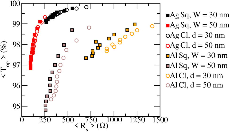 | ||
| Fig. 7 Figures of merit relating the average optical transmission with the average sheet resistance obtained for ensembles of Voronoi seamless NWNs of distinct shapes and materials. The averages were taken over an ensemble of 50 Voronoi NWN samples. Two material types were tested: Ag and Al. The cross-section of the Voronoi ridges can be square- (Sq, filled square symbols) or circular-shaped (Cl, hollow circular symbols). Two characteristic ridge dimensions were investigated, 30 and 50 nm, as displayed in the legend. In the case of squared ridges, the dimension refers to their depth = width denoted by D = W, whereas for cylindrical ridges with circular cross-sectional areas, the dimension refers to their diameter denoted by d. | ||
However, one can wonder: how does the overall performance of seamless NWNs compare with junction-based random NWNs? The latter is characterized by a connectivity profile of interwire junctions which yield an extra resistance contribution on top of the wires’ inner resistances. Additionally, junction-based NWNs have wire segments that are essentially ‘dead ends’ which do not contribute to the conduction process but do contribute to the area fraction. Seamless and junction-based NWNs cannot be compared directly since their connectivity and nodal configuration differ considerably due to their built-in designs. Junction-based NWNs carry a 3D element to their connectivity profile due to their transversal interwire junctions. Yet, it is possible to make a qualitative comparison on the typical orders of magnitude their sheet resistances and optical transmission can reach. The electro-optical performance of two different NWNs, namely seamless and standard (junction-based), is compared in Fig. 8. This figure presents the results for optical transmittance versus Rs with a device dimension of 20 × 20 μm with nanowires made of Ag. The NWN insets correspond to snapshots of two comparable NWNs (junction-based in green and seamless in red) in terms of area fraction with nanowire's average length 〈L〉 = 4.6 μm. The standard NWNs are composed of cylindrical nanowires with a fixed diameter of d = 50 nm whereas the seamless NWNs consist of Voronoi templates with ridges of square shape of fixed depth D = 50 nm. In addition, even though the computed Qext for seamless square-shaped nanowires tends to be greater than those with circular cross-sections (see Fig. 5), the projected transmittance indicated in Fig. 8 is greater for seamless NWNs owing to their sufficiently low area fraction. In a standard NWN, the prerequisites for a connection between two sticks are that their centres be within L of one another, where L is the length of the sticks, and their relative direction is such that they intersect. According to Pike and Seager,116 the critical density of randomly oriented 2D sticks can be determined by (nw)cL2 = B where (nw)c is the network's nanowire critical density to percolate spatially and B ≈ 5.7. Consequently, for a complex system to effectively percolate, a standard NWN must fulfil this criterion but, in a seamless NWN, no such conditions exist because the system template is already structured to percolate the electrodes. This comes as an extra advantage linked to the seamless NWNs over the standard random NWNs. The agreement between our simulated results and the observations made by Kumar et al.57 for comparison between seamless and standard NWN indicates that the simulation methodology employed in this research is able to capture the key aspects of the system responses.
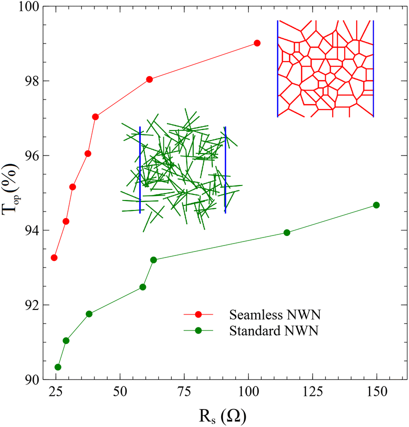 | ||
| Fig. 8 Optical transmittance (Top (%)) versus sheet resistance (Rs) of seamless and standard (junction-based) NWNs made of Ag. The diameter of cylindrical nanowires for the standard NWNs is d = 50 nm and the depth of the nanochannel for seamless NWNs is D = 50 nm. The widths of the seamless NWNs are varied from W = 50 nm to W = 350 nm to match the AF of the standard NWNs and to obtain the selection of points shown on the plot. All systems are 20 × 20 μm in size. Each data point represents the mean of 10 ensembles of random spatial configurations. The junction resistance between two nanowires in standard NWNs and the contact resistance with the source/drain electrodes are all set to Rc = Rjxn = 10 Ω.38 The NWN insets correspond to snapshots of two comparable NWNs (junction-based in green and seamless in red) of nanowire's average length 〈L〉 = 4.6 μm. | ||
3.2 Electro-thermal characterization
In this part, we discuss the results found using the electro-thermal steady-state modelling in COMSOL Multiphysics software,82 compared with those obtained numerically using in-house scripts. Additional physical quantities can now be calculated with COMSOL such as temperature, electrostatic potential, and current density. As a result, the relation between the network geometry and electric/thermal properties can be shown. To ensure that our COMSOL seamless NWN model agrees with our in-house scripts that provide electrical properties, we calculated the sheet resistance using both computational COMSOL Multiphysics and probed the sheet resistance trend at fixed AR while varying AF, and vice versa. This comparison is presented in Fig. 9; where the agreement between the two computational techniques is clearly observed. The electrical and thermal conductivity specifications for both approaches are taken from Table 1. Note that Fig. 9(b) shows a seemingly non-intuitive behaviour of sheet resistance increasing with the nanowires’ aspect ratio. However, it is worth mentioning that generating Voronoi networks to feed the COMSOL Multiphysics has its challenges, particularly Voronoi networks of finite sizes as considered in this work. The result in Fig. 9(b) omits the fact that the density (number of ridges per unit of area) of the Voronoi networks is not constant when the system boundaries are fixed at 50 × 50 μm. The sheet resistance is increasing with AR because the generated seamless Voronoi networks also get sparser in terms of ridge number and lengths.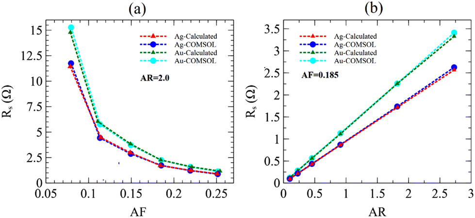 | ||
| Fig. 9 Sheet resistance (Rs) obtained systematically for seamless Voronoi NWNs by (a) varying AF and fixing AR, and (b) vice versa. Two computational methods were used to determine the quantities: COMSOL Multiphysics (circular symbols, labelled as ‘COMSOL’) and our in-house scripts based on circuit networks and Kirchhoff's circuit laws (triangular symbols, labelled as ‘calculated’). All systems are 50 × 50 μm in size and two distinct raw materials were probed, Ag and Au. The sheet resistances determined via in-house scripts are average values obtained for an ensemble containing 10 random spatial Voronoi configurations, but for the COMSOL results, each data point corresponds to a single imported CAD design. | ||
To perform the thermal characterization alongside the electrical analysis, we used the Wiedemann-law Franz's relationship110,117 (see also Section 2 in the ESI†) that relates electrical and thermal conductivity, so we can study the impact of Joule heating and, eventually, map how the local current density and temperature gradient profiles in the seamless NWNs distribute under different supplied voltages. According to the Wiedemann–Franz law, the ratio of a metal's thermal conductivity (kcond) to its electrical conductivity (σ) is proportional to its temperature (T) and can be written as 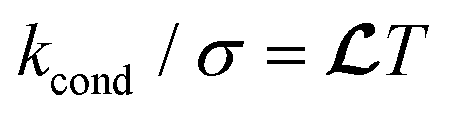 in which
![[thin space (1/6-em)]](https://www.rsc.org/images/entities/char_2009.gif) 110 is the Lorenz number given by
110 is the Lorenz number given by  . Fig. 10(a) displays the network formed by the Voronoi diagram imported in COMSOL for electrothermal modelling. The aspect ratio and area fraction of the networks can also be altered to analyze the influence of network geometry on the film characteristics as discussed in this paper. Fig. 10(b) depicts the modelled spatial electrostatic potential. The vertical lines at the extremes of the network represent electrodes with an induced voltage difference of 1.6 V. Nanoscale ridges made of Ag were distributed within a 50 × 50 μm area following a Voronoi algorithm. We observe the electrostatic potential drops approximately linearly across the device length from 0 (ground, left) to 1.6 V (right).
 | ||
| Fig. 10 (a) Schematic diagram of a seamless conductive NWN model generated with the COMSOL Multiphysics software.82 The random seamless network is represented by a Voronoi diagram built within a 50 × 50 μm area and deposited on a substrate (grey cuboid). (b) Calculated surface electrostatic potential ranging from 0 V to 1.6 V bias voltage sourced to the same seamless NWN shown in (a) and considering that its ridges are made of Ag material. The colour gradient demonstrates that the electric potential grows consistently from left (dark blue) to right (red) based on their respective nominal terminals (vertical lines at the extremes of the device), ground and source, respectively. | ||
Sheet resistance and the network average temperature were examined by varying the applied voltage from V = 0.1 V to V = 4.6 V in increments of 0.5 V. Fig. 11 top panels (a and b) depict the sheet resistance versus applied voltage for Ag and Au seamless NWNs, respectively, with fixed AR = 2.0 and variable AF = 0.08 to 0.25 while bottom panels (c and d) show the results for fixed AF = 0.185 and various AR = 0.1 to 3.0. These results were calculated using COMSOL Multiphysics. Similarly, Fig. 12 shows the simulated results of sheet resistance versus applied voltage for different AR and AF associated with other seamless network materials, Al and Cu. Comparing Fig. 11 and 12 suggests that under similar network geometry and applied voltage, the sheet resistance is both thermally and electrically material sensitive. For instance, although the electrical conductivity of Cu is set to be greater than that of Al by a factor of 2.5 (see Table 1), Al sheet resistances range in lower values (2–40 Ω) than for Cu NWNs (2–80 Ω) within the same range of applied bias voltage. This increase in sheet resistance for Cu seamless NWNs, as opposed to its higher electrical conductivity, is attributed to the fact that Al thermal conductivity is roughly 1.8 times larger than Cu, assuming the values reported in ref. 99 of kcond-Cu = 65 W m−1 K−1 and the ones reported in ref. 98 of kcond-Al = 120 W m−1 K−1. In nanostructured seamless films, in addition to the material's intrinsic characteristics such as thermal conductivity (kcond) and electrical conductivity (σ), heat transfer convection (hconv), aspect ratio, area fraction, and NWN density also serve as primary mechanisms for tailoring the sheet resistance as shown in Fig. 11 and 12. By coupling electrical with thermal properties, we can also demonstrate that the same phase space parameter can be used to tailor the average temperature of the NWNs. When a voltage is applied across a resistor, a current flows through the resistor, and energy is dissipated in the form of heat. This heat raises the temperature of the resistor; in the case of the seamless NWNs composed of multiple nanoscale resistors, we quantified the average temperature increase of the entire network as can be seen in Fig. 13. This phenomenon is known as Joule heating. As the temperature of the network increases, the electrical conductivity (σ) of the resistors decreases due to the Wiedemann–Franz law, which states that the electrical conductivity of a material is inversely proportional to its temperature when the thermal conductivity (kcond) is constant (see Section 2 in the ESI†). Therefore, as the temperature of the network increases due to Joule heating, the electrical conductivity of its resistors decreases, leading to an increase in the overall resistance of the network, and further increasing the amount of heat generated.106,110,117,118 This is the assumption we have established in our COMSOL Multiphysics modelling as the literature suggests that the fluctuation in electrical resistivity (inverse of electrical conductivity, ρ = 1/σ) is greater than the fluctuation in thermal conductivity as temperature varies (e.g., within the temperature range of 50–300 K for Ag,65kcond(300 K)/kcond(50 K) ≈ 1.6 while ρ(300 K)/ρ(50 K) ≈ 4.0).65,97–99
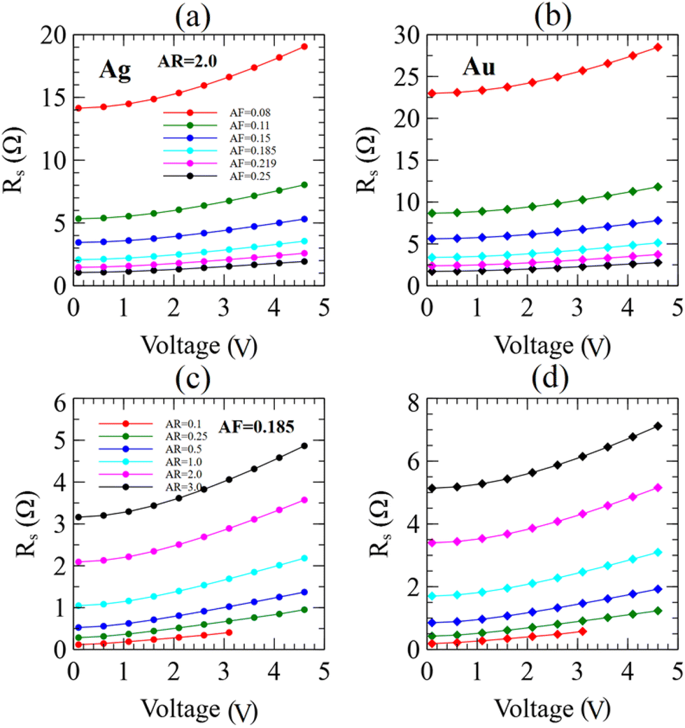 | ||
| Fig. 11 Calculated sheet resistance (Rs) versus applied voltage results obtained with COMSOL. All systems are 50 × 50 μm in size. Each data point corresponds to a single imported seamless NWN CAD design for COMSOL modelling. (Top panels) Rsversus bias voltage for seamless (a) Ag and (b) Au NWNs with fixed AR = 2.0 and various densities and AF values. (Bottom panels) Rsversus bias voltage for seamless (c) Ag and (d) Au NWNs with fixed AF = 0.185 and various densities and AR values. | ||
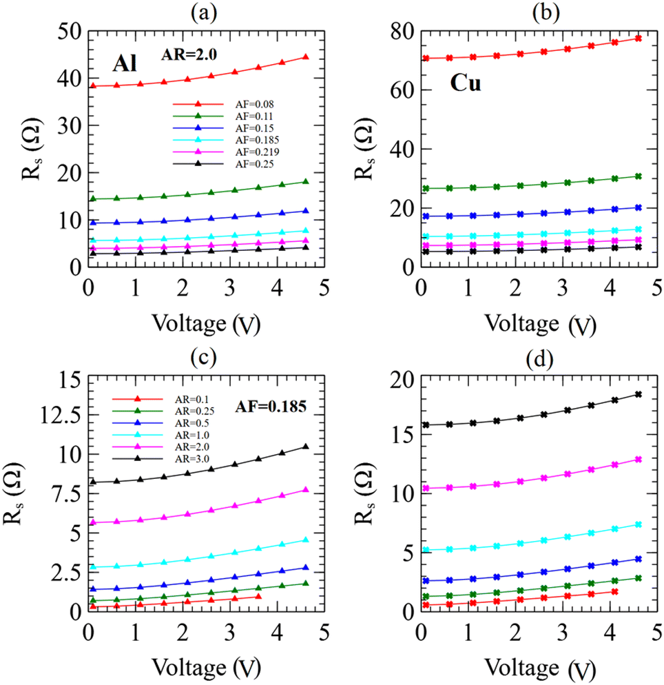 | ||
| Fig. 12 Calculated sheet resistance (Rs) versus applied voltage results obtained with COMSOL. All systems are 50 × 50 μm in size. Each data point corresponds to a single imported seamless NWN CAD design for COMSOL modelling. (Top panels) Rsversus bias voltage for seamless (a) Al and (b) Cu NWNs with fixed AR = 2.0 and various densities and AF values. (Bottom panels) Rsversus bias voltage for seamless (c) Al and (d) Cu NWNs with fixed AF = 0.185 and various densities and AR values. | ||
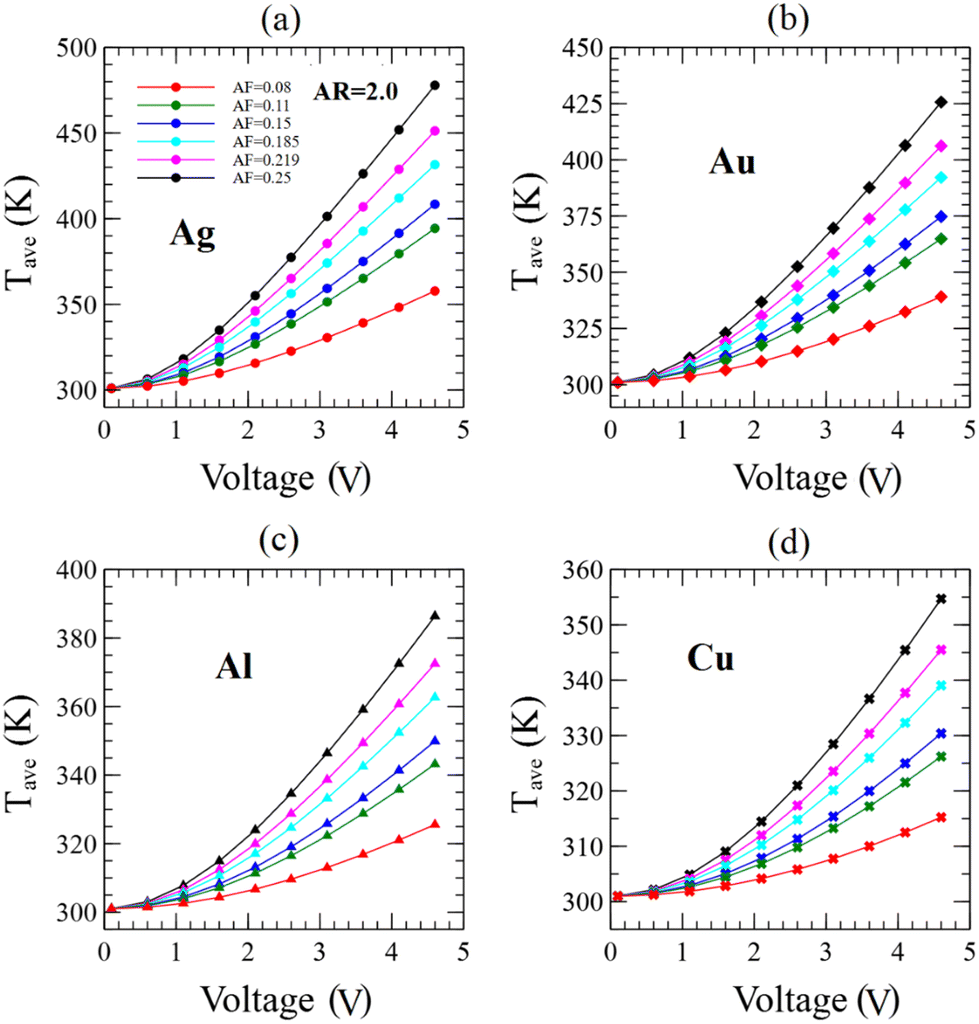 | ||
| Fig. 13 Calculated average network temperature (Tave) in Kelvin (K) versus applied voltage (V) results for seamless NWNs made of distinct metals, (a) Ag, (b) Au, (c) Al, and (d) Cu. All systems are 50 × 50 μm in size. Each data point corresponds to a single imported seamless NWN CAD design for COMSOL modelling. For all panels, the ridge aspect ratio was fixed at AR = 2.0 and distinct curves correspond to different area fraction values as specified on the legend in panel (a). | ||
Our seamless NWNs models evidence the lowest sheet resistances of Rs ≈ 1 Ω to the highest at Rs ≈ 80 Ω by modifying the metallic composition of the NWNs and their network/structural properties. It is also interesting to note the nonlinear trend of the sheet resistance as a function of bias voltage depicted in all cases in Fig. 11 and 12. Fig. 13 shows the network average temperature versus different applied bias voltages for fixed AR = 2.0 and varied area fractions from AF = 0.08 to AF = 0.25 for Ag, Au, Al, and Cu seamless NWNs. This result indicates that under similar device specs and network architecture, Ag and Au exhibit higher temperature values than Al and Cu. Overall, our predicted sheet resistances (see Fig. 11 and 12) and network average temperatures (see Fig. 13) are sensitive to material and network layout, and our numbers are within the same orders of magnitude as other reports in the literature.64,68–70,72,73,94,119–121
The contact thermal conductance between the NWN and the substrate is an additional factor addressed in this work that influences the temperature profile distribution inside the metallic seamless NWNs and, subsequently, the sheet resistance. In nanodevices, the contact/interfacial thermal resistance (inverse of contact thermal conductance) plays a major part in the transfer of thermal energy. Integration of nanoelectronics requires a comprehensive knowledge of nanoscale interfacial heat transport phenomena.109,122,123 To probe the impact of contact thermal conductance between the metallic seamless NWN and the substrate on sheet resistance and network average temperature, we varied this quantity as depicted in Fig. 14. In this particular examination, we fixed AR = 2.0 while varying the contact thermal conductance to compare the computed results for several selective case studies including AF = 0.185 and 0.25, and bias voltages of V = 1.1 V and 2.6 V for Ag and Au seamless NWN materials. The contact thermal conductance can vary considerably depending on the nanostructure and material manufacturing; consequently, we choose the most typical range described in the literature for metallic nanowires, which is from ∼107 to ∼108 W m−2 K−1.109,122 The result shown in Fig. 14(a) and (c) emphasises that the average network temperature decreases as the contact thermal conductance rises. It is known that the electrical conductivity rises with decreasing temperature as predicted by the Wiedemann–Franz relationship. Additionally, increasing the contact thermal conductance means improving the thermal coupling between the network and the substrate. As a result, the network is able to “cool down” upon such improved contact. Fig. 14(b) and (d) also show the reduction in sheet resistance that supports this explanation. Disordered nanomaterials such as seamless NWNs can exhibit significant pockets of heat which are also referred to as hotspots and will be discussed later. Hence, this finding suggests that the contact thermal conductance can be used as another tuning parameter for controlling the thermal and electrical characteristics of seamless NWNs.
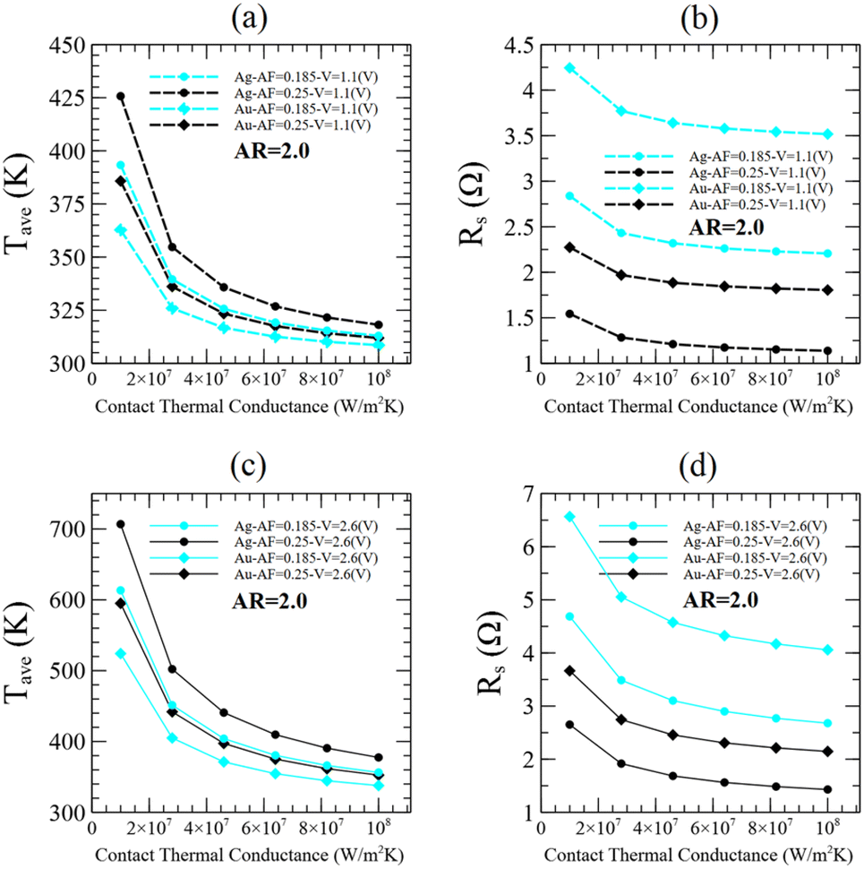 | ||
| Fig. 14 (a and b) Calculated average network temperature (Tave) and sheet resistance (Rs) versus contact thermal conductance results for V = 1.1 V, fixed AR, distinct area fraction values, and distinct metals (Ag and Au). (c and d) Calculated average network temperature (Tave) and sheet resistance (Rs) versus contact thermal conductance results for V = 2.6 V, fixed AR, distinct area fraction values, and distinct metals (Ag and Au). All systems are 50 × 50 μm in size. Each data point corresponds to a single imported seamless NWN CAD design for COMSOL modelling. The tuning parameters include the fixed AR = 2.0, AF = 0.185 and 0.25, and V = 1.1 V, displayed with dash lines, and V = 2.6 V, displayed with solid lines. The chosen materials include Ag, depicted with circle symbols, and Au, depicted with square symbols. | ||
The percolated structure and undisrupted connection layout of seamless NWNs permit a more detailed spatial analysis in terms of color maps that evidence how certain quantities distribute over their nanowire segments. Fig. 15 illustrates the distribution of local current density and temperature profile for a seamless NWN obtained via COMSOL. Electrical breakdown processes within the nanowire network can occur when any active percolative nanowire hits its critical melting temperature, disrupting current flow and resulting in an abrupt change in sheet resistance. The color code used in Fig. 15 identifies red spots as critical nanochannels or intersections that have attained high current densities or temperatures in our electrothermal COMSOL modelling. The electric current density and temperature profile distribution throughout the network depend on the applied voltage. Fig. 15(a) displays the electrostatic potential drop as expected for a heterogeneous percolated metallic network subjected to a two-terminal electrode setup. For the other quantities mapped in Fig. 15, we can see that the network sets a heterogeneous environment for current flow and temperature distribution; (conventional) current flow occurs from source (positive) to drain terminals represented by vertical lines positioned at the far left and right locations of the device. For this reason, large current densities are concentrated at ridges oriented nearly horizontally or nearly aligned with the direction of the electric field established by the voltage difference at the terminals. Such nanoscale ridges (overloaded with current) are prone to melting and failure due to Joule heating.64 Regions with high current densities (see Fig. 15(c)) tend to be ‘hotter’ as observed in Fig. 15(b) depicting the temperature distribution across the network. Running the same model for distinct seamless NWNs of different geometries, it is possible to obtain temperature distributions which could indicate the likelihood of sensitive ‘hotspots’ in the networks as also depicted on the bottom panels of Fig. 15 zooming at particular sections of the network.
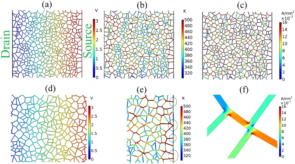 | ||
| Fig. 15 Color maps taken from the electrothermal COMSOL modelling of an Ag seamless NWN. Panel (a) depicts the electrostatic potential established between source and drain electrodes, panel (b) depicts the temperature distributed across the same network, and panel (c) depicts how the current density spreads across the same network. (d) Magnified view at the central section of the network in panel (a) depicting how the electrostatic potential is distributed. (e) Magnified view at the right electrode of the network in panel (b) depicting how temperature varies in the vicinity of the electrode. The circles highlight critical ‘hotspots’ of high temperatures colored in red. (f) Magnified view at a seamless segment from panel (c) exhibiting high current densities colored in red. The seamless NWN is 50 × 50 μm in size, AR = 1.0, AF = 0.185, and ΔV = 3.1 V. | ||
Understanding the device's conduction routes and the physical aspects that restrict performance, especially in relation to electrothermal fracture, are both aided by high-spatial-resolution measurements of variation in temperature across the network regions.71 For this reason, the temperature profiles calculated using COMSOL simulation (see Fig. 15(b)) for computer-generated seamless NWNs of fixed AF = 0.185 and AR = 3 were mapped into probability distributions that can be fitted with probability density functions (PDFs) of temperature differences (ΔT) as shown in Fig. 16. In this context, the variation in temperature, ΔT, is characterized as the result of subtracting the simulated temperature from ambient temperature, as defined in our simulations. The networks made of Ag, Al, Au, and Cu nanowire ridges were subjected to a bias voltage of 4.6 V and numerous temperature mappings were obtained using COMSOL from which the temperature difference distributions were determined. Our fitting analysis confirms that all distributions follow a two-parameter Weibull distribution defined as
 | (4) |
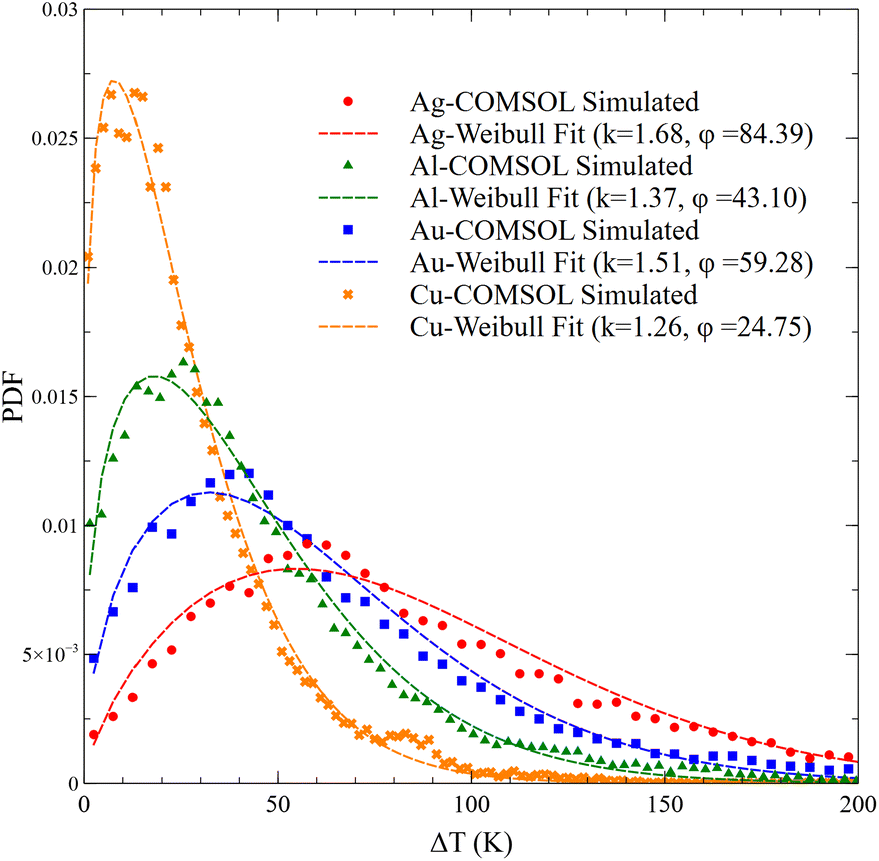 | ||
| Fig. 16 (Symbols) Temperature difference distributions obtained for seamless NWNs made of distinct metals, AF = 0.185 and AR = 3 and fixed voltage at 4.6 V. These were obtained using COMSOL Multiphysics set for electrothermal simulations. (Dashed lines) Fitting of Weibull probability density function (PDF) for each case study. The values of the fitting parameters are presented in the legend. | ||
Let's now breakdown and interpret the results presented in Fig. 16; the shapes of the PDFs are mostly right-skewed, showing that, for a given bias voltage, the temperature of the majority of the nanowires, actively participating in the propagation of current, rises with regard to the original temperature setting. In addition, this result depicts that the Weibull fitting parameters are material-dependent which can be analyzed in terms of the overall electrical current flowing through the network which will be discussed later. From the main characteristics of a Weibull PDF, we can observe interesting features from material to material; for instance, Ag seamless NWNs exhibit a wider temperature change spread with a mode at ∼55 K whereas Cu seamless NWNs exhibit less spread with a mode located at ∼7 K. Weibull PDFs normally describe random variables that are identified as “time-to-failure” and, depending on the value of the exponent k, we can obtain information about the failure rate of the system being studied. For instance, k > 1 indicates that the failure rate increases with time as a result of “aging” in which parts of the system can wear out as time goes by. In our case, the random variable is ΔT or “ΔT-to-failure” meaning that the “aging” process is temperature driven. All NWNs in Fig. 16 depict k-values indicative of failure rates that increase with temperature change. We can estimate the mean temperature-change to failure (〈ΔT〉f) through the definition of the mean of a Weibull PDF which is
 | (5) |
The mode and the mean temperature-change to failure for each seamless NWN displayed in Fig. 16 are presented in Table 2. The numbers show that the Ag NWN exhibits the highest mean of ≈84 K whereas the Cu NWN exhibits the lowest mean of ≈24 K. Our interpretation of this difference is that the Ag NWN is capable of sustaining larger temperature variances due to its effective current/temperature spreading mechanism as evidenced by its Weibull shape. That does not seem to be the case for the Cu NWN in which its self-heating mechanism and material attenuation can span lower temperature ranges, however, its spreading is not effective to sustain sufficiently larger temperature-changes, making them more prone to electrothermal failure.
| Material | Mode (K) | 〈ΔT〉f (K) |
|---|---|---|
| Ag | 55.16 | 84.39 |
| Au | 32.02 | 59.28 |
| Al | 18.12 | 43.10 |
| Cu | 7.61 | 24.75 |
Finally, a direct investigation of the Weibull parameters obtained from the fitting in Fig. 16 (at fixed 4.6 V) and from another thermal study we conducted for the same systems but fixing the voltage at 1.1 V is presented in Fig. 17. The Weibull analysis for the second case study can be found in the ESI, Fig. S6 in Section 5.† In these plots, we used the overall current flowing through each seamless NWN (of different materials) as the proxy for this analysis. Following the current in a crescent order, the symbols in the plot (for both voltage values) correspond to the distinct metals in the following order: Cu → Al → Au → Ag. The currents were obtained simply with Ohm's law Im = V/Rm in which V is the fixed voltage depicted in the legend and Rm is the electrical resistance obtained from the COMSOL model for each material (m = Cu, Al, Au, Ag). We can see that both Weibull parameters (k and ϕ) evidence clear linear trends with the current, with the scale parameter, in particular, depicting a scaling feature with the fixed voltage. The fitting on panel (a) is given by y = cx + b in which the ordinate information is ϕ/Vγ and the abscissa is the current Im. The scaling exponent γ was adjusted to visually align both linear trends as depicted on the panel and that was found at γ = 1.27. The slope and the linear shift obtained for both high (Vh = 4.6 V) and low (Vl = 1.1 V) voltage regimes are given by ch ≈ cl ≈ 14 and bh = 0.477, bl = 0.129. No voltage scaling was determined for the shape parameter k depicted on panel (b) since their slope alignment is already evident. The slope and the linear shift obtained in this case are ch ≈ cl ≈ 0.61 and bh = 1.108, bl = 1.011. In summary, the analysis in Fig. 17 generalizes the Weibull thermal response of seamless NWNs, made of distinct metals, in which their parameters can be estimated by a linear extrapolation of the models here presented. Section 5 in the ESI† also contains an additional Weibull temperature analysis conducted in seamless metallic NWNs of distinct geometrical features to also observe the effect of the thickness of the nanoridges on temperature variation distributions (see Fig. S7†). However, due to the already substantial analysis gathered in the main text, we left that result and related discussion in the ESI† of this work.
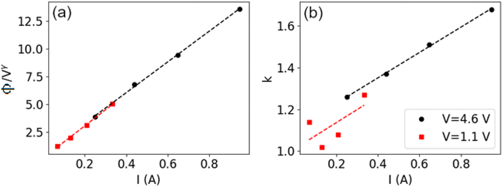 | ||
| Fig. 17 Analysis of the Weibull fitting parameters (ϕ, k) obtained in Fig. 16 in terms of voltage and materials’ differences. The current in both panels is the proxy that indicates material change; in a crescent order, the symbols in the plot (for both voltage values) correspond to the following order: Cu → Al → Au → Ag. In both panels, black circles are the data representing a high voltage regime (Vh = 4.6 V) whereas red squares are the data representing a low voltage regime (Vl = 1.1 V). The dashed lines are linear fits given by y = cx + b. The slope and the linear shift found in all linear fittings are: (a) ch ≈ cl ≈ 14 and bh = 0.477, bl = 0.129. In this analysis, the scale parameter ϕ was scaled by Vγ to visually align the trends for distinct voltage values. The scaling exponent was found γ = 1.27; (b) ch ≈ cl ≈ 0.61 and bh = 1.108, bl = 1.011. | ||
4 Conclusion
This study utilized computational methods to examine the thermo-electro-optical characteristics of seamless metallic NWNs that can be used as transparent conductors in flexible display technologies. The nanowire materials covered in this investigation were composed of Ag, Au, Al, and Cu from which we were able to showcase our computational framework suitable to pinpoint material-dependent properties and custom-design systems. We developed a computational scheme that integrates electro-optical–thermal analysis of seamless NWN thin films from which we can span a wide parameter phase space that includes intrinsic material properties, geometrical features of the device layouts, and coupling terms describing the exchange between the NWN and electrodes/substrate. It is important to stress that we have been developing this computational framework over the last few years, which has been validated in some of our past works and compared with other computational and analytical efforts in the literature. This comparison and alignment with our past works can be found in Section 6 of the ESI.† Our main findings confirm in quantitative terms that the FOM of seamless NWNs perform better than junction-based NWNs making the former ideal candidates for transparent conductor applications. Material composition heavily impacts the sheet resistance ranges of the studied seamless NWNs, however, overall, their seamless 2D structure (modelled as Voronoi diagrams) favoured transparency with numerical predictions indicating optical transmissions > 95%. Another significant analysis we conducted was to analyze the local electrical and thermal effects that can lead to structural failures (wire segment breakdown) in the network associated with Joule heating. Our findings reveal that seamless NWNs exhibit a temperature difference distribution that can be modelled using a two-parameter Weibull probability density function, irrespective of the materials’ properties, applied bias voltage, and most importantly network nodal mapping. By comparing with previous works that investigated temperature profiles in junction-based NWNs, our results confirm that seamless NWNs fall in the same Weibull temperature distribution category as junction-based NWNs. By understanding the characteristics of Weibull distributions, we were able to infer important specifics about the seamless films analyzed in this work: Ag seamless NWNs exhibit a wider temperature-spreading mechanism that allows for greater tolerances to temperature variations than for instance Cu seamless NWNs. This study contributes to the advancement of knowledge regarding the fundamental mechanisms underlying electrical conduction, optical transmission, and thermal properties of seamless NWN devices. In summary, our robust computational framework appears as an important tool to inform the design and development of versatile thermoelectric and electro-optical devices made of seamless nanostructures and to provide reliable quantitative predictions of their thermo-electro-optical responses that can assist experimental efforts targeting their use in next-generation display technologies.As an outlook for this work, it is important to stress that quantifying scattering haze holds significant importance in the context of touch screens for display purposes which can be a topic for future work. Quantifying haze properties in seamless NWNs could be done following the description developed by Khanarian et al.,125 who conducted a robust study on sheet resistance, optical transmission, and haze in junction-based Ag NWNs. As the authors explain, haze can reduce clarity and contrast in displays especially when the device is exposed to sunlight and haze should be minimized in such technological contexts. They observe that haze scales linearly with the surface fraction and it increases with the nanowire diameter. We expect a similar trend for the seamless NWNs, however, there may be two competing effects playing a role in their haze properties that are not the case for the junction-based NWNs: (i) seamless NWNs are planar structures whereas junction-based NWNs exhibit a level of rugosity due to wires pilling up on top of each other. This planar feature may reduce scattering haze contribution for the case of seamless NWNs; (ii) seamless NWNs are often synthesized with squared/rectangular ridges which may, on the other hand, increase haze. It is certainly an interesting property to be quantified in seamless NWNs to determine which of these characteristics would in fact impact haze the most. As a future course of action, one can implement the same scattering haze model created by Khanarian et al. using quantities already calculated within the COMSOL model as the one developed in this work.
Conflicts of interest
There are no conflicts to declare.Appendix A: Summary of physical parameters
This table contains a summary of the main physical quantities referred to in this manuscript and they are presented in alphabetical order. Note that some of the quantities appearing in the system of eqn (2) are defined in the text immediately after the equations and were not included in the table for the sake of simplicity.| A | Cross-sectional area of the nanochannel |
| AF | Area fraction |
| AR | Aspect ratio |
| d | Diameter of cylindrical nanowires |
| D | Depth of rectangular shaped nanoridge |
| h conv | Heat transfer |
| k | Weibull distribution shape parameter |
| k cond | Thermal conductivity |
| L | Length of a nanowire |
| n | Nanowire density |
| Q abs | Optical absorption coefficient |
| Q ext | Optical extinction coefficient |
| Q sca | Optical scattering coefficient |
| R c | Contact resistance |
| R in | Inner wire resistance |
| R s | Sheet resistance |
| T | Temperature |
| T op | Optical transmission |
| V | Bias voltage |
| W | Width of rectangular shaped nanoridge |
| α | Gamma distribution shape parameter |
| β | Gamma distribution inverse of the scale parameter |
| ε radi | Thermal emissivity |
| λ | Incident light wavelength |
| ρ | Electrical resistivity |
| σ | Electrical conductivity |
| ϕ | Weibull distribution scale parameter |
Acknowledgements
This work was supported by UofC start-up funding, the Natural Sciences and Engineering Research Council of Canada (NSERC) [Discovery Grant funding reference number 03937], and The Quantum City initiative. We also acknowledge the Advanced Research Computing (ARC) facilities at the UofC, the Digital Research Alliance of Canada (former Compute Canada), and the CMC Microsystems for computational resources. We also would like to thank J. Davidsen (UofC) for the helpful discussions.Notes and references
- S. Hong, H. Lee, J. Lee, J. Kwon, S. Han, Y. D. Suh, H. Cho, J. Shin, J. Yeo and S. H. Ko, Adv. Mater., 2015, 27, 4744–4751 CrossRef CAS PubMed.
- N. Jaziri, A. Boughamoura, J. Müller, B. Mezghani, F. Tounsi and M. Ismail, Energy Rep., 2020, 6, 264–287 CrossRef.
- W. Cao, J. Li, H. Chen and J. Xue, J. Photonics Energy, 2014, 4, 040990–040990 CrossRef CAS.
- J. Zhu, D. Han, X. Wu, J. Ting, S. Du and A. C. Arias, ACS Appl. Mater. Interfaces, 2020, 12, 31687–31695 CrossRef CAS PubMed.
- M. Hengge, K. Livanov, N. Zamoshchik, F. Hermerschmidt and E. J. W. List-Kratochvil, Flexible Printed Electron., 2021, 6, 015009 CrossRef CAS.
- Y. Zhang, S.-W. Ng, X. Lu and Z. Zheng, Chem. Rev., 2020, 120, 2049–2122 CrossRef CAS PubMed.
- T. Sannicolo, W. H. Chae, J. Mwaura, V. Bulovic and J. C. Grossman, ACS Appl. Energy Mater., 2021, 4, 1431–1441 CrossRef CAS.
- J.-J. Shen, Synth. Met., 2021, 271, 116582 CrossRef CAS.
- H. Yu, Y. Tian, M. Dirican, D. Fang, C. Yan, J. Xie, D. Jia, Y. Liu, C. Li and M. Cui, et al. , Carbohydr. Polym., 2021, 273, 118539 CrossRef CAS PubMed.
- N. M. Nair, I. Khanra, D. Ray and P. Swaminathan, ACS Appl. Mater. Interfaces, 2021, 13, 34550–34560 CrossRef CAS PubMed.
- I. S. Jin, H. D. Lee, S. I. Hong, W. Lee and J. W. Jung, Polymers, 2021, 13, 586 CrossRef CAS PubMed.
- I. S. Jin, J. Choi and J. W. Jung, Adv. Electron. Mater., 2021, 7, 2000698 CrossRef CAS.
- J. Choi, M. Byun and D. Choi, Appl. Surf. Sci., 2021, 559, 149895 CrossRef CAS.
- J. Oh, L. Wen, H. Tak, H. Kim, G. Kim, J. Hong, W. Chang, D. Kim and G. Yeom, Materials, 2021, 14, 4448 CrossRef CAS PubMed.
- S. Lienemann, J. Zötterman, S. Farnebo and K. Tybrandt, J. Neural Eng., 2021, 18, 045007 CrossRef PubMed.
- B. Mukherjee, Optik, 2021, 242, 167372 CrossRef CAS.
- J. Yoon, Y. Hou, A. M. Knoepfel, D. Yang, T. Ye, L. Zheng, N. Yennawar, M. Sanghadasa, S. Priya and K. Wang, Chem. Soc. Rev., 2021, 50, 12915–12984 RSC.
- M. Salleras et al., Managing Heat Transfer Issues in Thermoelectric Microgenerators, Heat Transfer - Design, Experimentation and Applications, IntechOpen, 2021, DOI:10.5772/intechopen.96246.
- M. Massetti, F. Jiao, A. J. Ferguson, D. Zhao, K. Wijeratne, A. Wurger, J. L. Blackburn, X. Crispin and S. Fabiano, Chem. Rev., 2021, 121, 12465–12547 CrossRef CAS PubMed.
- Y. Du, J. Xu, B. Paul and P. Eklund, Appl. Mater. Today, 2018, 12, 366–388 CrossRef.
- H. Song, Y. Yao, C. Tang, L. Zhang, Y. Lu, Q. Sun, F. Huang and C. Zuo, Synth. Met., 2021, 275, 116742 CrossRef CAS.
- C. Zhang, C. Ji, Y.-B. Park and L. J. Guo, Adv. Opt. Mater., 2021, 9, 2001298 CrossRef CAS.
- J. Ko and Y. Joo, Adv. Mater. Interfaces, 2021, 8, 2002106 CrossRef CAS.
- D. Miyashiro, R. Hamano and K. Umemura, Nanomaterials, 2020, 10, 186 CrossRef CAS PubMed.
- G. Kaur, R. Adhikari, P. Cass, M. Bown and P. Gunatillake, RSC Adv., 2015, 5, 37553–37567 Search PubMed.
- Y. Chen, J. Li, T. Li, L. Zhang and F. Meng, Carbon, 2021, 180, 163–184 CrossRef CAS.
- A. Suriani, A. Mohamed, S. Alfarisa, M. Mamat, M. Ahmad, M. Birowosuto and T. Soga, Bull. Mater. Sci., 2020, 43, 1–14 CrossRef.
- S. Rathore and A. Singh, Eng. Res. Express, 2020, 2, 015022 CrossRef.
- X. Wu, Z. Zhou, Y. Wang and J. Li, Coatings, 2020, 10, 865 CrossRef CAS.
- C. F. Guo and Z. Ren, Mater. Today, 2015, 18, 143–154 CrossRef CAS.
- J. Gao, K. Kempa, M. Giersig, E. M. Akinoglu, B. Han and R. Li, Adv. Phys., 2016, 65, 553–617 CrossRef CAS.
- S. Ye, A. R. Rathmell, Z. Chen, I. E. Stewart and B. J. Wiley, Adv. Mater., 2014, 26, 6670–6687 CrossRef CAS PubMed.
- D. Langley, G. Giusti, C. Mayousse, C. Celle, D. Bellet and J.-P. Simonato, Nanotechnology, 2013, 24, 452001 CrossRef PubMed.
- S. Pirsalami, S. M. Zebarjad and H. Daneshmanesh, J. Electron. Mater., 2017, 46, 4707–4715 CrossRef CAS.
- D. Tan, C. Jiang, Q. Li, S. Bi and J. Song, J. Mater. Sci.: Mater. Electron., 2020, 31, 15669–15696 CrossRef CAS.
- T. Sannicolo, M. Lagrange, A. Cabos, C. Celle, J.-P. Simonato and D. Bellet, Small, 2016, 12, 6052–6075 CrossRef CAS PubMed.
- J. Gao, Z. Xian, G. Zhou, J.-M. Liu and K. Kempa, Adv. Funct. Mater., 2018, 28, 1705023 CrossRef.
- A. T. Bellew, H. G. Manning, C. G. Rocha, M. S. Ferreira and J. J. Boland, ACS Nano, 2015, 9, 11422–11429 CrossRef CAS PubMed.
- H. G. Manning, P. F. Flowers, M. A. Cruz, C. G. Rocha, C. O'Callaghan, M. S. Ferreira, B. J. Wiley and J. J. Boland, Appl. Phys. Lett., 2020, 116, 251902 CrossRef CAS.
- E. C. Garnett, W. Cai, J. J. Cha, F. Mahmood, S. T. Connor, M. Greyson Christoforo, Y. Cui, M. D. McGehee and M. L. Brongersma, Nat. Mater., 2012, 11, 241–249 CrossRef CAS PubMed.
- F. Selzer, C. Floresca, D. Kneppe, L. Bormann, C. Sachse, N. Weiß, A. Eychmüller, A. Amassian, L. Müller-Meskamp and K. Leo, Appl. Phys. Lett., 2016, 108, 163302 CrossRef.
- Q. Li, S. Chen, H. Yu, J. Chen, X. Yan, L. Li and M. Xu, J. Mater. Chem. C, 2021, 9, 3957–3968 RSC.
- J. Noh and D. Kim, Nanotechnology, 2021, 32, 155303 CrossRef CAS PubMed.
- T. Tokuno, M. Nogi, M. Karakawa, J. Jiu, T. T. Nge, Y. Aso and K. Suganuma, Nano Res., 2011, 4, 1215–1222 CrossRef CAS.
- S. V. N. Pammi, V. Jella, J.-S. Choi and S.-G. Yoon, J. Mater. Chem. C, 2017, 5, 763–769 RSC.
- J. Liu, Y. Ge, D. Zhang, M. Han, M. Li, M. Zhang, X. Duan, Z. Yang and J. Hu, ACS Appl. Nano Mater., 2021, 4, 1664–1671 CrossRef CAS.
- G.-S. Liu, T. Wang, Y. Wang, H. Zheng, Y. Chen, Z. Zeng, L. Chen, Y. Chen, B.-R. Yang and Y. Luo, et al. , Nano Res., 2022, 1–10 Search PubMed.
- J.-S. Park, T.-G. Park and J.-S. Park, Electron. Mater. Lett., 2021, 17, 260–267 CrossRef CAS.
- D. P. Langley, M. Lagrange, G. Giusti, C. Jiménez, Y. Bréchet, N. D. Nguyen and D. Bellet, Nanoscale, 2014, 6, 13535–13543 RSC.
- M. Hossain, G. S. Kumar, S. Barimar Prabhava, E. D. Sheerin, D. McCloskey, S. Acharya, K. D. M. Rao and J. J. Boland, ACS Nano, 2018, 12, 4727–4735 CrossRef CAS PubMed.
- K. D. M. Rao, R. Gupta and G. U. Kulkarni, Adv. Mater. Interfaces, 2014, 1, 1400090 CrossRef.
- M. K. Kwak, J. G. Ok, J. Y. Lee and L. J. Guo, Nanotechnology, 2012, 23, 344008 CrossRef PubMed.
- K. D. M. Rao, C. Hunger, R. Gupta, G. U. Kulkarni and M. Thelakkat, Phys. Chem. Chem. Phys., 2014, 16, 15107–15110 RSC.
- M.-G. Kang and L. J. Guo, Adv. Mater., 2007, 19, 1391–1396 CrossRef CAS.
- R. Gupta and G. U. Kulkarni, ACS Appl. Mater. Interfaces, 2013, 5, 730–736 CrossRef CAS PubMed.
- J. Zou, H.-L. Yip, S. K. Hau and A. K.-Y. Jen, Appl. Phys. Lett., 2010, 96, 96 CrossRef.
- A. Kumar and G. U. Kulkarni, J. Appl. Phys., 2016, 119, 015102 CrossRef.
- W. Li, H. Zhang, S. Shi, J. Xu, X. Qin, Q. He, K. Yang, W. Dai, G. Liu and Q. Zhou, et al. , J. Mater. Chem. C, 2020, 8, 4636–4674 RSC.
- K. Esteki, H. G. Manning, E. Sheerin, M. S. Ferreira, J. J. Boland and C. G. Rocha, Nanoscale, 2021, 13, 15369–15379 RSC.
- S. Bae, S. J. Kim, D. Shin, J.-H. Ahn and B. H. Hong, Phys. Scr., 2012, 2012, 014024 CrossRef.
- J. A. Fairfield, C. G. Rocha, C. O'Callaghan, M. S. Ferreira and J. J. Boland, Nanoscale, 2016, 8, 18516–18523 RSC.
- H. G. Manning, F. Niosi, C. G. Rocha, A. T. Bellew, C. O'Callaghan, S. Biswas, P. F. Flowers, B. J. Wiley, J. D. Holmes, M. S. Ferreira and J. J. Boland, Nat. Commun., 2018, 9, 3219 CrossRef PubMed.
- H. G. Manning, C. G. Rocha, C. O'Callaghan, M. S. Ferreira and J. J. Boland, Sci. Rep., 2019, 9, 11550 Search PubMed.
- Z. Zeng, C. Wang and J. Gao, J. Appl. Phys., 2020, 127, 065104 CrossRef CAS.
- Y. Zhao, M. L. Fitzgerald, Y. Tao, Z. Pan, G. Sauti, D. Xu, Y.-Q. Xu and D. Li, Nano Lett., 2020, 20, 7389–7396 CrossRef CAS PubMed.
- M. Verdier, D. Lacroix and K. Termentzidis, Phys. Rev. B, 2018, 98, 155434 CrossRef CAS.
- R. M. Mutiso, M. C. Sherrott, A. R. Rathmell, B. J. Wiley and K. I. Winey, ACS Nano, 2013, 7, 7654–7663 CrossRef CAS PubMed.
- R. Gupta, K. Rao, S. Kiruthika and G. U. Kulkarni, ACS Appl. Mater. Interfaces, 2016, 8, 12559–12575 CrossRef CAS PubMed.
- Y. Yang, S. Chen, W. Li, P. Li, J. Ma, B. Li, X. Zhao, Z. Ju, H. Chang and L. Xiao, et al. , ACS Nano, 2020, 14, 8754–8765 CrossRef CAS PubMed.
- R. Gupta, A. Kumar, S. Sadasivam, S. Walia, G. U. Kulkarni, T. S. Fisher and A. Marconnet, ACS Appl. Mater. Interfaces, 2017, 9, 13703–13712 CrossRef CAS PubMed.
- S. R. Das, A. M. Mohammed, K. Maize, S. Sadeque, A. Shakouri, D. B. Janes and M. A. Alam, Nano Lett., 2016, 16, 3130–3136 CrossRef CAS PubMed.
- T. Sannicolo, N. Charvin, L. Flandin, S. Kraus, D. T. Papanastasiou, C. Celle, J.-P. Simonato, D. Munoz-Rojas, C. Jiménez and D. Bellet, ACS Nano, 2018, 12, 4648–4659 CrossRef CAS PubMed.
- S. Koo, J. Park, S. Koo and K. Kim, J. Phys. Chem. C, 2021, 125, 6306–6312 CrossRef CAS.
- S. Shen, S.-Y. Chen, D.-Y. Zhang and Y.-H. Liu, Opt. Express, 2018, 26, 27545–27554 CrossRef CAS PubMed.
- A. S. Voronin, Y. V. Fadeev, I. V. Govorun, I. V. Podshivalov, M. M. Simunin, I. A. Tambasov, D. V. Karpova, T. E. Smolyarova, A. V. Lukyanenko and A. A. Karacharov, et al. , J. Mater. Sci., 2021, 56, 14741–14762 CrossRef CAS.
- M. K. Roul, J. Beckford, B. Obasogie, K. Yarbrough, M. Bahoura and A. K. Pradhan, J. Mater. Sci.: Mater. Electron., 2018, 29, 21088–21096 CrossRef CAS.
- B. Han, Y. Huang, R. Li, Q. Peng, J. Luo, K. Pei, A. Herczynski, K. Kempa, Z. Ren and J. Gao, Nat. Commun., 2014, 5, 5674 CrossRef CAS PubMed.
- J. Jung, K. K. Kim, Y. D. Suh, S. Hong, J. Yeo and S. H. Ko, Nanoscale Horiz., 2020, 5, 1036–1049 RSC.
- Q. Peng, S. Li, B. Han, Q. Rong, X. Lu, Q. Wang, M. Zeng, G. Zhou, J.-M. Liu and K. Kempa, et al. , Adv. Mater. Technol., 2016, 1, 1600095 Search PubMed.
- A. Kumar, N. S. Vidhyadhiraja and G. U. Kulkarni, J. Appl. Phys., 2017, 122, 045101 CrossRef.
- C. P. Muzzillo, Sol. Energy Mater. Sol. Cells, 2017, 169, 68–77 CrossRef CAS.
- COMSOL Multiphysics® v. 5.6, COMSOL AB, Stockholm, Sweden, https://www.comsol.com Search PubMed.
- C. O'Callaghan, C. G. Rocha, H. G. Manning, J. J. Boland and M. S. Ferreira, Phys. Chem. Chem. Phys., 2016, 18, 27564–27571 RSC.
- C. G. Rocha, H. G. Manning, C. O'Callaghan, C. Ritter, A. T. Bellew, J. J. Boland and M. S. Ferreira, Nanoscale, 2015, 7, 13011–13016 RSC.
- I. Vágó, Graph theory application to the calculation of electrical networks, Akadémiai Kiadó, 1985 Search PubMed.
- Python, https://docs.python.org/3.
- Shapley, https://pypi.org/project/shapley.
- Networkx, https://networkx.org.
- Scipy, https://scipy.org.
- E. Sheerin, PhD thesis, School of Chemistry, Trinity College Dublin, 2020 Search PubMed.
- M. Cui, X. Zhang, Q. Rong, L. Nian, L. Shui, G. Zhou and N. Li, Org. Electron., 2020, 83, 105763 CrossRef CAS.
- V. Raman, Y.-H. Cho, H.-M. Kim, Y.-J. Kim, H.-M. Sim and H.-K. Kim, Ceram. Int., 2021, 47, 27230–27240 CrossRef CAS.
- B. S. Soram, J. Dai, T. Kshetri, N. H. Kim and J. H. Lee, Chem. Eng. J., 2020, 391, 123540 CrossRef CAS.
- K. W. Cheuk, K. Pei and P. K. L. Chan, RSC Adv., 2016, 6, 73769–73775 RSC.
- C. Indermitte, T. M. Liebling, M. Troyanov and H. Clémençon, Theor. Comput. Sci., 2001, 263, 263–274 CrossRef.
- J. E. Bolander Jr. and S. Saito, Eng. Fract. Mech., 1998, 61, 569–591 CrossRef.
- M. T. Carlson, A. J. Green, A. Khan and H. H. Richardson, J. Phys. Chem. C, 2012, 116, 8798–8803 CrossRef CAS.
- N. Stojanovic, J. M. Berg, D. H. S. Maithripala and M. Holtz, Appl. Phys. Lett., 2009, 95, 091905 CrossRef.
- W.-T. Peng, F.-R. Chen and M.-C. Lu, Phys. Chem. Chem. Phys., 2021, 23, 20359–20364 RSC.
- C. O'Callaghan, C. G. Rocha, F. Niosi, H. G. Manning, J. J. Boland and M. S. Ferreira, J. Appl. Phys., 2018, 124, 152118 CrossRef.
- C. F. Bohren and D. R. Huffman, Absorption and scattering of light by small particles, John Wiley & Sons, 2008 Search PubMed.
- MatScat, MatScat – Version 1.4.0.0, 2016, https://www.mathworks.com/matlabcentral/fileexchange/36831-matscat Search PubMed.
- P. B. Johnson and R.-W. Christy, Phys. Rev. B: Solid State, 1972, 6, 4370 CrossRef CAS.
- Voronoi Grid Generator, 2018, https://github.com/bonafid3/Voronoi.
- CMC Microsystems, https://www.cmc.ca/.
- G. Kadkhodaei, K. Sheshyekani and M. Hamzeh, IET Gener. Transm. Distrib., 2016, 10, 955–963 CrossRef.
- J. H. Anderson, PhD thesis, Texas State University, 2020 Search PubMed.
- H. B. Awbi, Energy Build., 1998, 28, 219–227 CrossRef.
- M. L. Fitzgerald, Y. Zhao, Z. Pan, L. Yang, S. Lin, G. Sauti and D. Li, Nano Lett., 2021, 21, 4388–4393 CrossRef CAS PubMed.
- J. Wang, Z. Wu, C. Mao, Y. Zhao, J. Yang and Y. Chen, Sci. Rep., 2018, 8, 4862 CrossRef PubMed.
- S. B. DiCenzo and G. K. Wertheim, Phys. Rev. B: Condens. Matter Mater. Phys., 1989, 39, 6792 CrossRef PubMed.
- J.-S. Ferenc and Z. Néda, Phys. A, 2007, 385, 518–526 CrossRef CAS.
- W. Li, K. Ren and J. Zhou, TrAC, Trends Anal. Chem., 2016, 80, 486–494 CrossRef CAS.
- X. López-Lozano, H. Barron, C. Mottet and H.-C. Weissker, Phys. Chem. Chem. Phys., 2014, 16, 1820–1823 RSC.
- L. V. Besteiro, X.-T. Kong, Z. Wang, G. Hartland and A. O. Govorov, ACS Photonics, 2017, 4, 2759–2781 CrossRef CAS.
- G. E. Pike and C. H. Seager, Phys. Rev. B: Solid State, 1974, 10, 1421 CrossRef.
- R. Franz and G. Wiedemann, Ann. Phys., 1853, 165, 497–531 CrossRef.
- F. Völklein, H. Reith, T. Cornelius, M. Rauber and R. Neumann, Nanotechnology, 2009, 20, 325706 CrossRef PubMed.
- H. Wang, C. Wu, Y. Huang, F. Sun, N. Lin, A. M. Soomro, Z. Zhong, X. Yang, X. Chen and J. Kang, et al. , ACS Appl. Mater. Interfaces, 2016, 8, 28709–28717 CrossRef CAS PubMed.
- P.-C. Hsu, X. Liu, C. Liu, X. Xie, H. R. Lee, A. J. Welch, T. Zhao and Y. Cui, Nano Lett., 2015, 15, 365–371 CrossRef CAS PubMed.
- M. Patel, J. H. Seo, S. Kim, T. T. Nguyen, M. Kumar, J. Yun and J. Kim, J. Power Sources, 2021, 491, 229578 CrossRef CAS.
- V. Bahadur, J. Xu, Y. Liu and T. S. Fisher, J. Heat Transfer, 2005, 127, 664–668 CrossRef CAS.
- T. Zhan, S. Ma, Z. Jin, H. Takezawa, K. Mesaki, M. Tomita, Y.-J. Wu, Y. Xu, T. Matsukawa and T. Matsuki, et al. , ACS Appl. Mater. Interfaces, 2020, 12, 34441–34450 CrossRef CAS PubMed.
- M. P. Gupta, N. Kumar and S. Kumar, IEEE Trans. Nanotechnol., 2018, 17, 829–836 CAS.
- G. Khanarian, J. Joo, X.-Q. Liu, P. Eastman, D. Werner, K. O'Connell and P. Trefonas, J. Appl. Phys., 2013, 114, 024302 CrossRef.
Footnote |
| † Electronic supplementary information (ESI) available. See DOI: https://doi.org/10.1039/d3nr01130e |
| This journal is © The Royal Society of Chemistry 2023 |