
 Open Access Article
 This Open Access Article is licensed under a
 Creative Commons Attribution 3.0 Unported Licence
Surface polarization, field homogeneity, and dielectric breakdown in ordered and disordered nanodielectrics based on gold–polystyrene superlattices†
Roman
Buchheit
 a,
Bart-Jan
Niebuur
a,
Lola
González-García
*ab and
Tobias
Kraus
*ac
a,
Bart-Jan
Niebuur
a,
Lola
González-García
*ab and
Tobias
Kraus
*ac
aINM–Leibniz Institute for New Materials, Campus D2 2, 66123 Saarbrücken, Germany
bDepartment of Materials Science and Engineering, Saarland University, Campus D2 2, 66123 Saarbrücken, Germany. E-mail: lola.gonzalez-garcia@leibniz-inm.de
cColloid and Interface Chemistry, Saarland University, Campus D2 2, 66123 Saarbrücken, Germany. E-mail: tobias.kraus@leibniz-inm.de
First published on 28th March 2023
Abstract
Hybrid dielectrics were prepared from dispersions of nanoparticles with gold cores (diameters from 2.9 nm to 8.2 nm) and covalently bound thiol-terminated polystyrene shells (5000 Da and 11![[thin space (1/6-em)]](https://www.rsc.org/images/entities/char_2009.gif) 000 Da) in toluene. Their microstructure was investigated with small angle X-ray scattering and transmission electron microscopy. The particles arranged in nanodielectric layers with either face-centered cubic or random packing, depending on the ligand length and core diameter. Thin film capacitors were prepared by spin-coating inks on silicon substrates, contacted with sputtered aluminum electrodes, and characterized with impedance spectroscopy between 1 Hz and 1 MHz. The dielectric constants were dominated by polarization at the gold–polystyrene interfaces that we could precisely tune via the core diameter. There was no difference in the dielectric constant between random and supercrystalline particle packings, but the dielectric losses depended on the layer structure. A model that combines Maxwell–Wagner–Sillars theory and percolation theory described the relationship of the specific interfacial area and the dielectric constant quantitatively. The electric breakdown of the nanodielectric layers sensitively depended on particle packing. A highest breakdown field strength of 158.7 MV m−1 was found for the sample with 8.2 nm cores and short ligands that had a face-centered cubic structure. Breakdown apparently is initiated at the microscopic maxima of the electric field that depends on particle packing. The relevance of the results for industrially produced devices was demonstrated on inkjet printed thin film capacitors with an area of 0.79 mm2 on aluminum coated PET foils that retained their capacity of 1.24 ± 0.01 nF@10 kHz during 3000 bending cycles.
000 Da) in toluene. Their microstructure was investigated with small angle X-ray scattering and transmission electron microscopy. The particles arranged in nanodielectric layers with either face-centered cubic or random packing, depending on the ligand length and core diameter. Thin film capacitors were prepared by spin-coating inks on silicon substrates, contacted with sputtered aluminum electrodes, and characterized with impedance spectroscopy between 1 Hz and 1 MHz. The dielectric constants were dominated by polarization at the gold–polystyrene interfaces that we could precisely tune via the core diameter. There was no difference in the dielectric constant between random and supercrystalline particle packings, but the dielectric losses depended on the layer structure. A model that combines Maxwell–Wagner–Sillars theory and percolation theory described the relationship of the specific interfacial area and the dielectric constant quantitatively. The electric breakdown of the nanodielectric layers sensitively depended on particle packing. A highest breakdown field strength of 158.7 MV m−1 was found for the sample with 8.2 nm cores and short ligands that had a face-centered cubic structure. Breakdown apparently is initiated at the microscopic maxima of the electric field that depends on particle packing. The relevance of the results for industrially produced devices was demonstrated on inkjet printed thin film capacitors with an area of 0.79 mm2 on aluminum coated PET foils that retained their capacity of 1.24 ± 0.01 nF@10 kHz during 3000 bending cycles.
1. Introduction
Printed and flexible electronics increasingly complement silicon-based electronics in specific use cases.1 Dielectric layers are important components of printed flexible electronic devices. They are required to insulate adjacent conductors or semiconductors,2 as dielectric layers in capacitors,3 and as gate dielectrics in thin film transistors,4 for example. Integration requires sufficient capacities, sub-micron thicknesses, and reliable insulating properties. Dielectric materials, that have liquid precursors and can be processed at moderate temperatures, are useful when printing devices on flexible substrates.Polymer layers are common dielectrics in current printed capacitors,5,6 but their limited polarizability implies low capacities. Sol–gel layers of oxides like barium strontium titanate, tantalum oxide, or aluminum oxide reach dielectric constants up to 100 but require annealing temperatures of above 400 °C that exclude many substrates.7–9 Polymer nanocomposites have thus been used to combine high dielectric constants with mechanical flexibility. The first published dielectric nanocomposites used polymers that were randomly filled with insulating filler particles, we will call them “type I” nanodielectrics in the following.10 This type can be printed11–15 but tends to suffer from heterogeneous electric field distributions at high filling ratios that limit their capacities.16,17 Electrically conductive nanoscale fillers in insulating polymers (“type II” composites), e.g., with silver nanoparticles (NPs)18,19 or gold NPs,20,21 enable higher dielectric constants. Agglomerates of conductive fillers can lead to conductive pathways and catastrophic failure, in particular at high filling fractions. The latest “type III” composites are based on core–shell nanoparticles with insulating polymer shells. Covalently bound shells ensure that the material formed from the particles (even without any additional unbound polymer) remains insulating. Metal filling fractions of above 20% can thus be obtained.10 The dielectric constants of type III nanodielectrics depend non-linearly on the metal volume fraction, similar to type II dielectric composites.22
The dielectric properties of type II and type III nanodielectrics are strongly affected by the conductor–insulator interfaces. Fredin et al. prepared aluminum nanoparticle/polypropylene nanocomposites with a “grafting-from” approach23,24 and found that the interfacial polarization of the metal–polymer interface dominates dielectric responses. They used Maxwell–Wagner–Sillars (MWS) theory to rationalize the increase of the dielectric loss tangent at low frequencies that they observed for increased volume fractions of aluminum particles.24 Aggregated particles affected the dielectric losses. Linear aggregates aligned in the field direction acted as “joint particles” that increased the dipole moment during polarization. Planar aggregates perpendicular to the polarization direction acted as joint particles with larger interfaces. Both increased the amount of polarization, and thus the dielectric constant. Dielectric breakdown limits the maximum potential difference (and thus the maximally stored energy) in dielectric materials. In conventional dielectrics, the electric field strength is homogeneous at small scales, and breakdown is often caused by local heterogeneities such as inclusions or mechanical cracks.25,26
Nanodielectrics intrinsically have breakdown voltages that are limited by the small length scales and large local field gradients involved. Several strategies have been investigated to improve insulating molecules and prevent local breakdowns. M. A. Garner et al. investigated the insulating properties of single molecules and found destructive quantum interference in the σ-orbitals of bicyclic silanes with methyl substituents that made them better insulators than vacuum.27,28 Self-assembled monolayers with optimized molecular interactions were investigated for tunneling junctions with increased breakdown voltages. The stacking geometry of a π-conjugated molecule 4-([2,2′:5′,2′′:5′′,2′′′-quaterthiophen]-5-yl)butane-1-thiol strongly increased the breakdown voltage as compared to alkanethiolates with weaker mechanical stability.29 G. D. Kong et al. explored interstitially mixed self-assembled monolayers consisting of 2,2′-bipyridyl-terminated n-undecanethiol and n-octanethiol to improve the packing structure, which led to increased electrical stability.30,31
The electric field in heterogeneous dielectrics has many local maxima, for example, at polarized interfaces.32 The Bjerrum length, which indicates how rapidly such maxima decay, is on the order of 20 nm for polystyrene, for example. The heterogeneity of the electric field strength in nanodielectrics thus depends on the local arrangement of metal cores. It is conceivable that the dielectric breakdown of nanodielectrics depends on particle arrangement, but there are currently no studies in the open literature that compare different composite structures in terms of their breakdown voltages. The effect of changing the interfaces between the metal cores and the insulating polymer layer has only been investigated by changing the metal volume fractions. In this study, we tailored the structures of type III nanodielectrics with gold cores and polystyrene shells (Au@PS hybrids) and studied the effect of the structure at different hierarchical levels on the frequency-dependent dielectric storage and loss and on the dielectric breakdown. Metal cores with a narrow size distribution were used to create composites with well-defined internal interfacial areas. We varied the volume fraction, size, and arrangement of the conductive metal component and correlated the nanoscale structure with their dielectric response.
The paper is structured as follows: first, we describe the preparation of dielectric layers from Au@PS nanoparticle inks with three different core diameters in the range of 2.9 nm to 8.2 nm and shells of PS5000–SH with 5000 Da or PS11000–SH with 11000 Da molecular weight. The particle packing is then characterized as a function of core sizes and ligand molecular weight using small angle X-ray scattering (SAXS) and transmission electron microscopy (TEM). We correlate the structure with the dielectric properties of the layers measured in spin-coated thin film capacitors by impedance spectroscopy and quantify both dielectric storage and losses as a function of frequency. The results are interpreted using a combination of percolation theory and MWS theory. The dielectric breakdown strength of the capacitors is characterized using high voltage ramps. The fabrication of flexible thin film capacitors on aluminum-coated PET by inkjet printing is introduced and the functionality of the flexible devices is demonstrated by multi-cycle bending tests.
2. Results and discussion
We prepared thin film capacitors by spin-coating dielectric layers of hybrid Au@PS particles on silicon substrates. Sputtered Al and evaporated Au films formed the bottom and top contacts, respectively (Fig. 1a and b). The dielectric layers are denoted Aux\ nmy\ vol%@PSz, where x nm is the Au core diameter, y vol% is the volume fraction of gold in the film, and z is the molecular weight of the ligand. The structures of the films were analyzed with TEM and SAXS (see Fig. 1 and the ESI† for details). They depended on both the gold core sizes and the polymer shells. Small cores (2.9 nm diameter) with both PS5000 and PS11000 ligands yielded disordered randomly packed (rp) films. Medium-sized cores of 4.7 nm with PS5000 yielded face-centered-cubic (fcc) films, the same cores with PS11000 (a system already studied in10) yielded rp films. Large cores of 8.2 nm Au cores with PS5000 ligands yielded fcc films, the same cores with PS11000 yielded rp films. All structures formed reproducibly in drop-casted and spin-coated samples according to TEM cross sections. White light interferometry indicated thicknesses between 16.0 ± 1.0 nm and 135.0 ± 7.4 nm, mainly depending on the polymer fraction of the dielectric layers.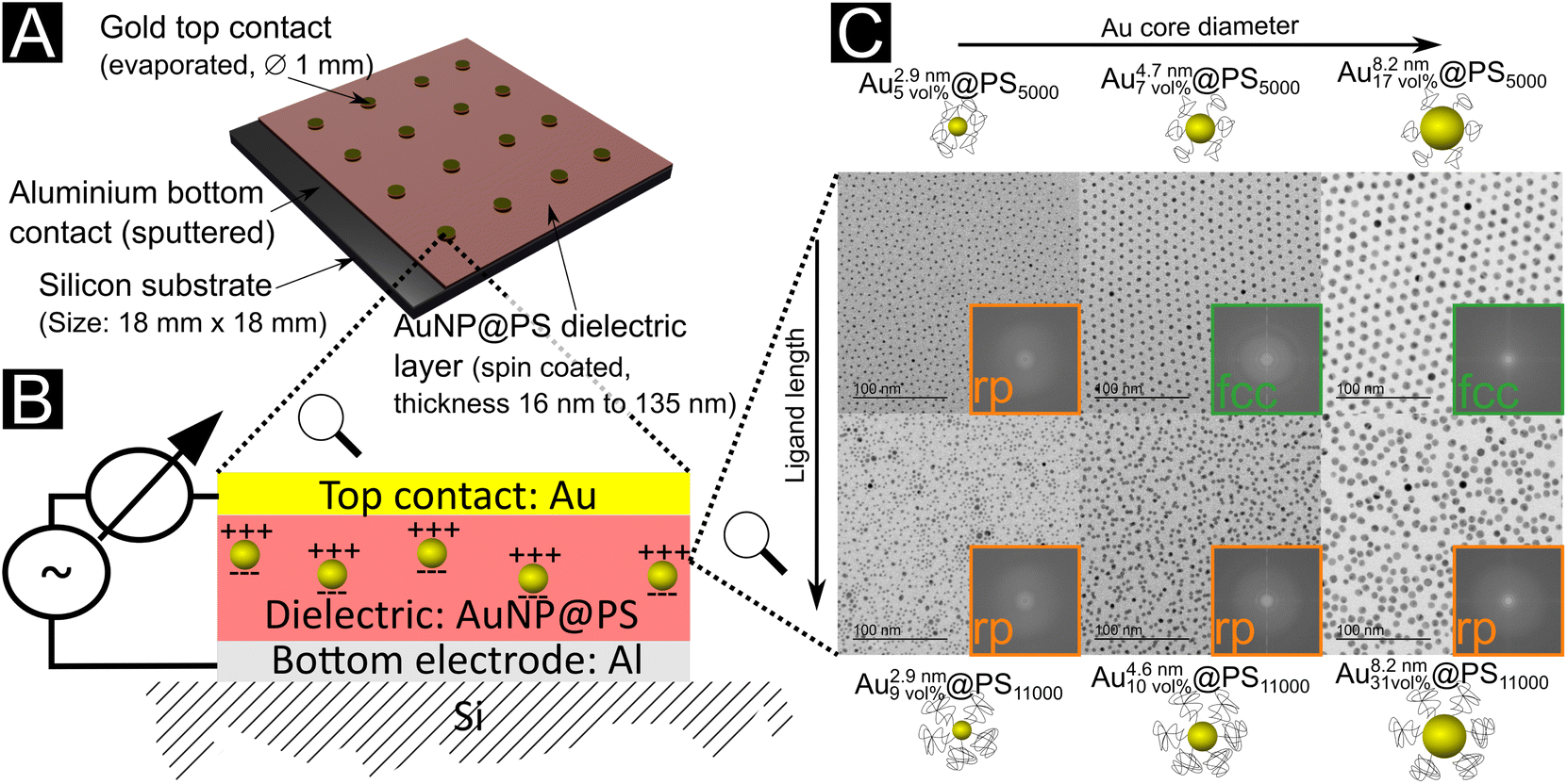 | ||
| Fig. 1 (A) Hybrid Au@PS nanodielectrics spin-coated on silicon substrates and contacted with evaporated metal electrodes to form capacitors. (B) Schematic structure of the nanodielectric film with its polarized metal particles. (C) Transmission electron micrographs of the self-assembled Au@PS superlattices in drop-casted films. Depending on the core and shell geometry, they formed random packings (rp, orange) or face-centered cubic (fcc, green) superlattices. | ||
The size distributions of the gold cores provide an initial insight into the nanodielectrics’ film structure. The synthesised cores (capped with oleylamine) had monomodal size distributions. After ligand exchange with thiol-terminated polystyrene, the 4.7 nm and 8.2 nm diameter particles maintained their size distributions according to SAXS and TEM (see the ESI† for details). This led to nanodielectrics with narrow monomodal gold core distributions. The distribution of the 2.9 nm diameter particles with long polymer ligands changed during ligand exchange, and the X-ray scattering intensity at low q-values increased. The increase was too low to be explained by agglomeration,33 and dynamic light scattering did not indicate an increased agglomerate content (see the ESI†). Electron microscopy indicated a broadened core diameter distribution of 2.9 nm cores for Au2.9\ nm7\ vol%@PS11000 (with a width of at least 13%) and the formation of a fraction of larger particles with diameters up to 8 nm during ligand exchange (Fig. S5 in the ESI†). Nanodielectrics with 2.9 nm cores and PS11000 ligands thus had wider bimodal core size distributions.
We investigated the structure of the polymer shells both in the dispersion and in the dry films. Ligand exchange (with any of the two polymers) increased the hydrodynamic diameters determined with dynamic light scattering (DLS) (Table S3 in the ESI†) by 5 nm to 6 nm for the 2.9 nm diameter cores and by 8 nm to 9 nm for the larger cores. The increase was slightly larger for PS5000 than for PS11000, indicating that PS5000 formed a shell with a larger number of ligands per area, while the longer polymer formed a sparser layer of collapsed polymers. Thermogravimetric analysis (see the ESI† for details) supported this hypothesis and indicated 3–4 times lower ligand areal densities for PS11000 than for PS5000. Apparently, the long polymers assume a collapsed “mushroom configuration” that reduces their areal density on a surface as previously reported.34
The areal density increased by 50% to 60% when decreasing the core diameter from 8.2 nm to 4.7 nm for both ligands, a known effect of increasing curvature.35 The areal density on 2.9 nm cores was 8% lower than for 4.7 nm cores with the same ligand. This unexpected decrease with increased curvature may be due to the strong faceting of 2.9 nm cores. Molecular dynamics simulations of alkanethiols on gold nanocrystals indicate that weaker bonds form between thiols and highly faceted spheres, reducing the areal density.36
2.1. Metal content and dielectric properties
Table 1 provides an overview of the dielectric properties of capacitors with different nanodielectrics. The exact gold contents of the dry nanodielectric films were quantified by thermogravimetric analysis of the reference samples and found to be in the range of 5 vol%–31 vol%. Details of the calculations and error estimations can be found in the ESI.† We calculated the permittivity from the measured capacities using a parallel plate capacitor model (eqn (4)). This neglects the roughness of the sputtered aluminum electrodes (Ra = 3.0 nm) and of the dielectric films (Ra = 1.1 nm), which is justified because they were far below the thickness of the dielectric layers in all cases (see the ESI†).δ were calculated and averaged from the dielectric spectrograms of at least 11 spin-coated and 12 inkjet-printed capacitors
| Sample label | Preparation method | t [nm] | C p [pF] | ε r [−] | tanδ [−] |
|---|---|---|---|---|---|
| Au2.9\ nm5\ vol%@PS5000 | Spin coated | 135.4 ± 7.1 | 165 ± 3 | 3.2 ± 0.2 | 0.010 ± 0.003 |
| Au2.9\ nm9\ vol%@PS11000 | Spin coated | 68.2 ± 2.3 | 688 ± 29 | 6.7 ± 0.4 | 0.307 ± 0.013 |
| Au4.7\ nm7\ vol%@PS5000 | Spin coated | 48.1 ± 3.0 | 490 ± 33 | 3.4 ± 0.2 | 0.029 ± 0.055 |
| Au4.6\ nm10\ vol%@PS11000 | Spin coated | 51.1 ± 1.4 | 654 ± 16 | 4.8 ± 0.1 | 0.068 ± 0.004 |
| Au8.2\ nm17\ vol%@PS5000 | Spin coated | 30.6 ± 0.9 | 1107 ± 55 | 4.9 ± 0.3 | 0.023 ± 0.003 |
| Au8.2\ nm31\ vol%@PS11000 | Spin coated | 15.7 ± 1.0 | 6039 ± 677 | 13.6 ± 1.6 | 0.093 ± 0.033 |
| Au4.6\ nm10\ vol%@PS11000 | Inkjet printed | ≈25 | 1316 ± 55 | n.a. | 0.071 ± 0.006 |
The dielectric constants and losses in the frequency range of 1 Hz to 1 × 10⁶ Hz are shown in Fig. 2a and b. The dielectric losses were minimal around 10 kHz, with dielectric constants that were larger for hybrid layers with PS11000 than PS5000 ligands at any given core diameter (Fig. 2c). The Au volume fractions were always larger for layers with PS11000 than for PS5000, and the dielectric constants rose with Au volume fraction. At low frequencies, the largest dielectric constant was 98.3 for Au2.9\ nm9\ vol%@PS11000 at 1 Hz; at 10 kHz it was 15 for Au8.2\ nm31\ vol%@PS11000. The plot in Fig. 2c includes dielectric constants from reference thin film capacitors with PS–SH dielectric layers and previously published data with different core sizes.10 The dielectric constant increased non-linearly with increasing Au volume fraction for all core sizes.
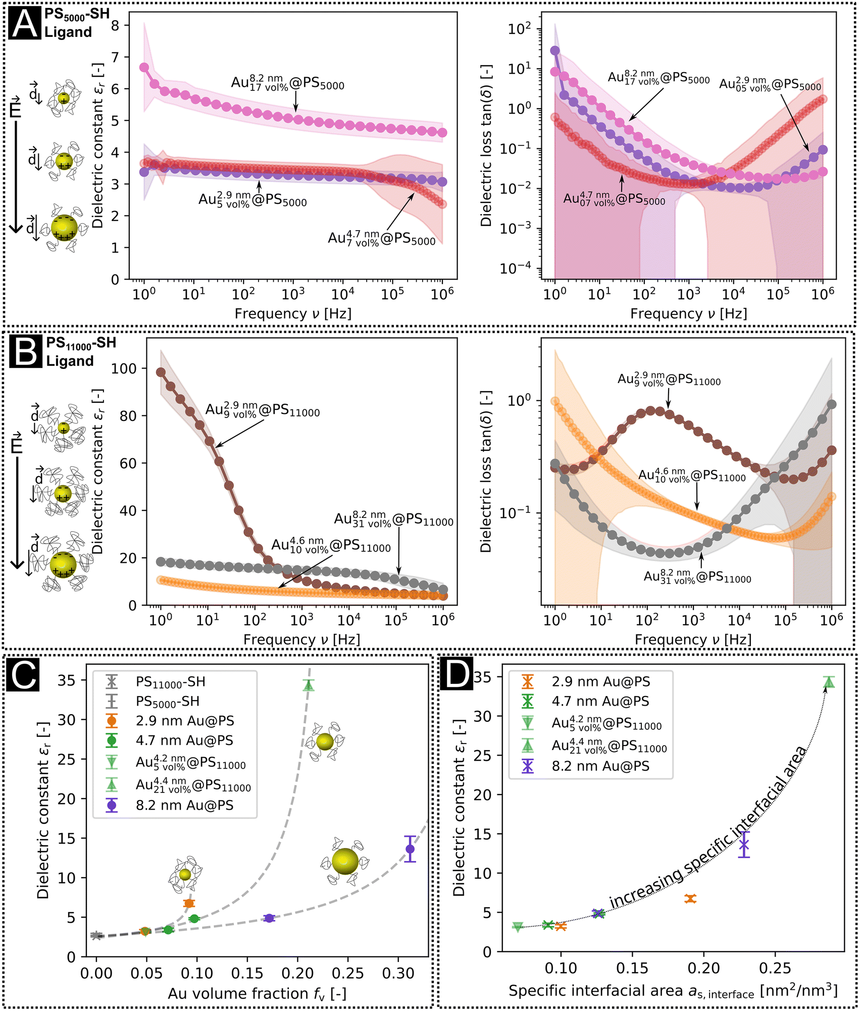 | ||
| Fig. 2 Dielectric constants and losses of Au@PS hybrids with (a) the PS5000 ligand and (b) with the PS11000 ligand. (c) Dielectric constants at 10 kHz as a function of gold volume fractions from TGA. Reference data for fv,Au = 0 were measured on pure PS11000–SH layers (see our previous publication10), and the dielectric constants for medium-sized particles with high and low ligand densities were taken from the values of the samples Audisordered0.05@PS and Audisordered0.21@PS from ref. 10. The dashed lines are fits to the percolation function as stated in eqn (1). (d) Dielectric constants at 10 kHz as a function of the calculated specific interfacial area in thin film capacitors with small, medium, and large AuNPs. | ||
The dielectric losses of nanodielectrics at their minima were smaller for PS5000 than for PS11000 (Fig. 2a and b). The denser PS5000 shells apparently decrease tunneling and leakage currents. Such trade-offs between high dielectric constants and low dielectric losses have been frequently described for type II composites, too.19–21,37–40
We previously introduced a resistor–capacitor network model as originally suggested by Efros and Shklovskii41 and Dubrov et al.42 for type III hybrid nanoelectrics.10 Capacitors are formed between individual Au particles with the polymer shell around the particles acting as the dielectric; the tunnelling barrier between the Au cores is represented by parallel resistors that define the leakage currents. The individually attached polymer shells of Au@PS hybrids prevent percolation and enable high metal filling ratios. The dashed lines in Fig. 2c represent a fit to the percolation function41,42
 | (1) |
The percolation exponent that we found for 8.2 nm particles was q = 1.2, close to the exponent q = 1 of a 3D-lattice41 and similar to the exponent found for the 4.7 nm particles (q = 1.3). The percolation thresholds fc for the 4.7 nm (fc = 0.24) and 8.2 nm (fc = 0.41) particles were clearly above fc = 0.16 predicted for perfect spheres32 and measured by Fredin et al. for aluminum nanoparticles (AlNPs) in polypropylene (PP).23 The exponent for 2.9 nm particles was q = 0.3, and the percolation threshold fc = 0.10, smaller than the expected values for both 3-D lattices and spheres. The deviation is probably due to polarization and relaxation effects not considered in the model.
We now focus on the dielectric effects of the metal core diameter that go beyond the metal volume fraction. The dielectric constant at 10 kHz was 6.7 for Au2.9\ nm9\ vol%@PS11000 with 2.9 nm cores at a volume fraction of 9 vol% but only 4.8 for Au4.6nm10 vol%@PS11000 with 4.6 nm cores at a volume fraction of 10 vol%, for example. Such strong non-linearities cannot be reconciled with the Efros–Shklovskii model.
The Maxwell–Wagner–Sillars (MWS) polarization of conductor–insulator interfaces is an important mechanism in heterogeneous dielectrics.3,43,44 Nanodielectrics have large interfaces with areas that scale with the square of the metal volume fraction. We calculated the specific interfacial areas of our nanodielectrics,
 | (2) |
Fig. 2d shows the measured dielectric constants at 10 kHz as a function of as,interface. The values for the dielectric constants at 10 kHz, the Au volume fractions, and the specific interfacial areas of Au@PS hybrids with varying core diameters are summarized in Table S5 of the ESI.† Strong non-linear correlations exist between the specific interfacial area and dielectric constants. We propose that the overall dielectric properties of our nanodielectrics are due to a combination of MWS polarization and bulk polarization that is modulated by the interactions between multiple polarized particles.
2.2. Dielectric losses
Fig. 2a and b show the dielectric losses of our Au@PS hybrid nanodielectrics. All samples except Au2.9\ nm9\ vol%@PS11000 had minimal dielectric losses of between 0.01 and 0.06 at frequencies between 1 kHz (Au4.7\ nm7\ vol%@PS5000) and 61 kHz (Au4.6\ nm10\ vol%@PS11000). The increase of dielectric losses towards 1 MHz and a concurrent decrease of the dielectric constant is consistent with MWS relaxation.Fredin et al. reported a comparable relaxation around 1 MHz for AlNP/PP composites24 with Al volume contents of up to 12.4 vol% and explained it with the existence of aggregates.23,24 They modeled the losses using the Wagner model of dielectric composites for conductive spheres in an insulating medium45 that was later extended by Sillars.46 These theories predict a maximal dielectric loss and a drop in the dielectric constant at a relaxation frequency that is set by the shape of the filler particles, typically in the MHz range. Conductive particles in close proximity, for example in aggregates, can behave as single “joint particles”,24 too.
Our samples did not contain aggregates in the dispersion according to DLS. However, the Au2.9\ nm9\ vol%@PS11000 sample did contain a fraction of larger particles after ligand exchange (see above and Fig. S5b in the ESI†). The Wagner model of polarization45 and its extension by Sillars46 predict an increase of interfacial polarization and a decrease of the frequency for dielectric losses with increasing particle diameter. This is consistent with the local maximum in the dielectric loss connected with a strong decrease of the dielectric constant around the frequency 100 Hz for the Au2.9\ nm9\ vol%@PS11000 sample. No local maximum of the dielectric loss was observed for the other samples within the measured frequency range.
Matavž et al. argued that limited conduction of the electrodes can cause an additional decrease of the dielectric constant connected with an increase of the dielectric loss at high frequencies.8 Our sputtered Al bottom electrodes had considerable contact resistivities of Rp = 5 Ω to 100 Ω according to impedance measurements. They are likely responsible for the dielectric losses of 0.3 at high frequencies that increase to 30 when shifting to 1 Hz that we observed for all core sizes. These losses were not connected with a decrease of the dielectric constant and are probably not due to MWS polarization.
2.3. Dielectric strength
The maximal field strength that the nanodielectric can sustain without breakdown—its “dielectric strength”—is an important parameter for devices because it limits the energy stored per volume. The dielectric strength of our Au@PS hybrids was measured by slowly increasing the DC bias until a non-linear current increase indicated the breakdown voltage Vbd (see Fig. S9 in the ESI†). The breakdown strengths Ebd (average of two measurements) were in the range of 71.1 MV m−1 to 158.7 MV m−1 (see Fig. 3b and Table S6 in the ESI†). We did not find any sign of decreased breakdown strength at larger Au volume fractions. The covalently attached PS shells apparently ensured electric insulation even for the largest 8.2 nm particles with Au volume fractions of up to 31 vol%. | ||
| Fig. 3 Particle packing and dielectric breakdown strength of Au@PS hybrids. (a) Drop-casted particles with fast Fourier transform (FFT) (top) and the cross section of a thin film capacitor (bottom) of Au4.7\ nm7\ vol%@PS5000 as an example for a sample with face-centered-cubic particle packing. (b) Dielectric breakthrough strengths of Au@PS hybrids. Layers with random packing are shown in green, and layers with face-centered-cubic (fcc) packing are shown in orange. (c) Drop-casted particles with FFT (top) and the cross section of a thin film capacitor (bottom) of Au2.9\ nm9\ vol%@PS11000 as an example for a sample with randomly packed particles. | ||
We prepared drop-casted layers from 2.9 nm to 8.2 nm diameter core particles on Kapton foil and analyzed their structure by SAXS in transmission mode (Fig. S6 in the ESI†) and TEM (Fig. 1c). Cross sections of spin-coated layers were prepared with a focus ion beam and investigated using TEM (Fig. 3a and c for examples and Fig. S8 in the ESI†). Only layers made form Au4.7\ nm7\ vol%@PS5000 and Au8.2\ nm17\ vol%@PS5000 showed regular fcc packings. All other nanodielectrics were composed of random particle arrangements. Small gold cores were the only to form layers with random packing for PS5000 ligands (Au2.9\ nm5\ vol%@PS5000). We believe that the high curvature of these cores resulted in a comparatively low ligand density of PS5000. The sparse shells have heterogeneous structures that cause complex anisotropic geometries and interactions between neighboring particles, which impedes the order (see the ESI† for a detailed discussion). The van der Waals interaction between cores is too weak to create a clear free energy minimum for the crystalline superlattice, leading to randomly packed films.
The two samples with the largest dielectric breakdown strength (by a factor of at least 1.6) had regular fcc packing. It is conceivable that the regular particle spacings in supercrystals reduce locally enhanced fields that provoke dielectric breakdown. The structure factors from SAXS in Fig. S7 (see analysis in the ESI†) imply that some particles in randomly packed particles had surface-to-surface distances of only 0.1 nm (Au8.2\ nm31\ vol%@PS11000), while fcc packing assured inter-particle spacings of at least 2.5 nm (Au4.7\ nm7\ vol%@PS5000). Regular particle spacing reduces the probability of random conductive pathways that can cause losses and dielectric breakdown, e.g., via tunneling. Fig. 1c illustrates that some metallic cores are more likely to be close to each other in the randomly packed layers than in the fcc layers. Nanoscale pinholes can be at the origin of dielectric breakdown, too; they may form during processing of the films due to the evaporation of the solvent. Both the fcc packed samples had comparable breakdown voltages despite the different core diameters of 4.7 nm and 8.2 nm. The large surface-to-surface distances for these samples may obscure the effect of core diameter. Nanodielectrics of randomly packed particles with shorter polymers consistently had larger breakdown strengths that exceeded 100 MV m−1, while those with long polymers remained below 71 MV m−1. It is likely that the density and thickness of the ligand shell affect both particle packing and breakdown strength. The homogeneous ligand shells with a high areal ligand density formed by PS5000 aided self-assembly and prevented dielectric breakdown. Even in the case of Au2.9\ nm5\ vol%@PS5000, where particle packing was disordered, the large areal ligand density increased the breakdown strength over particles with the long polymer (see Table S2 in the ESI† for details).
2.4. Inkjet printed dielectric layers on flexible PET substrates
The nanodielectrics discussed here are particularly suitable for inkjet printing. Nanoscale particles fit through the nozzles of an inkjet printing cartridge. Their polymer shells provide efficient stabilization and prevent agglomeration that would lead to blockage of the nozzles. The viscosity of covalently bound hybrid polymer–particle dispersions is lower than that of polymer solutions at the same concentration. We, therefore, were able to print a dispersion of Au4.6\ nm10\ vol%@PS11000 as dielectric layers on aluminum coated PET substrates using a standard piezo-driven inkjet printer. Evaporated gold top contacts with diameters of 1 mm formed thin film capacitors. Fig. 4b shows a surface profile from white light interferometry (WLI) of the dried ink droplets with a surface roughness of Ra = 110.9 nm over an area of 700 μm × 530 μm (see the ESI† for comparison with spin-coated samples). The top layer has a texture that is due to the print head moving in the y-direction that is clearly seen.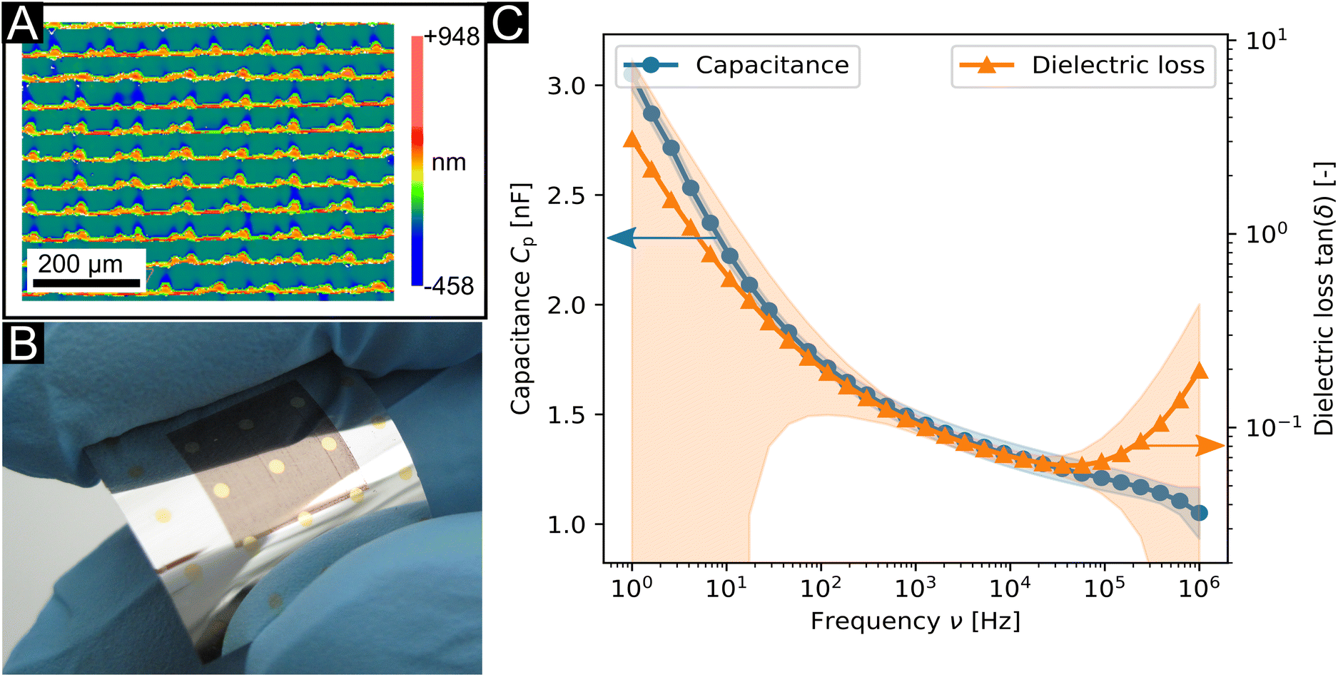 | ||
| Fig. 4 Inkjet printed flexible thin film capacitors on an aluminium coated PET substrate based on Au4.6\ nm10\ vol%@PS11000. (A) Surface profile of a film printed in two passes at 500 DPI from WLI. (B) Photograph and (C) dielectric properties of flexible thin film capacitors. | ||
The average capacitance of the flexible thin film capacitors was (1.30 ± 0.06) nF for an area of 0.79 mm2 with a dielectric loss of 0.071 ± 0.006 at 10 kHz. Both values were increasing towards higher frequencies, similar to those of the spin-coated samples. The thicknesses of the dielectric layers were estimated by comparison of the dielectric constant to the spin coated-samples to be ≈25 nm.
Mechanical flexibility was tested by bending a printed sample on a support to a radius of ≈8 mm in a bending machine (see Fig. S10b in the ESI†) over 3500 bending cycles. The capacitors maintained their functionality after these bending cycles; the changes in dielectric properties were below 8% (details discussed in the ESI†).
3. Conclusions
We investigated the effect of the nanoscale structure on the properties of Au@PS hybrid nanodielectrics. Gold cores with diameters of 2.9 nm, 4.7 nm, and 8.2 nm were synthesized, covalently grafted with two different polystyrene shells, and deposited as dielectric layers using spin-coating and inkjet printing. We found that the density and thickness of the shells depended on the Au core size. Long polymers formed mushroom coils that led to reduced areal densities.The dielectric constants of the films increased with decreasing core sizes for comparable Au volume fractions. For example, films of Au2.9\ nm9\ vol%@PS11000 had 40% larger dielectric constants than Au4.6\ nm10\ vol%@PS11000 at 10 vol% Au. We rationalized this scaling using a model that combines a resistor–capacitor network with Maxwell–Wagner–Sillars (MWS) polarization. Qualitatively, a decrease of core sizes at constant Au volume fractions led to an increase in the number of microcapacitors in the hybrid. Increasing specific interfacial areas increased dielectric constants beyond the volumetric contribution of the metal. Interfacial polarization dominates the dielectric constants.
The dielectric breakdown strengths of the Au@PS hybrids were in the range of 71.1 MV m−1 to 158.7 MV m−1. Particle packing affected the breakdown strength. The highest breakdown strengths were found for Au4.7\ nm7\ vol%@PS11000 and Au8.2\ nm17\ vol%@PS5000, where ordered particle packing reduced the local enhancement of the electric field between nearby particles. Randomly packed Au2.9\ nm5\ vol%@PS5000 films of 2.9 nm particles with comparatively high ligand areal densities of 1.2 nm−2 had higher breakdown strengths.
Flexible thin film capacitors were formed by inkjet printing nanodielectrics on aluminum coated PET foils using Au4.6\ nm10\ vol%@PS11000 particles. Those had capacitances of 1.30 ± 0.06 nF over 0.79 mm2 and were stable after 3500 bending cycles over a radius of ≈8 mm. This makes them suitable for dielectric layers in printed flexible electronics.
4. Materials and methods
4.1. Materials
All chemicals were used without purification as received from the supplier and, unless stated otherwise, obtained from Sigma Aldrich, Germany, among them thiol-functionalized polystyrene with molecular weights of Mn = 5000 Da and Mn = 11000 Da (both with polydispersity index ≤1.1).
4.2. Nanoparticle synthesis
Gold nanoparticles (Au NPs) with oleylamine (OAm) shells (Au@OAm) were synthesized following a modified synthesis protocol of Wu et al.47 as previously reported.10 For the synthesis of a typical batch of Au@OAm NPs, a mixture of 20 mL of filtered OAm (ACROS Organics, Germany, C18 content 80% to 90%) and 20 mL of the solvent (n-pentane (99% purity) for 2.9 nm Au cores, n-hexane (abcr GmbH, Germany, 99% purity) for 4.7 nm Au cores, and benzene (99% purity) for 7.0 nm Au cores) was prepared. 200 mg of HAuCl4·3H2O (ACROS Organics, Germany) were dissolved in 32 mL of the OAm–solvent mixture. The solution turned immediately red and was stirred at room temperature for the times of 90 min for the 2.9 nm sized Au cores, 20 min for 4.7 nm sized Au cores, and 45 s for 7.0 nm sized Au cores. Then, a solution of 100 mg of tetrabutylammonium bromide in the remaining 8 mL of the OAm–solvent mixture was added. The solution turned dark blue and was stirred further for about 1 h at room temperature.Purification was performed by adding 50 mL of ethanol and 10 mL of methanol to 40 mL of the as-prepared Au@OAm NP dispersion and the mixture assumed a blue tinge due to particle agglomeration. It was distributed into two centrifuge tubes of 50 mL and centrifuged (Rotanta 460 RS, Hettich, Germany, 1550 rcf, t = 5 min). Then, the clear supernatant was decanted and the NPs were redispersed in 40 mL of cyclohexane (Roth, Germany, 99.9% purity). The resulting particle dispersion was again mixed with 40 mL of ethanol and 20 mL of methanol, and the cycle was repeated. Finally, the Au@OAm NPs were redispersed in 40 mL of the final solvent toluene (Roth, Germany, 99.8% purity).
Particles with 8.2 nm diameter were prepared by overgrowing the 7.0 nm particles from above. 40 mL of the washed 7.0 nm AuNP@OAm dispersed in toluene were stirred on a hot plate at 63 °C. A mixture of 2 mL of filtered OAm and 2 mL of toluene was prepared. 100 mg of HAuCl4·3H2O (ACROS Organics, Germany) were fast dissolved in the OAm–toluene mixture by vigorous shaking and immediately added to the AuNP@OAm dispersion. The stirring was continued for about 24 h at 63 °C. Purification was performed as stated above, except the centrifuge was set to 5230 rcf for t = 20 min in the second centrifugation cycle. The overgrown 8.2 nm Au@OAm particles were redispersed in 40 mL of the final solvent toluene.
Thiol-functionalized PS (PS–SH) was attached to the Au NPs following the grafting-to approach of Corbierre et al.48 and as described before.10 Briefly, the respective amount of PS–SH was weighted for a batch of Au@OAm NPs made of 200 mg gold acid depending on the core size: for AuNPs capped with PS5000–SH (Mn = 5000 Da), the respective amounts of the polymer were 480 mg for 2.9 nm sized Au cores, 350 mg for 4.7 nm sized Au cores, and 236 mg for 8.2 nm sized Au cores; for AuNPs capped with PS11000–SH (Mn = 11000 Dalton), the respective amounts of the polymer were 500 mg for 2.9 nm sized Au cores, 390 mg for 4.7 nm sized Au cores, and 237 mg for 8.2 nm sized Au cores. This respective amount of the polymer was dissolved in 6 mL of toluene with the aid of 3 min ultrasonication. The PS–SH solution was added to the Au@OAm NP dispersion and stirred on a hot plate at 60 °C for one week. To purify the dispersions, they were centrifuged in an ultracentrifuge (Optima XE-90, Beckman Coulter, USA) with a SW 32 Ti rotor (174900 rcf, t = 165 min, 25 °C) for the 4.7 nm and 8.2 nm sized Au cores and with a SW 60 Ti rotor (485000 rcf, t = 210 min, 25 °C) for the 2.9 nm sized Au cores. The light supernatant was removed with a pipette and the Au@PS NPs were dispersed in toluene at the desired concentration with the aid of an ultrasonic bath. The gold concentrations of the final dispersions were quantified by measuring optical absorption at 400 nm.49
4.3. Thermogravimetric analysis
The gold and polystyrene contents of AuNP@PS were quantified by drying approximately 250 μL of the respective dispersion in a TGA crucible on a hot plate at 60 °C and additional drying in a vacuum oven at 30 °C overnight. The solid samples (6 mg to 9 mg dry mass) were heated to 1000 °C in a Netzsch STA 449 F3 TGA (Netzsch, Germany) under Ar at a heating rate of 10 K min−1. At 1000 °C, the furnace gas was switched to O2 and held for 10 min for complete oxidation of the organic part.For each prepared ink, two measurements were performed; we report the mean value of the final residual mass of elemental Au as explained in the ESI.†
4.4. Dielectric layer preparation
We prepared smooth dielectric layers on silicon 〈100〉 wafers (Siegert Wafer, Germany) with an intrinsic SiO2 layer that we had coated with aluminum layers (thickness (60 ± 14) nm) through magnetron sputtering. We cleaved these rigid substrates into square pieces of 18 mm × 18 mm. The liquid ink was dispensed onto the pieces and they were accelerated to ω = 1000 rpm with for 60 s to form homogeneous films. At one edge of the sample, a metallic bottom contact was formed by removing the dielectric coating with a toluene-soaked cotton bud. Residual solvent in the spin-coated samples was evaporated overnight in a vacuum oven at 25 °C. We used a shadow mask to evaporate the Au circular top contacts of diameter 1 mm and thickness (157 ± 4) nm on the sample. Hence, at one sample there were 9 to 16 thin film capacitors prepared which could be contacted for dielectric measurement.
We measured the thickness of the spin-coated AuNP@PS layers on the reference samples spin-coated on glass microscope cover slips. We prepared a cross-like scratch to create a step that we then measured using a white light interferometer (Zygo New View 5000 and Zygo New View 7300, Zygo Corporation, USA) with a filtered white light source (tungsten halogen lamp) and using the MetroPro software (Zygo Corporation, USA).
4.5. Inkjet printing
We prepared flexible capacitors with inkjet printed dielectric layers on polyethylene terephthalate (PET) foil (Melinex ST504, Pütz Folien, Germany) that were covered with a sputtered aluminum layer on the non-pre-treated side of the foil as explained above for the rigid substrates. Square pieces of 18 mm × 18 mm were cut and cleaned as described above. Dispersions based on 4.7 nm Au@PS11000 particles in toluene that were also used for spin-coating were used for printing (see above for synthesis).We filled the respective ink in the cartridges of a PIXDRO LP50 inkjet printer (SÜSS MicroTec SE, Germany) mounted on a piezo print head (DMC-11610, Dimatix, USA) with a nozzle diameter of 21.5 μm. We used a single nozzle for printing, where the piezo actuator was driven with a pulse shape waveform (holding voltage 8 V, pulse voltage 29 V) at a pulse length of 9 μs and an ejection frequency of 1000 Hz. We applied a negative pressure of −1 mbar to the ink vessel in order to stabilize droplet formation. The printing was performed in a temperature and humidity-controlled laboratory (22 °C with 50% relative humidity). A camera and a stroboscope allowed the observation of droplet formation before printing.
We printed squares of 10 mm × 10 mm with two passes at a droplet density of 500 DPI on an aluminum coated PET foil, where the first pass was orthogonal to the second. We ensured the complete evaporation of the solvent by drying in a vacuum oven at 25 °C and ∼50 mbar over night. We used thermal evaporation to deposit gold top contacts with circular shapes and diameters of 1 mm as described above for the rigid spin-coated samples.
4.6. Transmission electron microscopy
Individual AuNP@PS nanoparticles were imaged using a JEM-2011 LaB6 TEM and a JEM-2100 LaB6 TEM (JOEL, Germany), both with high-resolution pole pieces at 200 kV acceleration voltage, and bright field electron micrographs were obtained with an Orius SC1000 CCD camera (Gatan, USA). We prepared samples by diluting the AuNP@PS inks with toluene and dropping on a carbon TEM grid. In order to identify the order in the AuNP arrangement, fast Fourier transform (FFT) of the binary TEM images (using an auto threshold filter) was performed with the Fiji software.We prepared cross sections of thin film capacitors by covering the samples with a conducting carbon layer (to prevent charging of the samples) and two protecting platinum layers via electron and ion beam deposition. Then, we cut thin lamellae using a focused ion beam (FIB) of a combined FIB/SEM – a dual beam scanning microscope (Versa 3D Low Vac, FEI Company, USA). For fast cutting, the ion current was 7 nA; for fine cutting, the ion current was 0.3 nA with a beam spot diameter of 0.8 nm. The FIB lamellae were connected to an Omniprobe nanomanipulator, mounted on a TEM sample holder, and analyzed using TEM (see above for the instrument).
4.7. Dynamic light scattering
The dynamic light scattering measurements were performed on diluted inks with an ALV/CGS-3 goniometer system (ALV GmbH, Germany) using a laser wavelength λ of 632.8 nm, acquisition times of 180 s (600 s for the 2.9 nm Au cores), and scattering angles θ between 30° and 150° in steps of 10°. Plotting of the inverse correlation times τ−1vs. the square of the wavenumbers q2 that were calculated at each scattering angle as (n is the refractive index of the solvent toluene)50 resulted the translational diffusion coefficient Dtrans as the slope of the plot.51Dtrans was transferred to the hydrodynamic diameter using the Stokes–Einstein relationship:51,52
 | (3) |
4.8. Small angle X-ray scattering
We recorded small angle X-ray scattering (SAXS) patterns from the AuNP@PS dispersion and drop-casted films in a Xenocs Xeuss 2.0 laboratory set-up. X-rays at the copper Kα-line with a wavelength of λ = 0.154 nm were provided by a Genix 3D source (Xenocs SAS, France). Scattered intensities were detected using a Dectris Pilatus 3R 1 M detector (DECTRIS, USA) of scattering vectors q = 4πλ−1sinθ between 0.1 nm−1 and 10 nm−1, with the scattering angle 2θ.
All synthesized Au@OAm and Au@PS NPs were analyzed in transmission SAXS experiments using borosilicate capillaries sealed by epoxy (see Fig. S4 in the ESI†). The spectra were azimuthally integrated with the Foxtrot software (Soleil, France), pure solvent scattering was subtracted as the background from the data, and the spectra were fitted by a polydisperse spherical form factor model using a Schulz–Zimm distribution to obtain the average particle diameter dcore and the width of the particle size distribution σ with the SASfit software (Paul Scherrer Institute, Switzerland55).
We prepared films of AuNP@PS for SAXS by drop-casting particle dispersions on Kapton foil and evaporation at room temperature. Transmission SAXS was recorded as above, the Kapton foil's scattering from reference measurements was subtracted, and the spectra were evaluated by means of an effective structure factor. Details are provided in the ESI.†
4.9. Dielectric spectroscopy
Impedance spectrometry using an Alpha Analyzer spectrometer (Novocontrol Technologies, Germany) in the frequency range of 1 × 10⁶ Hz to 1 Hz at room temperature with a voltage amplitude of 50 mV was employed to characterize the AuNP@PS thin film capacitors. The bottom and top contacts of the samples were contacted to the ZG4 test interface of the alpha analyzer via contact pins mounted on micro manipulators during the measurements; the resistance of the Al bottom contacts was determined by coming in contact with both contact pins on the Al bottom electrode in a short circuit. A parallel equivalent circuit model was used to determine the capacitance in parallel Cp, the resistance in parallel Rp, and the dielectric loss tanδ from the measured data using the WinDETA software (Novocontrol Technologies, Germany). Several thin film capacitors were measured per layer type. If the analysis did not indicate dielectric behavior (e.g., because of the dielectric losses tanδ way above 1), we assumed damage such as pin holes and discarded the sample. The yield of the functional samples ranged between 40% (for 15 measured thin film capacitors) and 86% (for 28 measured thin film capacitors) for the spin-coated samples and was 80% (for 15 measured thin film capacitors) for the flexible inkjet printed sample.
The dielectric constant εr was extracted from the capacitance in parallel Cp, which was measured during the impedance spectroscopy experiment using the following equation:
 | (4) |
δ.
Author contributions
Roman Buchheit: methodology, investigation, formal analysis, and writing – original draft. Bart-Jan Niebuur: investigation and formal analysis (SAXS data). Lola González-García: supervision and writing – review and editing. Tobias Kraus: conceptualization, funding acquisition, resources, supervision, and writing – review and editing.Conflicts of interest
There are no conflicts to declare.Acknowledgements
The authors thank Dr. Marcus Koch and Birgit Nothdurft for performing the FIB cuts and recording the TEM images for this work, Robert Drumm for performing the TGA measurements, Prof. Dr. Roland Bennewitz and co-workers for the AFM measurements, and Robert Strahl for his support with inkjet printing. We thank the workshop of INM for manufacturing some elements of the dielectric measurement setup. We thank the chair of functional materials of Prof. Dr.-Ing. Frank Mücklich for the access to the white light interferometer.References
- J. Wiklund, A. Karakoç, T. Palko, H. Yiğitler, K. Ruttik, R. Jäntti and J. Paltakari, J. Manuf. Mater. Process., 2021, 5, 89 CAS.
- W. Chang Ee and K. Yew Cheong, Phys. B, 2008, 403, 611–615 CrossRef.
- E. Ivers-Tiffée and W. von Münch, Werkstoffe der Elektrotechnik: Mit 40 Tabellen, Teubner, Wiesbaden, 10th edn, 2007 Search PubMed.
- Y.-G. Ha, K. Everaerts, M. C. Hersam and T. J. Marks, Acc. Chem. Res., 2014, 47, 1019–1028 CrossRef CAS PubMed.
- F. Zhang, C. Tuck, R. Hague, Y. He, E. Saleh, Y. Li, C. Sturgess and R. Wildman, J. Appl. Polym. Sci., 2016, 133, 43361 Search PubMed.
- A. Mohapatra, S. K. Tuli, K.-Y. Liu, T. Fujiwara, R. W. Hewitt Jr., F. Andrasik and B. I. Morshed, 2018 40th Annual International Conference of the IEEE Engineering in Medicine and Biology Society (EMBC), Piscataway, NJ, 2018, pp. 4277–4280.
- T. Kaydanova, A. Miedaner, J. D. Perkins, C. Curtis, J. L. Alleman and D. S. Ginley, Thin Solid Films, 2007, 515, 3820–3824 CrossRef CAS.
- A. Matavž, B. Malič and V. Bobnar, J. Appl. Phys., 2017, 122, 214102 CrossRef.
- G. McKerricher, R. Maller, V. Mohammad, M. A. McLachlan and A. Shamim, Ceram. Int., 2017, 43, 9846–9853 CrossRef CAS.
- R. Buchheit, B. Kuttich, L. González-García and T. Kraus, Adv. Mater., 2021, 33, 2103087 CrossRef CAS PubMed.
- B. J. Kang, C. K. Lee and J. H. Oh, Microelectron. Eng., 2012, 97, 251–254 CrossRef CAS.
- J. Lim, J. Kim, Y. J. Yoon, H. Kim, H. G. Yoon, S.-N. Lee and J. Kim, Curr. Appl. Phys., 2012, 12, e14–e17 CrossRef.
- M. Mikolajek, A. Friederich, C. Kohler, M. Rosen, A. Rathjen, K. Krüger and J. R. Binder, Adv. Eng. Mater., 2015, 17, 1294–1301 CrossRef CAS.
- M. Mikolajek, T. Reinheimer, N. Bohn, C. Kohler, M. J. Hoffmann and J. R. Binder, Sci. Rep., 2019, 9, 13324 CrossRef PubMed.
- T. Reinheimer, R. Azmi and J. R. Binder, ACS Appl. Mater. Interfaces, 2020, 12, 2974–2982 CrossRef CAS PubMed.
- J. Y. Li, L. Zhang and S. Ducharme, Appl. Phys. Lett., 2007, 90, 132901 CrossRef.
- Z.-M. Dang, J.-K. Yuan, J.-W. Zha, T. Zhou, S.-T. Li and G.-H. Hu, Prog. Mater. Sci., 2012, 57, 660–723 CrossRef CAS.
- L. Qi, B. I. Lee, S. Chen, W. D. Samuels and G. J. Exarhos, Adv. Mater., 2005, 17, 1777–1781 CrossRef CAS.
- Y. Shen, Y. Lin, M. Li and C.-W. Nan, Adv. Mater., 2007, 19, 1418–1422 CrossRef CAS.
- A. Toor, H. So and A. P. Pisano, Appl. Surf. Sci., 2017, 414, 373–379 CrossRef CAS.
- A. Toor, H. So and A. P. Pisano, ACS Appl. Mater. Interfaces, 2017, 9, 6369–6375 CrossRef CAS PubMed.
- C.-W. Nan, Y. Shen and J. Ma, Annu. Rev. Mater. Res., 2010, 40, 131–151 CrossRef CAS.
- L. A. Fredin, Z. Li, M. T. Lanagan, M. A. Ratner and T. J. Marks, Adv. Funct. Mater., 2013, 23, 3560–3569 CrossRef CAS.
- L. A. Fredin, Z. Li, M. T. Lanagan, M. A. Ratner and T. J. Marks, ACS Nano, 2013, 7, 396–407 CrossRef CAS PubMed.
- S. Naderi, J. P. Heath and J. S. Dean, Ceram. Int., 2019, 45, 361–368 CrossRef CAS.
- A. Teverovsky, IEEE Trans. Dielectr. Electr. Insul., 2012, 19, 1448–1455 CAS.
- M. H. Garner, H. Li, Y. Chen, T. A. Su, Z. Shangguan, D. W. Paley, T. Liu, F. Ng, H. Li, S. Xiao, C. Nuckolls, L. Venkataraman and G. C. Solomon, Nature, 2018, 558, 415–419 CrossRef CAS PubMed.
- M. H. Garner, H. Li, M. Neupane, Q. Zou, T. Liu, T. A. Su, Z. Shangguan, D. W. Paley, F. Ng, S. Xiao, C. Nuckolls, L. Venkataraman and G. C. Solomon, J. Am. Chem. Soc., 2019, 141, 15471–15476 CrossRef CAS PubMed.
- Y. Zhang, X. Qiu, P. Gordiichuk, S. Soni, T. L. Krijger, A. Herrmann and R. C. Chiechi, J. Phys. Chem. C, 2017, 121, 14920–14928 CrossRef CAS PubMed.
- G. D. Kong, H. Song, S. Yoon, H. Kang, R. Chang and H. J. Yoon, Nano Lett., 2021, 21, 3162–3169 CrossRef CAS PubMed.
- G. D. Kong, S. E. Byeon, J. Jang, J. W. Kim and H. J. Yoon, J. Am. Chem. Soc., 2022, 144, 7966–7971 CrossRef CAS PubMed.
- Z.-M. Dang, J.-K. Yuan, S.-H. Yao and R.-J. Liao, Adv. Mater., 2013, 25, 6334–6365 CrossRef CAS PubMed.
- J. Sindram, M. Krüsmann, M. Otten, T. Pauly, L. Nagel-Steger and M. Karg, J. Phys. Chem. B, 2021, 125, 8225–8237 CrossRef CAS PubMed.
- D. Dukes, Y. Li, S. Lewis, B. Benicewicz, L. Schadler and S. K. Kumar, Macromolecules, 2010, 43, 1564–1570 CrossRef CAS.
- K. Rahme, L. Chen, R. G. Hobbs, M. A. Morris, C. O'Driscoll and J. D. Holmes, RSC Adv., 2013, 3, 6085–6094 RSC.
- T. Djebaili, J. Richardi, S. Abel and M. Marchi, J. Phys. Chem. C, 2013, 117, 17791–17800 CrossRef CAS.
- Z.-M. Dang, Y. Shen and C.-W. Nan, Appl. Phys. Lett., 2002, 81, 4814–4816 CrossRef CAS.
- Z.-M. Dang, Y.-H. Zhang and S.-C. Tjong, Synth. Met., 2004, 146, 79–84 CrossRef CAS.
- L. Fernández-García, M. Suárez, J. L. Menéndez, C. Pecharromán, R. Menéndez and R. Santamaría, Nanoscale Res. Lett., 2015, 10, 216 CrossRef PubMed.
- P. N. Vakil, F. Muhammed, D. Hardy, T. J. Dickens, S. Ramakrishnan and G. F. Strouse, ACS Omega, 2018, 3, 12813–12823 CrossRef CAS PubMed.
- A. L. Efros and B. I. Shklovskii, Phys. Status Solidi B, 1976, 76, 475–485 CrossRef CAS.
- V. E. Dubrov, M. E. Levinshtein and M. S. Shur, Sov. Phys. JETP, 1976, 43, 1050–1056 Search PubMed.
- P. A. M. Steeman and J. van Turnhout, Broadband Dielectric Spectroscopy, Springer, Berlin, Heidelberg, 2003, pp. 495–522 Search PubMed.
- C. Chanmal and J. Jog, Characterization Techniques for Polymer Nanocomposites, Wiley-VCH, s.l., 2012, pp. 167–184 Search PubMed.
- K. W. Wagner, Arch. Elektrotech., 1914, 2, 371–387 CrossRef.
- R. W. Sillars, Institution of Electrical Engineers - Proceedings of the Wireless Section of the Institution, 1937, vol. 12, pp. 139–155(16) Search PubMed.
- B.-H. Wu, H.-Y. Yang, H.-Q. Huang, G.-X. Chen and N.-F. Zheng, Chin. Chem. Lett., 2013, 24, 457–462 CrossRef CAS.
- M. K. Corbierre, N. S. Cameron and R. B. Lennox, Langmuir, 2004, 20, 2867–2873 CrossRef CAS PubMed.
- T. Hendel, M. Wuithschick, F. Kettemann, A. Birnbaum, K. Rademann and J. Polte, Anal. Chem., 2014, 86, 11115–11124 CrossRef CAS PubMed.
- B. J. Berne and R. Pecora, Dynamic Light Scattering: With Applications to Chemistry, Biology, and Physics, Dover Publications, Newburyport, 2013 Search PubMed.
- P. A. Hassan, S. Rana and G. Verma, Langmuir, 2015, 31, 3–12 CrossRef CAS PubMed.
- P. Atkins and J. de Paula, Physical Chemistry, Oxford University Press, New York, 9th edn, 2010 Search PubMed.
- M. D. Lechner Refractive Indices of Inorganic, Organometallic, and Organononmetallic Liquids, and Binary Liquid Mixtures, Springer, Berlin, Heidelberg, 1996, vol. 38A Search PubMed.
- C. Wohlfarth, Supplement to IV/18, Springer, Berlin, Heidelberg, 2009, vol. 25, pp. 447–458 Search PubMed.
- I. Breßler, J. Kohlbrecher and A. F. Thünemann, J. Appl. Crystallogr., 2015, 48, 1587–1598 CrossRef PubMed.
Footnote |
| † Electronic supplementary information (ESI) available. See DOI: https://doi.org/10.1039/d3nr01038d |
| This journal is © The Royal Society of Chemistry 2023 |