
 Open Access Article
 This Open Access Article is licensed under a Creative Commons Attribution-Non Commercial 3.0 Unported Licence
Quantum plasmonic two-dimensional WS2–MoS2 heterojunction†
Sharad
Ambardar
a,
Zachary H.
Withers
b,
Jiru
Liu
c,
Xiaoyi
Lai
d,
Abdullah
Albagami
ef,
Alina
Zhukova
f,
Pedro
Fabris Capelli
f,
Prasana K.
Sahoo
g and
Dmitri V.
Voronine
 af
af
aDepartment of Medical Engineering, University of South Florida, Tampa, FL 33620, USA. E-mail: dmitri.voronine@gmail.com
bDepartment of Physics, Stony Brook University, Stony Brook, NY 11790, USA
cDepartment of Physics, Texas A&M University, College Station, TX 77840, USA
dCAS Center for Excellence and Synergetic Innovation Center in Quantum Information and Quantum Physics, University of Science and Technology of China, Hefei, Anhui 230026, China
eDepartment of Physics, King Saud University, Riyadh 11362, Kingdom of Saudi Arabia
fDepartment of Physics, University of South Florida, Tampa, FL 33620, USA
gMaterials Science Centre, India Institute of Technology, Kharagpur, India
First published on 30th March 2023
Abstract
Two-dimensional heterostructures have recently gained broad interest due to potential applications in optoelectronic devices. Their reduced dimensionality leads to novel physical effects beyond conventional bulk electronics. However, the optical properties of the 2D lateral heterojunctions have not been completely characterized due to the limited spatial resolution, requiring nano-optical techniques beyond the diffraction limit. Here, we investigate lateral monolayer WS2–MoS2 heterostructures in a plasmonic Au–Au tip–substrate picocavity using subdiffraction limited tip-enhanced photoluminescence (TEPL) spectroscopy with sub-nanometer tip–sample distance control. We observed more than 3 orders of magnitude PL enhancement by placing a plasmonic Au-coated tip at the resonantly excited heterojunction. We developed a theoretical model of the quantum plasmonic 2D heterojunction, where tunneling of hot electrons between the Au tip and MoS2 leads to the quenching of the MoS2 PL, while simultaneously increasing the WS2 PL, in contrast to the non-resonant reverse transfer. Our simulations show good agreement with the experiments, revealing a range of parameters and enhancement factors corresponding to the switching between the classical and quantum regimes. The controllable photoresponse of the 2D heterojunction can be used in novel nanodevices.
Introduction
Lateral 2D heterostructures of transition metal dichalcogenides (TMDs) have been investigated due to the exceptional properties of their atomically sharp junctions, quantum confinement, and band gap tunability.1–7 TMDs have been investigated for optoelectronic, sensing, and quantum information applications.8–10 However, because of the highly averaged measurements of the far-field optical characterization experiments such as the conventional photoluminescence (PL) spectroscopy, there is a need to improve the understanding and applications of the heterojunctions at the nanoscale. This is experimentally challenging since the PL signals from the atomically thin junctions are weak and the surrounding materials generate large background. Previously, several nano-optical imaging techniques were used to address this challenge including scanning near-field optical microscopy (SNOM),11,12 tip-enhanced Raman spectroscopy (TERS),13–15 and tip-enhanced photoluminescence (TEPL).16–18 The spatial imaging resolution in these techniques depends on the size of the excitation spot and the signal enhancement. The excitation spot size is limited by the size of the scanning local probe such as the plasmonic metallic tip, which is typically on the order of ∼10 nm. The signal enhancement is limited by the electric field strength at the tip apex, which depends on tip–sample distance (TSD). Classically, the PL signal increases with the decrease of the TSD.19 However, for the TSD shorter than ∼1 nm, the PL signal decreases due to charge tunnelling between the tip and the sample, leading to the depletion of surface charge density, described using the quantum plasmonics model.20–29Quantum effects, such as tunneling and non-locality, play an important role in plasmonic systems when the TSD is reduced. The classical descriptions of surface plasmon energy, linewidth, and field enhancement break down, and the full quantum mechanical treatment is necessary.18,21–23,25,27–31 In this quantum plasmonic regime, tunneling at small TSD leads to the reduction of surface charge density and the corresponding near field intensity. Therefore, after the optimal balance of EM enhancement and tunneling suppression, further reduction of TSD leads to the quenching of the TEPL signal. This specific value of TSD sets the quantum tunneling limit to TEPL that has traditionally been accepted as “ultimate”.32 Several experimental demonstrations revealed this tunneling limit of SERS signals for gaps smaller than ∼1 nm.22,33 Similar limits were shown in TSD dependence studies of TEPL.27 These quantum plasmonic effects have been mainly investigated in pure TMD materials or the non-resonantly excited TMD heterostructures.34 However, the TSD dependence of the PL in resonantly excited TMD heterostructures has not been investigated. Therefore, the limits of PL enhancement in such systems have not been well understood. TSD is a control parameter that can be optimized to obtain the maximum signal enhancement and the highest spatial resolution. It will provide a better understanding and controllability of the nanoscale quantum devices based on the complex interplay of excitons, plasmons and hot electrons.
Hot electrons, generated in plasmonic systems, contribute to the PL enhancement.34,35 Hot electron injection (HEI) in TMDs promotes photoemission and photosensitive reactions.36–38 Strong localized electromagnetic fields of plasmonic nanostructures facilitate HEI,39–41 and can be optimized by varying TSD in the picoscale quantum tunneling regime. Previously, we investigated the TSD dependence of HEI in lateral WSe2–MoSe2 heterostructures excited above the band gap.34 We observed MoSe2 PL enhancement and WSe2 PL quenching in the quantum tunneling regime of TSD < 1 nm due to the transfer of the injected electrons across the WSe2–>MoSe2 junction.
Here, we investigated a different 2D TMD system, namely, a WS2–MoS2 monolayer lateral heterostructure in a plasmonic cavity between a Au tip and an atomically thin Au substrate. We performed the picometer-scale controlled TSD dependent PL measurements using a 660 nm laser excitation, in resonance with the A excitons of the heterostructure. The experiments were carried out at several spatial locations across the junction in the classical (320 pm < TSD < 20 nm) and quantum tunnelling (220 pm < TSD < 320 pm) regimes. We calculated the corresponding classical and quantum PL enhancement factors, which showed more than 3 orders of magnitude PL intensity increase at the junction. We developed a phenomenological model of the quantum plasmonic lateral 2D heterojunction at various TSDs, which showed a good agreement with the experiments. This work provides new insights into the PL enhancement mechanisms of 2D lateral junctions and can be used for designing novel nanodevices.
Materials and methods
Monolayer lateral WS2–MoS2 heterostructures were grown on a SiO2/Si substrate in a quartz tube using a one-pot chemical vapor deposition (CVD) system as previously described.6 The heterostructures were transferred to an atomically flat Au substrate (TedPella) using a PMMA-assisted liquid transfer method.AFM, PL and TEPL imaging were performed using a confocal optical microscope (LabRam Evolution, Horiba) coupled to a scanning probe microscope (OmegaScopeR, Horiba) as previously described.26 Briefly, the 660 nm or 532 nm linearly polarized laser excitation beams were focused on the tip apex of the Au-coated Ag tip with the tip apex radius of ∼10 nm at the 53° angle of incidence. The emitted PL signals were collected using the same objective (100×, NA 0.7, f = 200). The radius of the laser focal spot was ∼500 nm. AFM measurements were performed in the tapping mode with the 20 nm average TSD. TEPL measurements were performed in the AFM contact mode. The angle between the incident laser optical axis and the horizontal sample plane was 25°. The angle between the tip and the sample plane was 78°. The incident light polarization was along the tip axis. The tip and the laser were stationary during the experiments, while the sample stage was scanned.
Monolayer thickness of 2D heterostructures was confirmed by AFM and Raman measurements (not shown) as previously described.42 Briefly, Raman characterization measurements were performed using 532 nm excitation. The observed Raman intensity of the MoS2 in-plane E12g vibrational mode at 385 cm−1 was in agreement with the previously reported monolayer MoS2.40 Similarly, the vibrational mode at 355 cm−1 confirmed the presence of monolayer WS2.41 AFM height profiles showed an average monolayer thickness of ∼0.9 nm.41
Experimental results
Fig. 1 shows the sketch of the experimental setup and schematic diagrams illustrating the measured PL signals. Fig. 1a shows a schematic monolayer lateral WS2–MoS2 heterostructure with different tip locations on the MoS2 (left), WS2 (right), and center of the WS2–MoS2 junction (middle). Three tips at different TSDs are shown at each location. These TSDs correspond to the non-contact (large TSD > 1 nm), van der Waals (vdW) contact (medium TSD = 0.36 nm), and conductive contact (small TSD < 0.22 nm). Quantum tunneling takes place at TSD smaller than the vdW contact distance. Therefore, it is referred to as the quantum regime. The large TSD range is referred to as the classical regime. The spatial resolution of the PL imaging in the classical regime varies from the far-field excitation spot size of ∼ 500 nm radius shown by the red oval in Fig. 1a to the the near-field excitation spot size based on the 10 nm radius of the tip apex. The spatial resolution in the quantum regime is given by the size of the single gold atom at the tip apex.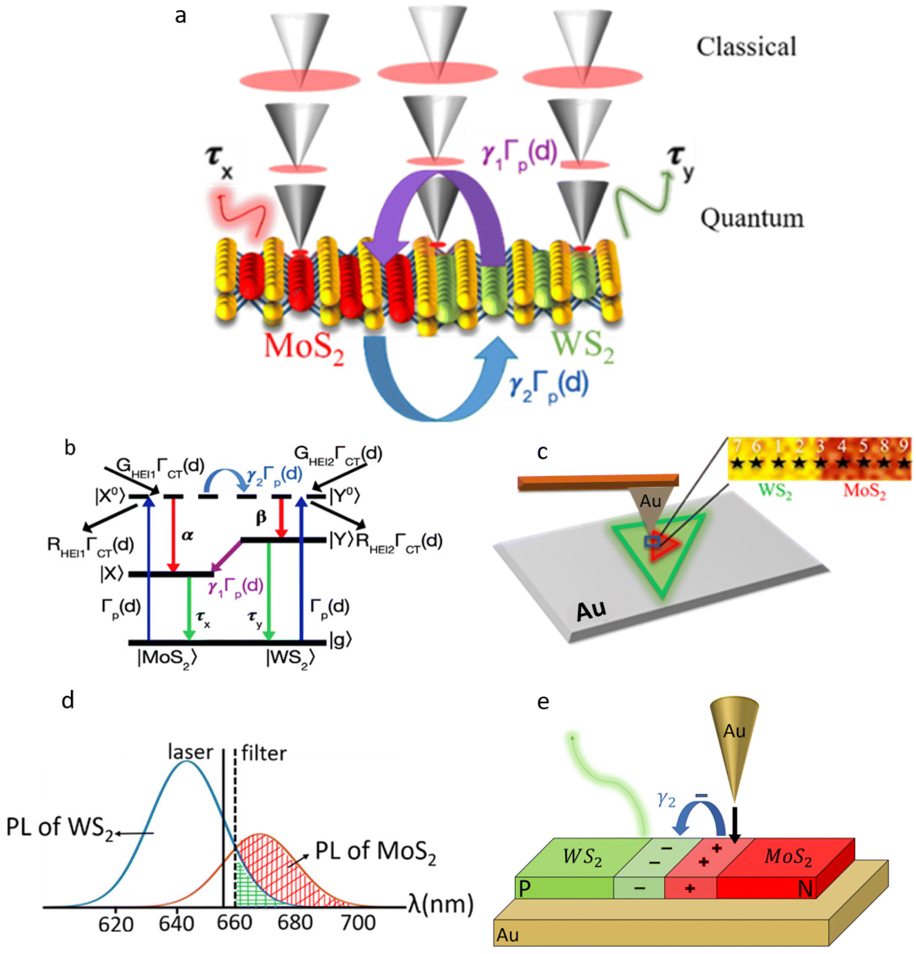 | ||
| Fig. 1 (a) Sketch of the tip–sample distance (TSD) dependence PL measurements of a lateral WS2–MoS2 heterostructure in the classical (TSD > 0.36 nm) and quantum (TSD < 0.36 nm) regimes. Electric field excitation spots (red ovals) decrease with the decrease of TSD. (b) The schematic energy level diagram of the 2D lateral heterojunction shows hot electron injection (HEI) from the plasmonic tip to the heterostructure accompanied by the nonresonant (γ1, purple arrow) and resonant (γ2, blue arrow) charge transfer. (c) Tip–sample configuration in tip-enhanced photoluminescence (TEPL) experiments. Inset shows an AFM phase image of a part of the heterostructure including the WS2–MoS2 junction and locations 1–9 of TSD measurements. (d) Sketch of the PL signals of WS2 (green shaded area) and MoS2 (red shaded area) including the laser (solid line) and the filter cutoff (dashed line). (e) Schematic diagram of the PL enhancement mechanism in a quantum plasmonic p–n junction. | ||
The sketch of the TEPL setup in Fig. 1c shows the plasmonic Au tip on top of the WS2–MoS2 heterostructure. The area used for TEPL measurements (blue box) includes parts of the pure WS2, MoS2, and the WS2–MoS2 junction. The inset shows the AFM phase image with marked locations of TSD measurements labeled 1–9, where spot 3 is on the junction. We chose representative spots 1–5 for the analysis below. Other spots located further away from the junction showed similar behavior that is characteristic of the pure WS2 and MoS2 materials. The distances between the spots 1–2, 2–3, 3–4, and 4–5 are 172 nm, 246 nm, 238 nm, and 231 nm, respectively.
We used a 660 nm excitation laser with a 665 nm cutoff spectral filter to block the laser background as shown in Fig. 1d. This resulted in the partial cutoff of the WS2 and MoS2 PL signals shown by the highlighted green and red shaded spectral areas in Fig. 1d, respectively. No filter was used for the corresponding PL spectra obtained with 532 nm excitation (see ESI Fig. S1 and S2†).
TSD dependent PL measurements at the S1–S5 locations across the WS2–MoS2 junction are shown in the classical and quantum regimes in Fig. 2 and 3, respectively. The 2D contour maps in Fig. 2a–e show PL intensity as a function of TSD and wavelength. The 2D contour plots were obtained by combining the PL signals at two TSD regimes, separated by the horizontal dashed lines in Fig. 2a–e. Our TSD analysis procedure was previously described.26 Briefly, we used the TSD = 0.36 nm as a reference point, which corresponds to the vdW contact distance between the Au atom of the tip and the S atom of the WS2–MoS2 heterostructure. We used the piezo motor positions as TSD values in the classical regime (above the horizontal dashed line). The TSD values in the quantum regime (below the dashed line) were obtained using our previously described fitting procedure in the repulsive range of the Lennard-Jones potential.26 Briefly, the tip and laser were kept stationary before the vdW contact, while the sample stage moved upwards. After the vdW contact, both the tip and sample moved upwards together, while the AFM cantilever bending and the tip–sample repulsive force increased. The corresponding TSD values were obtained by fitting the repulsive force as a function of the piezo position. We used the value of the A coefficient, A = 2.2 × 10⁻⁷, in the repulsive force, F = A/d13, and the cantilever spring constant of 2.8 N m−1.
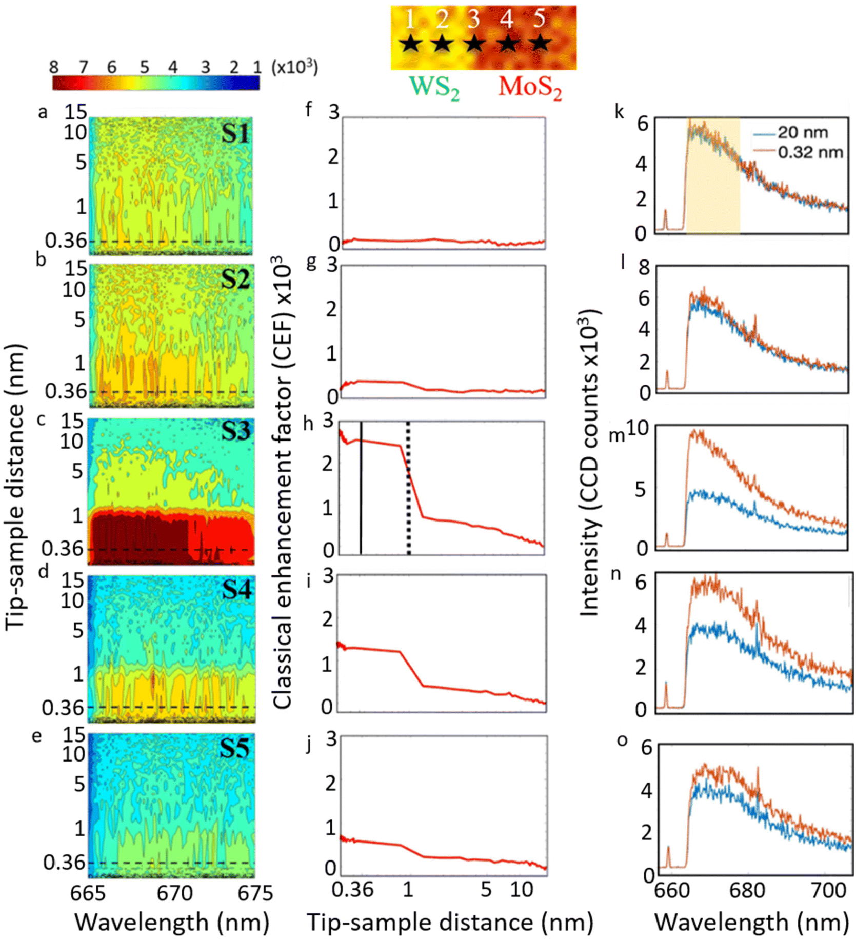 | ||
| Fig. 2 Tip–sample distance (TSD) dependent PL of WS2–MoS2 lateral heterostructure. (a–e) 2D contour plots of PL signals at various TSDs for locations S1–S5 across the junction, shown at 5 spots in the inset (marked as stars 1–5). (f–j) Classical enhancement factors and (k–o) PL spectra at the corresponding locations. PL spectral intensities are shown at 20 nm (blue) and 0.32 nm (red) TSDs. Vertical solid and dashed lines in (h) indicate the van der Waals contact and jump-to-contact TSDs, respectively. The shaded area in (k) highlights the spectral range of the integrated TSD signal. | ||
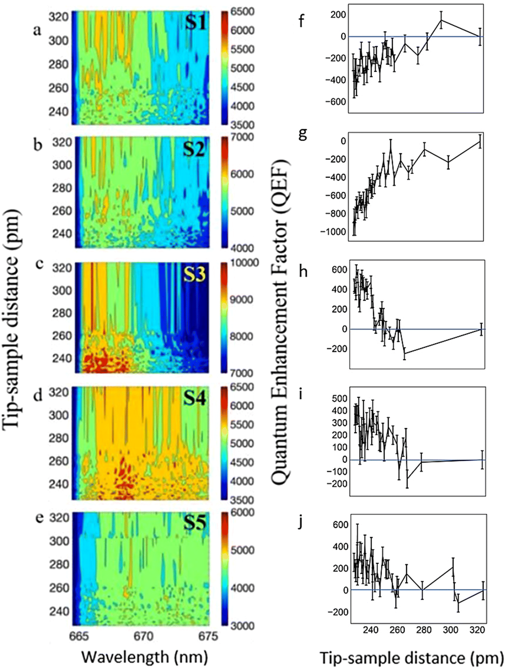 | ||
| Fig. 3 Picoscale TSD dependent PL of WS2–MoS2 lateral heterostructure in the quantum tunneling regime. (a–e) 2D contour plots and (f–j) quantum enhancement factors for the locations S1–S5 corresponding to Fig. 2. | ||
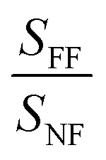
We calculated the classical and quantum enhancement factors, shown in Fig. 2 and 3, respectively, that provides quantitative analysis of the PL enhancement normalized by the contributing areas in the classical and quantum regimes. We use the conventional definition of the classical enhancement factor (CEF) as:43
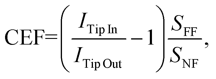 | (1) |
 of 2.5 × 10³. The resulting CEF values as a function of TSD are shown for the locations S1–S5 in Fig. 2f–j, respectively.
In the quantum plasmonic regime, we consider the tunneling effect by using the NF PL intensity at vdW contact TSD of 0.36 nm for IvdW, relative to the NF PL at TSD < 0.32 nm for IC, which approaches the conductive contact distance of 0.22 nm. The corresponding quantum EF (QEF) equation is:
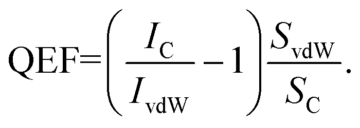 | (2) |
We assume that the PL enhancement at TSD < 0.36 nm originates from only a few atoms at the tip apex, in the limit from just one Au atom. Therefore, we use the radius of a Au atom of 0.179 nm to define the area SC. For SvdW we use the same area as above for the near field with the tip apex area of 10 nm. This gives the value of the 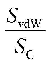 factor of 1.2 × 10⁴. The resulting QEF values as a function of TSD are shown for the locations S1–S5 in Fig. 3f–j, respectively.
By setting the SC area to one Au atom we obtained the highest estimate of QEF. This assumption is based on recent sub-nanometer resolution TERS and TEPL experiments, where a single Au or Ag atom protruding from a plasmonic tip was responsible for the signal enhancement.44–48 The QEF will decrease by taking the low estimate of the tip apex area of 10 nm. However, our experimental results better match the simulations using the single Au atom area.
We compared the CEF and QEF values at the locations S1–S5 in Table 1. The CEF value at TSD = 0.32 nm provides the estimate of the relative PL enhancement due to the near field at the tip apex interacting with the various parts of the heterostructure. The largest enhancement of 2554 was obtained at the junction in spot S3. Less than 2 orders of magnitude enhancement was obtained in spot S1 on the pure WS2. This may be attributed to the different enhancement mechanisms of the junction compared to the pure materials, as discussed below. Further suppression in spot S1 is observed in QEF by decreasing the TSD, with large negative values of QEF indicating the contribution of the traditional quantum plasmonic limit to the PL enhancement.33,34 On the other hand, at location S3 of the junction, the QEF value is large and positive, indicating the additional three orders of magnitude PL enhancement by a further decrease of TSD by a hundred pm below the vdW contact. Positive QEF is also observed at locations S4 and S5 on pure MoS2 with lower values compared to the junction. This enhancement decreases when the tip moves away from the junction.
| Spots | CEF (0.32 nm) | QEF (0.20 nm) |
|---|---|---|
| S1 | 16 | −234 |
| S2 | 219 | −966 |
| S3 | 2554 | 445 |
| S4 | 1294 | 362 |
| S5 | 587 | 259 |
Theoretical model
We used the phenomenological rate equation model to describe the interplay between hot electron injection and charge transfer across the junction that was observed in the experiments. Fig. 1b shows the schematic state diagram used to model the excited state dynamics of the WS2–MoS2 heterostructure. It shows that the initial population of the electrons excited from the ground state, |g〉, above the band gap to states |X0〉 or |Y0〉, subsequently decays to exciton states |X〉 or |Y〉. Here, |X0〉, |X〉 and |Y0〉, |Y〉 are the excited states of the MoS2 and WS2 parts of the heterostructure, respectively, which might include some degree of alloying due to the proximity to the junction. As a result, the population dynamics can be described by the following rate equations: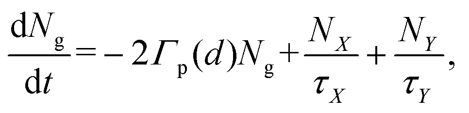 | (3) |
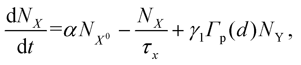 | (4) |
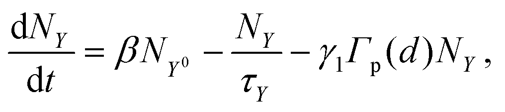 | (5) |
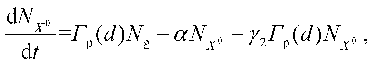 | (6) |
| Ng + NX + NY + NX0 + NY0 = 1, | (7) |
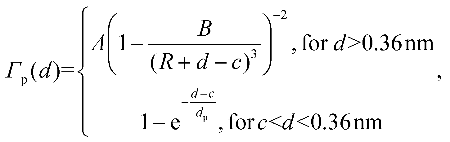 | (8) |
Fig. 4 shows the simulated PL enhancement factors for γ1 = 0 (a, b, e and f) and γ1 = 0.25 (c, d, g and h) for several values of γ2. The classical and quantum EFs were obtained using the ratios of the |X〉 and |Y〉 state populations at the TSDs corresponding to the experimental EFs defined above. The PL signals for γ1 = γ2 = 0 correspond to the pure MoS2 (a and e) and WS2 (b and f) materials. In both cases, the EF values increase in the classical and decrease in the quantum regimes (blue lines in Fig. 4a, b, e and f for γ1 = γ2 = 0). This behavior corresponds to the traditional classical/quantum plasmonics, and it is in good agreement with the experimental measurements at locations S1 (WS2) and S5 (MoS2), shown in Fig. 2f, j and 3f, j. Fig. 3j shows a small enhancement of WS2 PL due to the proximity to the junction, which disappears at locations S8 and S9 further away from the junction.
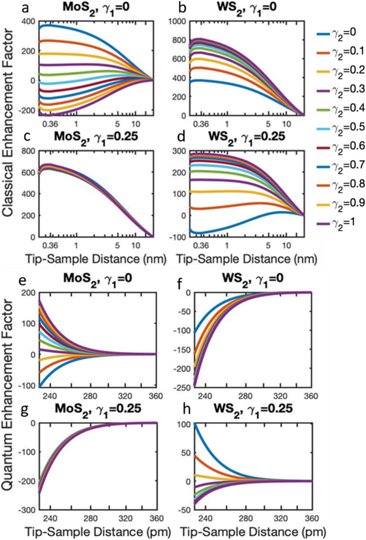 | ||
| Fig. 4 Simulated classical (a–d) and quantum (e–h) TSD dependent PL enhancement factors of WS2–MoS2 heterostructure for various values of the nonresonant (γ1) and resonant (γ2) charge transfer coefficients. The PL signals for γ1 = γ2 = 0 correspond to the pure MoS2 (a and e) and WS2 (b and f) materials (blue lines). The PL signals for γ1 = 0.25 correspond to the WS2–MoS2 junction (c, d, g and h). | ||
Discussion
Quantum plasmonic tunneling in a picocavity suppresses the PL of pure materials both under the resonant and above the band gap excitations. This has traditionally limited the plasmonic PL enhancement. For example, exciton quenching was observed by decreasing the gap size in a Au tip – Au nanotriangle plasmonic picocavity.50 It was attributed to the interplay of two effects, namely, the quantum plasmonic tunneling and the photoexcited charge transfer from MoS2 to the Au tip by exciton dissociation at the Schottky barrier.Previous work on improving the contact between 2D semiconductors and 3D metal-buried interfaces showed PL suppression by direct evaporation of Au on MoS2.51 This corresponds to the transition from vdW Au – MoS2 contact to a higher quality electronic contact, which is analogous to the decrease of TSD in our experiments. Charge transfer and local strain induce degenerate doping in MoS2. Strain may also contribute to PL modulation in our tip–sample cavity. Previous work on TEPL of nanostrained MoSe2 showed the emergence of enhanced anomalous PL from a new excitonic state localized on top of a silicon nanowire.52 However, we did not observe such a new state in our TSD experiments, and, therefore, rule out strain contribution.
Previous TEPL imaging of 2D MoSe2 revealed the cumulative effect of Purcell enhancement and oxygen induced doping leading to the enhanced biexciton emission, facilitated by the increased exciton density in the highly localized tip area.53 We did not observe any significant PL red-shift at decreasing TSD, and, therefore, ruled out the biexciton formation.
In contrast to these studies, our results showed that in TMD heterostructures it is possible to obtain an additional increase of the PL signal in the tunneling regime beyond the conventional quantum plasmonic limit. Our 660 nm excitation is near resonant with the tunneling-induced charge transfer plasmon (CTP) mode that was previously observed in a similar Au tip – Au substrate cavity.54 The role of CTP resonance in the PL enhancement is confirmed by the comparison of the resonant 660 nm excitation, which gives the 3 orders of magnitude PL enhancement (Fig. 2 and 3) to the insignificant enhancement under the nonresonant 532 nm excitation (ESI Fig. S1 and S2†). Our 2D lateral heterostructure forms a p–n junction at the interface between the two materials due to the slightly different doping in our CVD-grown materials, with p-doped WS2 and n-doped MoS2 as previously described.6 This provides an additional mechanism of PL enhancement as shown in Fig. 1e. The space charge region at the junction facilitates hot electron tunneling from the Au tip to the positively charged MoS2, while the transfer to the negatively charged WS2 region is suppressed. The charge transfer to MoS2 is increased by CTP in the quantum regime, reducing the electric field of the depletion region and increasing the charge transfer γ2 across the junction. The resulting increased carrier concentration on WS2 enhanced the PL signal. In summary, the quantum tunneling induced CTP and quantum plasmonic p–n junction mechanisms both enhanced the PL of WS2 (suppressed the PL of MoS2) in the quantum regime. Previous work showed an increase of the photoinduced charge carrier generation in a p–n junction by the electromagnetic (EM) mechanism in the classical regime.55–57 Here we attribute the tunneling in a p–n junction inside the plasmonic picocavity to a charge-transfer-based chemical mechanism (CM).58,59 We previously showed the possibility of switching from the EM to the CM mechanism in a plasmonic picocavity by decreasing the TSD.54 Here we extend this approach to a 2D heterojunction, providing new possibilities to control the optoelectronic properties of nanoscale devices.
This work may be extended to other 2D materials, such as the WSe2–MoSe2 heterostructure, by choosing the appropriate excitation source and plasmonic cavity. Our previous work on hot electron injection into the WSe2–MoSe2 heterojunction showed the opposite PL enhancement effects compared to this work. In contrast to the results on resonantly excited WS2–MoS2 heterostructure on Au substrate presented here, the previous work on WSe2–MoSe2 on SiO2/Si substrate did not have the CTP enhancement mechanism.
The simulation in Fig. 4d shows that WS2 PL is enhanced at the junction as TSD is decreased in the classical regime only when γ2 > 0.2, predicting the suppression of WS2 PL for γ2 < 0.2 in the classical regime. In addition, Fig. 4h shows the decrease of the WS2 PL at the junction in the quantum regime for γ2 > 0.3, which implies the optimal value of γ2 ∼0.25. Our model, therefore, describes the significant contribution of the CTP resonant transfer, γ2, whose TSD dependence is opposite to the nonresonant charge transfer, γ1. The interplay of these mechanisms determines the optimal values of the theoretical parameters that best describe the experimental observations.
Conclusions
In summary, we performed nanoscale PL measurements of lateral monolayer WS2–MoS2 heterostructures and observed a large increase of PL in the regime of sub-nanometer scale tip–sample distance at the location of the heterojunction. We attributed the enhancement to the interplay of the quantum plasmonic and chemical charge transfer mechanisms in the coupled 2D materials in a plasmonic picocavity. Our simulations predicted the corresponding charge transfer rates and showed good agreement with the experiments. The plasmonic tip is shown to be an efficient nano-imaging tool as well as a novel control platform.Author contributions
D.V.V. conceived the idea and designed the experiments. P.K.S. prepared the sample. D.V.V., J.L., and X.L. performed the experiments. D.V.V., S.A., Z.H.W., A.A., and A.Z. analyzed the data. Z.H.W. performed the simulations. All authors discussed and wrote the paper.Conflicts of interest
There are no conflicts to declare.References
- C. Huang, S. Wu, A. M. Sanchez, J. J. Peters, R. Beanland, J. S. Ross, P. Rivera, W. Yao, D. H. Cobden and X. Xu, Lateral Heterojunctions within Monolayer MoSe2−WSe2 Semiconductors, Nat. Mater., 2014, 13(12), 1096–1101 CrossRef CAS PubMed.
- M.-Y. Li, Y. Shi, C.-C. Cheng, L.-S. Lu, Y.-C. Lin, H.-L. Tang, M.-L. Tsai, C.-W. Chu, K.-H. Wei and J.-H. He, Epitaxial Growth of a Monolayer WSe2-MoS2 Lateral Pn Junction with an Atomically Sharp Interface, Science, 2015, 349(6247), 524–528 CrossRef CAS PubMed.
- X. Ling, Y. Lin, Q. Ma, Z. Wang, Y. Song, L. Yu, S. Huang, W. Fang, X. Zhang and A. L. Hsu, Parallel Stitching of 2D Materials, Adv. Mater., 2016, 28(12), 2322–2329 CrossRef CAS PubMed.
- M.-Y. Li, C.-H. Chen, Y. Shi and L.-J. Li, Heterostructures Based on Two-Dimensional Layered Materials and Their Potential Applications, Mater. Today, 2016, 19(6), 322–335 CrossRef CAS.
- Y. Son, M.-Y. Li, C.-C. Cheng, K.-H. Wei, P. Liu, Q. H. Wang, L.-J. Li and M. S. Strano, Observation of Switchable Photoresponse of a Monolayer WSe2−MoS2 Lateral Heterostructure via Photocurrent Spectral Atomic Force Microscopic Imaging, Nano Lett., 2016, 16(6), 3571–3577 CrossRef CAS PubMed.
- P. K. Sahoo, S. Memaran, Y. Xin, L. Balicas and H. R. Gutiérrez, One-Pot Growth of Two-Dimensional Lateral Heterostructures via Sequential Edge-Epitaxy, Nature, 2018, 553(7686), 63–67 CrossRef CAS PubMed.
- M. G. Stanford, P. D. Rack and D. Jariwala, Emerging Nanofabrication and Quantum Confinement Techniques for 2D Materials beyond Graphene, npj 2D Mater. Appl., 2018, 2(1), 1–15 CrossRef CAS.
- S. Z. Butler, S. M. Hollen, L. Cao, Y. Cui, J. A. Gupta, H. R. Gutiérrez, T. F. Heinz, S. S. Hong, J. Huang, A. F. Ismach, E. Johnston-Halperin, M. Kuno, V. V. Plashnitsa, R. D. Robinson, R. S. Ruoff, S. Salahuddin, J. Shan, L. Shi, M. G. Spencer, M. Terrones, W. Windl and J. E. Goldberger, Progress, Challenges, and Opportunities in Two-Dimensional Materials Beyond Graphene, ACS Nano, 2013, 7(4), 2898–2926 CrossRef CAS PubMed.
- Y.-M. He, G. Clark, J. R. Schaibley, Y. He, M.-C. Chen, Y.-J. Wei, X. Ding, Q. Zhang, W. Yao, X. Xu, C.-Y. Lu and J.-W. Pan, Single Quantum Emitters in Monolayer Semiconductors, Nat. Nanotechnol., 2015, 10(6), 497–502 CrossRef CAS PubMed.
- M. Turunen, M. Brotons-Gisbert, Y. Dai, Y. Wang, E. Scerri, C. Bonato, K. D. Jöns, Z. Sun and B. D. Gerardot, Quantum Photonics with Layered 2D Materials, Nat. Rev. Phys., 2022, 4(4), 219–236 CrossRef.
- W. Bao, N. J. Borys, C. Ko, J. Suh, W. Fan, A. Thron, Y. Zhang, A. Buyanin, J. Zhang and S. Cabrini, Visualizing Nanoscale Excitonic Relaxation Properties of Disordered Edges and Grain Boundaries in Monolayer Molybdenum Disulfide, Nat. Commun., 2015, 6(1), 1–7 Search PubMed.
- Y. Lee, S. Park, H. Kim, G. H. Han, Y. H. Lee and J. Kim, Characterization of the Structural Defects in CVD-Grown Monolayered MoS 2 Using near-Field Photoluminescence Imaging, Nanoscale, 2015, 7(28), 11909–11914 RSC.
- C. Lee, S. T. Kim, B. G. Jeong, S. J. Yun, Y. J. Song, Y. H. Lee, D. J. Park and M. S. Jeong, Tip-Enhanced Raman Scattering Imaging of Two-Dimensional Tungsten Disulfide with Optimized Tip Fabrication Process, Sci. Rep., 2017, 7(1), 1–7 CrossRef PubMed.
- K. K. Smithe, A. V. Krayev, C. S. Bailey, H. R. Lee, E. Yalon, Ö. B. Aslan, M. Muñoz Rojo, S. Krylyuk, P. Taheri and A. V. Davydov, Nanoscale Heterogeneities in Monolayer MoSe2 Revealed by Correlated Scanning Probe Microscopy and Tip-Enhanced Raman Spectroscopy, ACS Appl. Nano Mater., 2018, 1(2), 572–579 CrossRef CAS.
- A. Krayev, C. S. Bailey, K. Jo, S. Wang, A. Singh, T. Darlington, G.-Y. Liu, S. Gradecak, P. J. Schuck and E. Pop, Dry Transfer of van Der Waals Crystals to Noble Metal Surfaces to Enable Characterization of Buried Interfaces, ACS Appl. Mater. Interfaces, 2019, 11(41), 38218–38225 CrossRef CAS PubMed.
- K.-D. Park, O. Khatib, V. Kravtsov, G. Clark, X. Xu and M. B. Raschke, Hybrid Tip-Enhanced Nanospectroscopy and Nanoimaging of Monolayer WSe2 with Local Strain Control, Nano Lett., 2016, 16(4), 2621–2627 CrossRef CAS PubMed.
- W. Xue, P. K. Sahoo, J. Liu, H. Zong, X. Lai, S. Ambardar and D. V. Voronine, Nano-Optical Imaging of Monolayer MoSe2-WSe2 Lateral Heterostructure with Subwavelength Domains, J. Vac. Sci. Technol., A, 2018, 36(5), 05G502 CrossRef.
- Z. He, Z. Han, J. Yuan, A. M. Sinyukov, H. Eleuch, C. Niu, Z. Zhang, J. Lou, J. Hu, D. V. Voronine and M. O. Scully, Quantum Plasmonic Control of Trions in a Picocavity with Monolayer WS2, Sci. Adv., 2019, 5(10), eaau8763 CrossRef CAS PubMed.
- L. Novotny and B. Hecht, Principles of Nano-Optics, Cambridge university press, 2012 Search PubMed.
- R. Esteban, A. G. Borisov, P. Nordlander and J. Aizpurua, Bridging Quantum and Classical Plasmonics with a Quantum-Corrected Model, Nat. Commun., 2012, 3(1), 1–9 Search PubMed.
- J. Zuloaga, E. Prodan and P. Nordlander, Quantum Description of the Plasmon Resonances of a Nanoparticle Dimer, Nano Lett., 2009, 9(2), 887–891 CrossRef CAS PubMed.
- W. Zhu and K. B. Crozier, Quantum Mechanical Limit to Plasmonic Enhancement as Observed by Surface-Enhanced Raman Scattering, Nat. Commun., 2014, 5(1), 1–8 Search PubMed.
- M. S. Tame, K. R. McEnery, Ş. Özdemir, J. Lee, S. A. Maier and M. S. Kim, Quantum Plasmonics, Nat. Phys., 2013, 9(6), 329–340 Search PubMed.
- N. J. Halas, S. Lal, W.-S. Chang, S. Link and P. Nordlander, Plasmons in Strongly Coupled Metallic Nanostructures, Chem. Rev., 2011, 111(6), 3913–3961 CrossRef CAS PubMed.
- J. A. Scholl, A. García-Etxarri, A. L. Koh and J. A. Dionne, Observation of Quantum Tunneling between Two Plasmonic Nanoparticles, Nano Lett., 2013, 13(2), 564–569 CrossRef CAS PubMed.
- Y. Zhang, D. V. Voronine, S. Qiu, A. M. Sinyukov, M. Hamilton, Z. Liege, A. V. Sokolov, Z. Zhang and M. O. Scully, Improving Resolution in Quantum Subnanometre-Gap Tip-Enhanced Raman Nanoimaging, Sci. Rep., 2016, 6(1), 1–9 CrossRef CAS PubMed.
- V. Kravtsov, S. Berweger, J. M. Atkin and M. B. Raschke, Control of Plasmon Emission and Dynamics at the Transition from Classical to Quantum Coupling, Nano Lett., 2014, 14(9), 5270–5275 CrossRef CAS PubMed.
- K. J. Savage, M. M. Hawkeye, R. Esteban, A. G. Borisov, J. Aizpurua and J. J. Baumberg, Revealing the Quantum Regime in Tunnelling Plasmonics, Nature, 2012, 491(7425), 574–577 CrossRef CAS PubMed.
- W. Zhu, R. Esteban, A. G. Borisov, J. J. Baumberg, P. Nordlander, H. J. Lezec, J. Aizpurua and K. B. Crozier, Quantum Mechanical Effects in Plasmonic Structures with Subnanometre Gaps, Nat. Commun., 2016, 7(1), 1–14 CrossRef PubMed.
- V. Kulkarni and A. Manjavacas, Quantum Effects in Charge Transfer Plasmons, ACS Photonics, 2015, 2(7), 987–992 CrossRef CAS.
- D. Xu, X. Xiong, L. Wu, X.-F. Ren, C. E. Png, G.-C. Guo, Q. Gong and Y.-F. Xiao, Quantum Plasmonics: New Opportunity in Fundamental and Applied Photonics, Adv. Opt. Photonics, 2018, 10(4), 703–756 CrossRef.
- C. Ciracì, R. T. Hill, J. J. Mock, Y. Urzhumov, A. I. Fernández-Domínguez, S. A. Maier, J. B. Pendry, A. Chilkoti and D. R. Smith, Probing the Ultimate Limits of Plasmonic Enhancement, Science, 2012, 337(6098), 1072–1074 CrossRef PubMed.
- Y. Zhang, D. V. Voronine, S. Qiu, A. M. Sinyukov, M. Hamilton, Z. Liege, A. V. Sokolov, Z. Zhang and M. O. Scully, Improving Resolution in Quantum Subnanometre-Gap Tip-Enhanced Raman Nanoimaging, Sci. Rep., 2016, 6, 25788 CrossRef CAS PubMed.
- C. Tang, Z. He, W. Chen, S. Jia, J. Lou and D. V. Voronine, Quantum Plasmonic Hot-Electron Injection in Lateral WS e2/MoSe2 Heterostructures, Phys. Rev. B, 2018, 98(4), 041402 CrossRef CAS.
- A. Albagami, S. Ambardar, H. Hrim, P. K. Sahoo, Y. Emirov, H. R. Gutiérrez and D. V. Voronine, Tip-Enhanced Photoluminescence of Freestanding Lateral Heterobubbles, ACS Appl. Mater. Interfaces, 2022, 14(8), 11006–11015 CrossRef CAS PubMed.
- T. P. White and K. R. Catchpole, Plasmon-Enhanced Internal Photoemission for Photovoltaics: Theoretical Efficiency Limits, Appl. Phys. Lett., 2012, 101(7), 073905 CrossRef.
- Y. Shi, J. Wang, C. Wang, T.-T. Zhai, W.-J. Bao, J.-J. Xu, X.-H. Xia and H.-Y. Chen, Hot Electron of Au Nanorods Activates the Electrocatalysis of Hydrogen Evolution on MoS2 Nanosheets, J. Am. Chem. Soc., 2015, 137(23), 7365–7370 CrossRef CAS PubMed.
- T. Hartman, C. S. Wondergem, N. Kumar, A. van den Berg and B. M. Weckhuysen, Surface-and Tip-Enhanced Raman Spectroscopy in Catalysis, J. Phys. Chem. Lett., 2016, 7(8), 1570–1584 CrossRef CAS PubMed.
- M. L. Brongersma, N. J. Halas and P. Nordlander, Plasmon-Induced Hot Carrier Science and Technology, Nat. Nanotechnol., 2015, 10(1), 25–34 CrossRef CAS PubMed.
- C. Clavero, Plasmon-Induced Hot-Electron Generation at Nanoparticle/Metal-Oxide Interfaces for Photovoltaic and Photocatalytic Devices, Nat. Photonics, 2014, 8(2), 95–103 CrossRef CAS.
- J. S. DuChene, B. C. Sweeny, A. C. Johnston-Peck, D. Su, E. A. Stach and W. D. Wei, Prolonged Hot Electron Dynamics in Plasmonic-Metal/Semiconductor Heterostructures with Implications for Solar Photocatalysis, Angew. Chem., Int. Ed., 2014, 53(30), 7887–7891 CrossRef CAS PubMed.
- S. Ambardar, R. Kamh, Z. H. Withers, P. K. Sahoo and D. V. Voronine, Coupling Nanobubbles in 2D Lateral Heterostructures, Nanoscale, 2022, 14(22), 8050–8059 RSC.
- B. Pettinger, P. Schambach, C. J. Villagómez and N. Scott, Tip-Enhanced Raman Spectroscopy: Near-Fields Acting on a Few Molecules, Annu. Rev. Phys. Chem., 2012, 63, 379–399 CrossRef CAS PubMed.
- R. Zhang, Y. Zhang, Z. C. Dong, S. Jiang, C. Zhang, L. G. Chen, L. Zhang, Y. Liao, J. Aizpurua, Y. Luo, J. L. Yang and J. G. Hou, Chemical Mapping of a Single Molecule by Plasmon-Enhanced Raman Scattering, Nature, 2013, 498(7452), 82–86 CrossRef CAS PubMed.
- J. Lee, K. T. Crampton, N. Tallarida and V. A. Apkarian, Visualizing Vibrational Normal Modes of a Single Molecule with Atomically Confined Light, Nature, 2019, 568(7750), 78–82 CrossRef CAS PubMed.
- B. Yang, G. Chen, A. Ghafoor, Y. Zhang, Y. Zhang, Y. Zhang, Y. Luo, J. Yang, V. Sandoghdar, J. Aizpurua, Z. Dong and J. G. Hou, Sub-Nanometre Resolution in Single-Molecule Photoluminescence Imaging, Nat. Photonics, 2020, 14(11), 693–699 CrossRef CAS.
- Y. Zhang, Z.-C. Dong and J. Aizpurua, Theoretical Treatment of Single-Molecule Scanning Raman Picoscopy in Strongly Inhomogeneous near Fields, J. Raman Spectrosc., 2021, 52(2), 296–309 CrossRef CAS.
- J.-Z. Zhu, G. Chen, T. Ijaz, X.-G. Li and Z.-C. Dong, Influence of an Atomistic Protrusion at the Tip Apex on Enhancing Molecular Emission in Tunnel Junctions: A Theoretical Study, J. Chem. Phys., 2021, 154(21), 214706 CrossRef CAS PubMed.
- C. Robert, D. Lagarde, F. Cadiz, G. Wang, B. Lassagne, T. Amand, A. Balocchi, P. Renucci, S. Tongay and B. Urbaszek, Exciton Radiative Lifetime in Transition Metal Dichalcogenide Monolayers, Phys. Rev. B, 2016, 93(20), 205423 CrossRef.
- M. Ferrera, M. Rahaman, S. Sanders, Y. Pan, I. Milekhin, S. Gemming, A. Alabastri, F. Bisio, M. Canepa and D. R. T. Zahn, Controlling Excitons in the Quantum Tunneling Regime in a Hybrid Plasmonic/2D Semiconductor Interface, Appl. Phys. Rev., 2022, 9(3), 031401 CAS.
- K. Jo, P. Kumar, J. Orr, S. B. Anantharaman, J. Miao, M. J. Motala, A. Bandyopadhyay, K. Kisslinger, C. Muratore, V. B. Shenoy, E. A. Stach, N. R. Glavin and D. Jariwala, Direct Optoelectronic Imaging of 2D Semiconductor–3D Metal Buried Interfaces, ACS Nano, 2021, 15(3), 5618–5630 CrossRef CAS PubMed.
- T. Chowdhury, K. Jo, S. B. Anantharaman, T. H. Brintlinger, D. Jariwala and T. J. Kempa, Anomalous Room-Temperature Photoluminescence from Nanostrained MoSe2 Monolayers, ACS Photonics, 2021, 8(8), 2220–2226 CrossRef CAS.
- D. Moore, K. Jo, C. Nguyen, J. Lou, C. Muratore, D. Jariwala and N. R. Glavin, Uncovering Topographically Hidden Features in 2D MoSe2 with Correlated Potential and Optical Nanoprobes, npj 2D Mater. Appl., 2020, 4(1), 1–7 CrossRef.
- H. N. Hrim, S. Ambardar, A. Albagami, S. Mendenhall, M. T. Trinh and D. V. Voronine, Switching from Electromagnetic to Chemical Mechanism in Quantum Plasmonic Tip-Induced Graphene Oxide Enhanced Raman Scattering, Phys. Rev. B, 2022, 106(3), 035410 CrossRef CAS.
- P. Alonso-González, P. Albella, M. Schnell, J. Chen, F. Huth, A. García-Etxarri, F. Casanova, F. Golmar, L. Arzubiaga, L. E. Hueso, J. Aizpurua and R. Hillenbrand, Resolving the Electromagnetic Mechanism of Surface-Enhanced Light Scattering at Single Hot Spots, Nat. Commun., 2012, 3(1), 684 CrossRef PubMed.
- M. Moskovits, Surface-Enhanced Spectroscopy, Rev. Mod. Phys., 1985, 57(3), 783 CrossRef CAS.
- G. C. Schatz and R. P. Van Duyne, Image, Field Theory of Enhanced Raman Scattering by Molecules Adsorbed on Metal Surfaces: Detailed Comparison with Experimental Results, Surf. Sci., 1980, 101(1–3), 425–438 CrossRef CAS.
- H. Xu, L. Xie, H. Zhang and J. Zhang, Effect of Graphene Fermi Level on the Raman Scattering Intensity of Molecules on Graphene, ACS Nano, 2011, 5(7), 5338–5344 CrossRef CAS PubMed.
- L. Jensen, C. M. Aikens and G. C. Schatz, Electronic Structure Methods for Studying Surface-Enhanced Raman Scattering, Chem. Soc. Rev., 2008, 37(5), 1061–1073 RSC.
Footnote |
| † Electronic supplementary information (ESI) available. See DOI: https://doi.org/10.1039/d3nr00861d |
| This journal is © The Royal Society of Chemistry 2023 |