
 Open Access Article
 This Open Access Article is licensed under a Creative Commons Attribution-Non Commercial 3.0 Unported Licence
A ferromagnetic Eu–Pt surface compound grown below hexagonal boron nitride†
Alaa
Mohammed Idris Bakhit
 ab,
Khadiza
Ali
cd,
Anna A.
Makarova
e,
Igor
Píš
f,
Federica
Bondino
f,
Roberto
Sant
g,
Saroj P.
Dash
d,
Rodrigo
Castrillo-Bodero
a,
Yuri
Hasegawa
ah,
J. Enrique
Ortega
abc,
Laura
Fernandez
a and
Frederik
Schiller
*ac
ab,
Khadiza
Ali
cd,
Anna A.
Makarova
e,
Igor
Píš
f,
Federica
Bondino
f,
Roberto
Sant
g,
Saroj P.
Dash
d,
Rodrigo
Castrillo-Bodero
a,
Yuri
Hasegawa
ah,
J. Enrique
Ortega
abc,
Laura
Fernandez
a and
Frederik
Schiller
*ac
aCentro de Física de Materiales CSIC-UPV/EHU-Materials Physics Center, E-20018 San Sebastián, Spain. E-mail: frederik.schiller@csic.es
bDepartamento de Física Aplicada I, Universidad del País Vasco UPV/EHU, E-20018 San Sebastián, Spain
cDonostia International Physics Center, E-20018 Donostia-San Sebastián, Spain
dChalmers University of Technology, Göteborg, Chalmersplatsen 4, 412 96 Göteborg, Sweden
ePhysikalische Chemie, Institut für Chemie und Biochemie, Freie Universität Berlin, Arnimallee 22, 14195 Berlin, Germany
fIOM-CNR, Strada Statale 14 Km 163.5, I-34149 Trieste, Italy
gESRF, The European Synchrotron, 71 Avenue des Martyrs, CS40220, 38043 Grenoble Cedex 9, France
hDepartment of Physical Sciences, Ritsumeikan University, Kusatsu, 525-8577, Japan
First published on 21st June 2023
Abstract
One of the fundamental applications for monolayer-thick 2D materials is their use as protective layers of metal surfaces and in situ intercalated reactive materials in ambient conditions. Here we investigate the structural, electronic, and magnetic properties, as well as the chemical stability in air of a very reactive metal, Europium, after intercalation between a hexagonal boron nitride (hBN) layer and a Pt substrate. We demonstrate that Eu intercalation leads to a hBN-covered ferromagnetic EuPt2 surface alloy with divalent Eu2+ atoms at the interface. We expose the system to ambient conditions and find a partial conservation of the di-valent signal and hence the Eu–Pt interface. The use of a curved Pt substrate allows us to explore the changes in the Eu valence state and the ambient pressure protection at different substrate planes. The interfacial EuPt2 surface alloy formation remains the same, but the resistance of the protecting hBN layer to ambient conditions is reduced, likely due to a rougher surface and a more discontinuous hBN coating.
1. Introduction
Ferromagnetic two-dimensional (2D) structures are of uttermost importance in spintronics applications.1 Such 2D magnetic systems can either be 2D van der Waals (vdW) ferromagnets,2–4 or ultrathin magnetic overlayers.5 Both types of systems present quantum and topological phases,6 but achieving new exotic properties requires design and investigation of novel materials and architectures. In thin magnetic overlayers, the surface contains transition and/or rare-earth metals. The interest in such 2D ferromagnetic systems is prompted by the reduced atomic-scale size and the diversity of magnetic states that arise. Some of the 2D vdW ferromagnets can be exfoliated from bulk crystals, e.g., Fe3GeTe2![[thin space (1/6-em)]](https://www.rsc.org/images/entities/char_2009.gif) 7 or family members.8,9 However, most of them are grown by ex situ chemical vapor or atomic layer deposition.10–13 Magnetic overlayers, on the other hand side, are usually grown by physical vapor deposition under vacuum conditions, a process that does not guarantee an unique 2D layer but may lead to a multilayer system. Achieving a single 2D magnetic layer demands a detailed in situ, atomic-scale investigation, comprising structure and electronic states, as well as chemical stability in ambient conditions. 2D magnetic alloys as well as some of the vdW ferromagnets are quite reactive in air, loosing or changing their magnetic properties. Protection of such surfaces can be achieved by means of ceramic coatings, polymer protection films or deposition of non-reactive metals. Nevertheless, most of these protecting overlayers influence the magnetism of the surfaces leading to a variation of the desired properties. Recently, protection of the surfaces by graphene (Gr),14–22 hexagonal boron nitride (hBN)15,23–28 and a mixture of both materials29 is being considered. In this context, the use of a hBN protecting layer is very appealing, since it would provide close contact of the ferromagnetic material with a wide-gap semiconductor, enabling charge injection. Therefore, the question that arises is whether we can achieve a sufficiently protective hBN layer that preserves the magnetic properties of the 2D compound in ambient conditions.
7 or family members.8,9 However, most of them are grown by ex situ chemical vapor or atomic layer deposition.10–13 Magnetic overlayers, on the other hand side, are usually grown by physical vapor deposition under vacuum conditions, a process that does not guarantee an unique 2D layer but may lead to a multilayer system. Achieving a single 2D magnetic layer demands a detailed in situ, atomic-scale investigation, comprising structure and electronic states, as well as chemical stability in ambient conditions. 2D magnetic alloys as well as some of the vdW ferromagnets are quite reactive in air, loosing or changing their magnetic properties. Protection of such surfaces can be achieved by means of ceramic coatings, polymer protection films or deposition of non-reactive metals. Nevertheless, most of these protecting overlayers influence the magnetism of the surfaces leading to a variation of the desired properties. Recently, protection of the surfaces by graphene (Gr),14–22 hexagonal boron nitride (hBN)15,23–28 and a mixture of both materials29 is being considered. In this context, the use of a hBN protecting layer is very appealing, since it would provide close contact of the ferromagnetic material with a wide-gap semiconductor, enabling charge injection. Therefore, the question that arises is whether we can achieve a sufficiently protective hBN layer that preserves the magnetic properties of the 2D compound in ambient conditions.
Here, we study a hBN-protected ferromagnetic Eu–Pt surface alloy. The Eu–Pt compound is formed after Eu intercalation under the hBN film previously grown on a Pt crystal surface. Metal intercalation below Gr or hBN overlayer has been extensively studied over the last two decades.20–22,30–32 The purpose in the majority of the works was to separate the 2D overlayer from the substrate.33,34 Most often this is done by the intercalation of noble metal atoms like Au, Ag, or Cu.33 Conversely, in order to force a stronger 2D material interface interaction, one can proceed with the intercalation of alkaline35 or earth-alkaline metals.36–38 If a too-strongly interacting substrate-2D overlayer is achieved, additional intercalation of oxygen lifts again the 2D layer and re-establishes the original 2D material properties.20 However, oxygen exposure may result in the oxidation of the protecting hBN layer.39 Eu intercalation has been less investigated21,22,30,40,41 despite of its interesting magnetic properties, mainly due to the strong reactivity of this rare earth metal.
All Eu intercalation studies have been carried out on graphite or graphene epilayers, but no experiments exist using hBN.
Among the different rare earth metal compounds, europium alloys are particularly interesting due to the various valence states of the Eu atoms. It may adopt a di-valent Eu2+, a tri-valent Eu3+, or even a mixed-valent state. For trivalent Eu3+, Eu has a 4f6 configuration with S = L = 3 and J = 0. The ground state J-multiplet level (in 2S+1LJ configuration) is 7F0 presenting a non-magnetic singlet. This situation differs from divalent Eu2+ with 4f7 configuration, S = 7/2, L = 0 and J = 7/2 leading to a 8S7/2 ground state. In the latter case, Eu2+ is able to form ferromagnetic compounds, e.g., europium chalcogenides.42 The different valence states of Eu are found to depend on several factors: the surrounding material, the lattice pressure, the number and type of nearest neighbors, etc. In the particular case of Eu–Pt bulk compounds there is a smooth valence transition when changing the stoichiometry from EuPt5 (completely tri-valent) to EuPt2 (Eu atoms in a di-valent state).43–45 Additionally, valence instabilities can be induced in EuPt3 by high pressure.46 Valence changes may also happen at the surface due to a reduced coordination.47 Such transitions from trivalent to divalent configuration have also been observed for Eu–Ni or Eu–Pd compounds.48,49
Here we present a Eu–Pt surface alloy formed after intercalation of Eu at the hBN/Pt interface. First, we perform a structural analysis of the interface, followed by a detailed electronic and magnetic characterization of the Eu–Pt compound. We demonstrate that the topmost layer under the hBN coat is a 2D EuPt2 surface alloy, with di-valent Eu atoms that reveal ferromagnetic behavior at low temperature. Next, we check the efficiency of the hBN layer protection in ambient pressure, by analyzing the electronic properties prior and after air exposure. The sample is a platinum crystal curved around the (111) direction (c-Pt). This provides a smooth variation of the crystallographic orientation across the (macroscopic) surface, allowing us to extend the analysis of the EuPt2 alloy to vicinal Pt crystal planes, characterized by a high density of atomic steps. By scanning our different experimental (electron, photon) probes on top, we can rigorously study the influence of steps and terraces in the structural, magnetic, and electronic properties of the EuPt2 surface alloy, as well as the protecting quality of the hBN layer.
2. Experimental details
The growth and electronic properties were mainly investigated at the Nanophysics laboratory in San Sebastian, Spain using a combined system containing scanning tunneling microscopy (STM), low energy electron diffraction (LEED), X-ray photoemission (XPS) and angle-resolved photoemission spectroscopy (ARPES). Part of the electronic structure investigations have been carried out at BACH beamline of Elettra synchrotron (Trieste, Italy). The XPS setup in the laboratory is equipped with a Specs Al Kα μ-FOCUS 600 monochromator while the ultraviolet light source consists of a Specs UVS-300 discharge lamp with monochromator (Specs TMM 304) tuned to HeIIα light with hν = 40.8 eV. At Elettra synchrotron, p-polarized light was applied. All measurements were taken with the sample at room temperature. STM experiments were carried out in a Omicron VT-setup by holding the sample at room temperature and scanning with a W tip. The analysis of the STM images has been performed with WSXM software.50 The magnetic properties were investigated at ID 32 of the European synchrotron radiation facility (ESRF) by means of X-ray magnetic circular dichroism (XMCD). For this purpose the sample was placed normal or grazing (70°) with respect to the incoming photon beam and field. The field was ramped between +6 and −6 T with the sample hold at T = 7 K. Horizontal, left and right circularly polarized light (99% polarization) was used for photon energies around the Eu M4,5 X-ray absorption edge.As a substrate material, a cylindrical sector of a Pt (c-Pt) single crystal was used whose cylinder axis is along a [1![[1 with combining macron]](https://www.rsc.org/images/entities/char_0031_0304.gif) 0] direction. The centre of the curved surface points towards the [111] direction, while the borders are oriented ±15° with respect to the (111) center (Fig. 4). This curved Pt surface was cleaned by Ar ion sputtering (room temperature) and temperature annealing (1000 K) as well as by occasional oxygen heating (2 × 10⁻⁸ mbar O2, 950 K) followed by a flash in UHV to 1050 K. This standard procedure, as described elsewhere,51,52 leads to sharp LEED patterns where the typical step splitting was observed.
0] direction. The centre of the curved surface points towards the [111] direction, while the borders are oriented ±15° with respect to the (111) center (Fig. 4). This curved Pt surface was cleaned by Ar ion sputtering (room temperature) and temperature annealing (1000 K) as well as by occasional oxygen heating (2 × 10⁻⁸ mbar O2, 950 K) followed by a flash in UHV to 1050 K. This standard procedure, as described elsewhere,51,52 leads to sharp LEED patterns where the typical step splitting was observed.
hBN was grown by chemical vapor deposition (CVD) process from borazine precursor (B3H6N3) (KATCHEM spol. s r.o.). For this purpose the curved Pt crystal was held at 1020 K while borazine was dosed for 20 minutes at 2 × 10⁻⁷ mbar, i.e., for 240 L, in order to assure a complete hBN layer. Already a 100 L dosage would be enough for a complete layer.32 As can be observed in Fig. 1, this growth produces a sharp and well ordered moiré pattern in LEED at the Pt(111) position of the curved crystal. On the other substrate positions, corresponding to the vicinal surfaces in the mentioned ±15° range around (111), the LEED reveals less ordered structures with line like features pointing to a multi-facet structure.
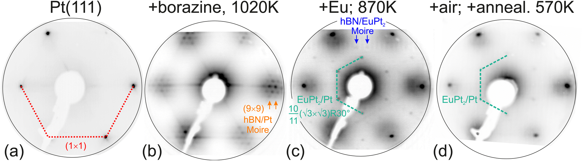 | ||
| Fig. 1 LEED images along the preparation process. (a) Pt(111), (b) after borazine exposure at 1020 K producing a (9 × 9) moiré pattern, (c) additional Eu deposition/intercalation at Tsample = 870 K leading to EuPt2 layer below hBN and a different moiré pattern, (d) after 6 hours room temperature air exposure and subsequent 570 K vacuum annealing (LEED kinetic energy 70 eV). | ||
Eu was deposited in a third step on top of this hBN/c-Pt substrate while the sample was held at an elevated temperature to allow Eu intercalation below hBN. As pointed out earlier,30 the high temperature is quite important to immediately protect the Eu from oxidation. We used substrate temperatures between 570 and 870 K. The deposition process was carried out in UHV systems with a base pressure prior to Eu deposition below 1 × 10⁻⁹ mbar not surpassing 3 × 10⁻⁹ mbar during deposition. For lower substrate temperatures incomplete intercalation takes place and part of the Eu stays on top of the hBN, see ESI† for details. The oxidation protection experiments consisted in exposing the sample to ambient pressure conditions (6 hours, room temperature, 80% humidity). The Eu thickness given throughout the manuscript corresponds to the values obtained for the calibration of the evaporator with a quartz microbalance at the measurement position. Since the sticking coefficient for both the quartz microbalance and the sample are unknown, but probably different, the indicated numbers can be compared with each other but are not suitable for absolute values.
3. Results and discussion
3.1. Formation of Eu–Pt surface alloy below hBN
:2 Pt:Eu stoichiometry of the alloy at the local atomic-scale. The pre-factor emerges from the lattice mismatch of the 2D RE-noble metal alloy layer and the substrate.
The hBN/Eu/Pt(111) system is different from the Gr/Eu/Ir(111) one,30 where the superstructure LEED spots belong to the graphene diffracted beams. In that case it was proposed that Eu forms a floating layer between the Ir(111) substrate and the graphene layer. In the here considered hBN/Eu/Pt system, however, the strongest LEED spots correspond to the EuPt2 layer at the Pt interface. As indicated in Fig. 1(c), we can still detect extra satellite spots around the 10/11·(√3 × √3)R30° structure, which arise from the coincidence lattice defined by the mismatched hBN/EuPt2 interface. Being all LEED structures properly identified, one can calculate real space lattice parameters out of the pattern. Taking into account the Pt lattice constant of aPt = 3.92 Å, we obtain the EuPt2 coincidence lattice constant of 11·aPt/√2 = 30.5 Å, from which we deduce the EuPt2 lattice parameter aEuPt2 = aPt/√2·10/11·√3 = 5.29 Å, with a nearest neighbor distance of 3.05 Å. The lattice mismatch of the EuPt2 layer with the hBN lattice on top (2.504 Å) is quite large, but explains the 4.6 × 4.6 weak superstructure spots, marked by blue arrows in Fig. 1(c). After 6 hours of air exposure and a soft annealing to 570 K to remove air adsorbates the LEED pattern still reveals the 10/11·(√3 × √3)R30° structure.
Bulk EuPt2 exists and crystalizes in a MgCu2 Laves phase structure, as shown in Fig. 2(a). A bulk lattice constant aLaves between 7.64 and 7.73 Å has been reported.43,44,61 However, in such bulk EuPt2 structure, and along the [111] direction, one cannot find any stoichiometric EuPt2 plane. Contiguous (111) planes contain either Pt and Eu solely, as shown in Fig. 2(b). The plane containing the Eu atoms is shifted by 3/8 of the densely packed Pt planes (approx. 0.8 Å). The fundamental Pt containing (111) plane is formed by a Kagomé lattice [blue layer in Fig. 2(a)], with the Eu atoms sitting above and below each Pt hexagon of the Kagomé lattice. Considering the Eu–Pt bilayer, this defines a (2 × 2) superstructure with a EuPt3 composition. The here found EuPt2 structure formed below hBN is therefore not related to bulk EuPt2 and can be understood by the simple incorporation of Eu atoms in the uppermost Pt(111) surface plane. Due to the larger size of the Eu atom, the interatomic distance at the surface increases, and a mismatch with the Pt(111) substrate underneath arises, leading to the 10/11·(√3 × √3)R30° coincidence lattice.
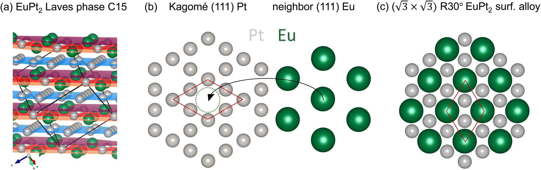 | ||
| Fig. 2 Structural Model of the EuPt2 surface. (a) Laves phase (C15) of bulk EuPt2 in the MgCu2 structure, (b) central Pt Kagomé (blue layer in (a)) and neighboring Eu(111) layer stacking inside bulk EuPt2 that would result in a PtEu3 composition with (2 × 2) superstructure after Eu incorporation, (c) (√3 × √3)R30° monolayer surface alloy structure below a 2D hBN layer. | ||
The chemical characterization of the Eu intercalation process is carried out by means of X-ray photoemission spectroscopy. Results are shown in Fig. 3. In the bulk EuPt2 compound Eu atoms are in a di-valent Eu2+ configuration, while Eu atoms in compounds with higher Pt content become mixed-valent or completely tri-valent.44 The latter situation would be the case for Eu interstitial atoms, e.g., those that diffuse into the bulk and are surrounded by Pt completely. Fig. 3 reveals the Eu 3d core level for sub- and monolayer preparations at different temperatures. Submonolayer Eu deposition and intercalation at low substrate temperature (T = 570 K) leads to a (nearly) complete divalent configuration while preparations at higher T result in the appearance of an additional Eu3+ signal. We interpret these observations as follows: at lower temperature only a partial Eu intercalation takes place, leading to the formation of EuPt2 patches below hBN (intercalated) and di-valent metallic Eu above hBN (not intercalated). For higher temperature, the Eu intercalation is complete, but together with the Eu2+ species of the EuPt2 interface below hBN, Eu3+ component arises, which is ascribed to Eu interstitials in the Pt bulk, or simply to the buildup, under the topmost EuPt2 patches, of EuPtn (n > 2) alloys, giving rise to a tri-valent or a mixed-valent situation. The Eu2O3 oxide has also Eu atoms in a tri-valent state. However, the presence of significant amounts of Eu2O3 are ruled out by the absence of an O 1s emission in XPS. The spectral region of the latter can be found in the ESI.† At higher coverage (>3 Å), preparations at both low and high temperatures already force extra Eu atoms to diffuse below the completed EuPt2 layer, leading to similar di- and tri-valent contributions in the Eu 3d XPS spectra, as shown in the top part of Fig. 3. This tri-valent contribution for low-temperature preparation prove that a considerable part of Eu intercalates already at this temperature. Increasing the temperature at high coverage enhances the bulk diffusion, and leads to even stronger Eu3+ emission compared to Eu2+.
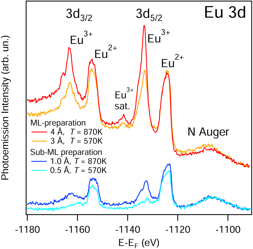 | ||
| Fig. 3 Eu 3d photoemission signal. X-ray photoemission spectra for the Eu 3d edge taken at hν = 1486.6 eV (Al Kα) for sub- and monolayer preparations at sample temperatures T = 570 K and 870 K, respectively. | ||
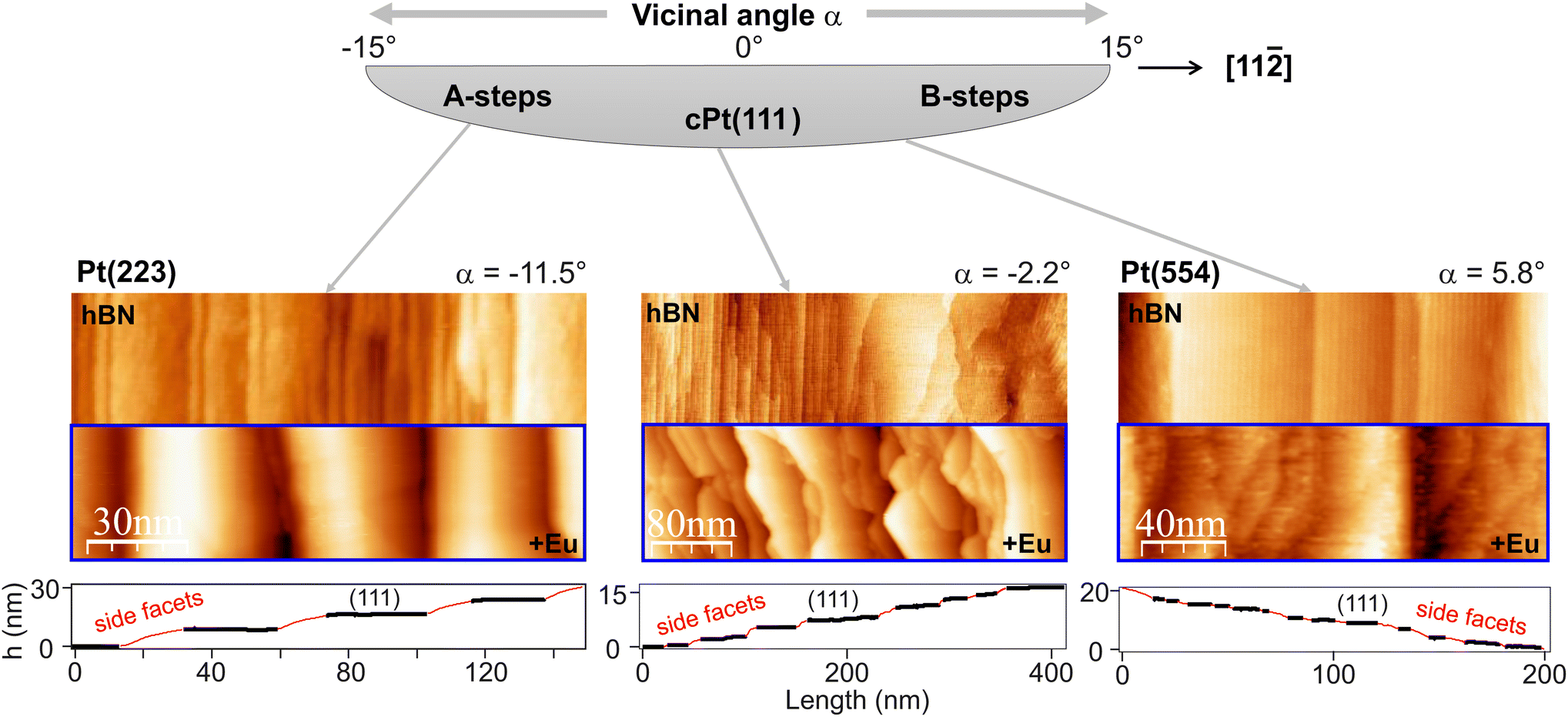 | ||
| Fig. 4 STM images of the (Eu)/hBN/c-Pt(111) system. Large scale STM images of a hBN monolayer prior and after Eu intercalation collected at three different positions on the curved c-Pt(111) substrate (scanning parameters: I = 0.13 nA; U = 0.5 V). The line scans were taken close to the top of the images corresponding to the Eu intercalated systems. (111) and side facets are indicated by different color. | ||
Eu deposition and intercalation on the vicinal surfaces changes the facet periodicity, size and inclination, as observed in the STM images. At the A-step type Pt(223) position, the rather disordered hBN/Pt(223) structure transforms into a well ordered array after Eu intercalation. On B-type steps, however, the Eu intercalation is leading to smaller facets. A statistical analysis of the STM images reveals an increasing average facet distance [(111) + side facet] of 20 facets per μm close to (111), 25 facets per μm at (223), and 65 facets per μm at (554). This means that at A-type steps the surface rugosity decreases, contrary to B-type steps. On the other hand, XPS spectra (see below) reveal a similar Eu2+/Eu3+ relation on the different crystal positions, with a slightly higher di-valent amount at (111) compared to stepped surface planes.
3.2. Magnetism of the hBN/EuPt2 system in the (111) plane
Divalent Eu (4f7, J = 7/2) has a low-temperature ferromagnetic state in bulk EuPt2 and similar compounds.68 We measured the magnetic properties of our hBN-protected EuPt2 surface alloy with X-ray circular magnetic dichroism (XMCD) at the (111) position in the curved crystal. Results are shown in Fig. 5. The X-ray absorption (XAS) spectrum in part (a) reveals a mixture of Eu2+ and Eu3+ contribution after Eu intercalation below the hBN/Pt(111) surface. This observation confirms the coexistence of the two Eu valences and it is consistent with the XPS results, namely di-valent Eu atoms at the EuPt2 surface and tri-valent Eu atoms diffused into the Pt bulk. The XMCD signal results from the difference of the absorption spectra of left and right circularly polarized light and is shown in the bottom of Fig. 5(a). At the applied field of 6 T, it shows the typical lineshape of pure di-valent Eu.69 This is expected since, as stated before, Eu3+ has a 4f6 configuration with S = L = 3 and J = 0, hence the Eu3+ signal should not contribute significantly to the anisotropy.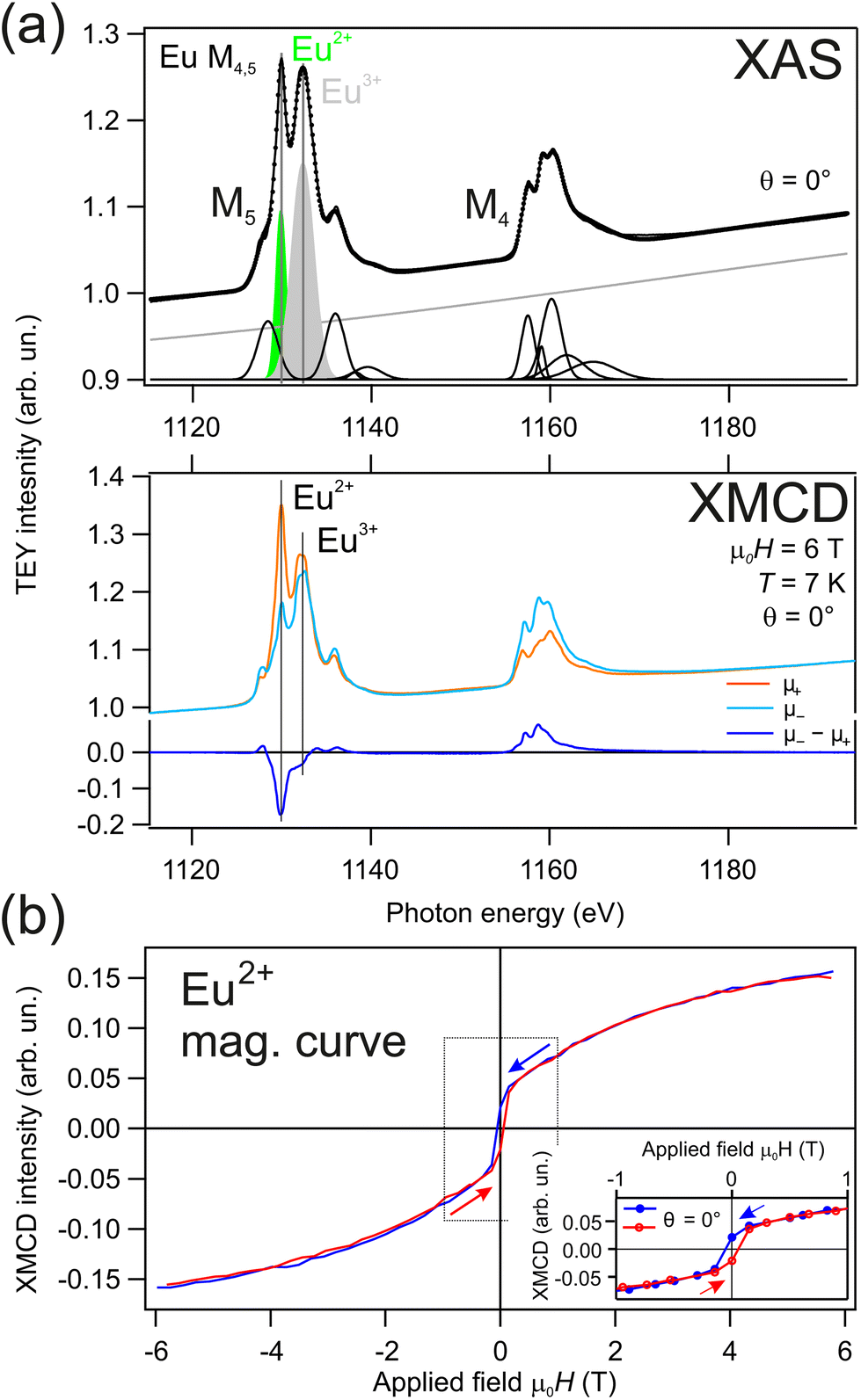 | ||
| Fig. 5 Magnetic properties of intercalated Eu below hBN/Pt(111). (a) X-ray absorption spectrum (total electron yield – TEY) of horizontally (top, XAS) and circularly polarized light with opposite sign and its resulting difference spectrum shown below (XMCD) of 3 Å Eu intercalated below hBN/Pt(111) at a substrate temperature of 770 K. The XAS spectrum was fitted with several gaussian profiles (black, grey, green) and a linear background (grey line) for each of the two main Eu2+ and Eu3+ contributions. (b) Magnetization curve taken at the maximum of the Eu M5 XMCD signal for a variable applied field from +6 T to −6 T (blue) and in the opposite direction (red), respectively. The sample was oriented perpendicular to the applied field at temperature T = 7 K. The inset presents a zoom-in to the small field region. | ||
Ferromagnetism can be probed by measuring the Eu XMCD signal while varying the applied magnetic field. The XMCD signal is proportional to the magnetization M in the system. The resulting magnetization curve is shown in Fig. 5(b). It reveals a “S” shape-like behaviour with some jump close to zero-field. Ferromagnetism is confirmed by the small hysteresis opening, which is better observed in the inset of Fig. 5(b). The corresponding XMCD spectrum after removing the applied field (remanent state) is shown in the ESI.† Another method for determining the ferromagnetic state is the Arrott plot analysis,70 which is also presented in the ESI.† For the in-plane geometry, with the sample at 70° with respect to the magnetic field and light incidence, the magnetization curve is even more “S”-shaped at small fields, pointing to an out-of-plane easy axis (see ESI† for more details).
3.3. Exposure of the hBN/Eu/Pt system to air
Fig. 6(a) displays the complete evolution of the XPS spectra during the intercalation of 4 Å-Eu in the hBN/Pt(111) interface and after exposure to air. Prior to Eu intercalation, we obtain the characteristic shape and positions in the B 1s and N 1s core levels for the weakly-coupled hBN/Pt(111) system.53 Individual contributions of the emissions can be extracted from line fittings, that are shown with further details in the ESI.† After Eu intercalation B 1s and N 1s core levels notably change their shape and energy, reflecting the fact that the hBN contact interface is now different. There are emissions from areas where the hBN layer is still contacting to Pt without Eu intercalation, giving rise to the right hand side emission, and areas for hBN on EuPt2, to which we assign the additional peaks that appear shifted to high binding energy. Such a shift is also observed for the hBN/Rh(111) interface, pointing to a similarly strongly interacting hBN/PtEu2 interface.53 With respect to the Eu core level, as mentioned above, it proves that Eu atoms are present in two configurations, di-valent Eu2+ for the 2D EuPt2 alloy and tri-valent Eu3+ for Eu atoms incorporated into the Pt bulk below the EuPt2 layer. After sample exposition to ambient conditions (6 hours, room temperature, 80% humidity) and a vacuum annealing to 770 K to remove at least part of impurities from the air exposure, the ratio of Eu2+/Eu3+ drops to one third. Note, that also the other core level intensities shrink. This relates to the appearance of adventitious C 1s (see ESI†) and O 1s emissions. The O 1s core level is detected at the higher binding energy side of the Pt 4p3/2 spectrum. A detailed view (inset) indicates a double-peak with energy positions of 530.5 eV and 532 eV, respectively. The former is in good agreement with the binding energy in the tri-valent Eu2O3 oxide.71,72 The 532 eV emission is interpreted as due to hydroxide –OH, typical of Eu samples exposed to air. On the other hand, B 1s and N 1s core levels partially recover their shape and energy prior to Eu exposure. Especially the very strong interacting component of the hBN/EuPt2 areas disappeared while the emissions of weak interacting hBN/Eu and hBN/Pt are preserved or even increased. The latter suggests that hBN areas on oxidized Eu have a similar core level emission as the hBN/Pt system, being both very low interacting interfaces. Another result from the XPS analysis is that oxidation of the hBN layer is not observed.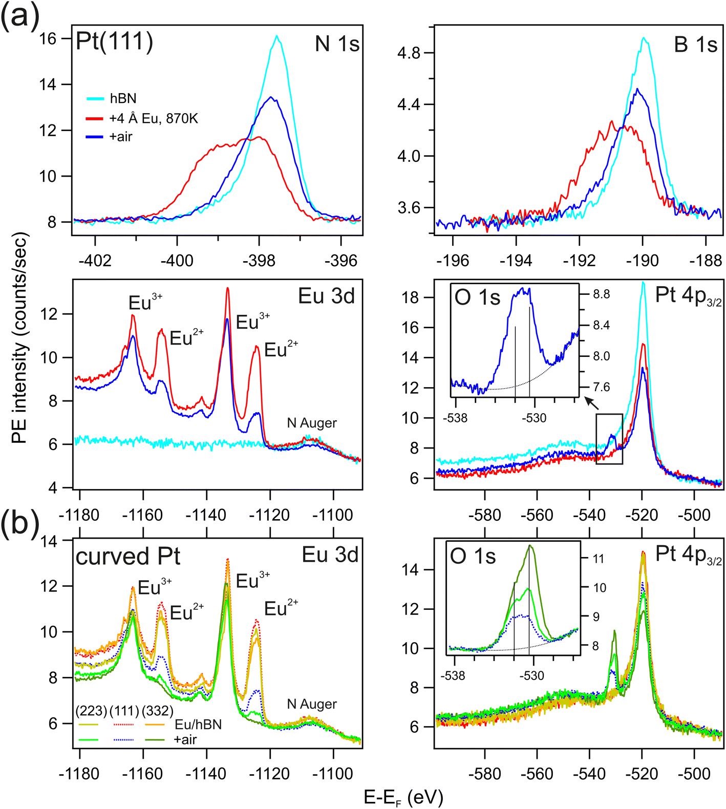 | ||
| Fig. 6 XPS analysis of Eu intercalation below hBN on the curved Pt crystal. (a) N 1s, B 1s, Eu 3d, O 1s, and Pt 4p3/2 X-ray photoemission spectra taken at hν = 1486.6 eV (Al Kα) for the Eu 4 Å preparation before and after exposing to ambient conditions at Pt(111). (b) Comparative Eu 3d, O 1s, and Pt 4p3/2 core levels at three positions of the curved Pt substrate, at Pt(332), Pt(111) and Pt(335) positions, respectively. | ||
The hBN protection for the intercalated EuPt2 alloy in vicinal Pt substrates is examined in Fig. 6(b), in direct comparison with the Pt(111) plane. Here we show the Eu 3d, Pt 4p3/2 and O 1s core levels at the Pt(332) and Pt(223) surfaces. At the Pt(332) plane, no di-valent signal remains in the Eu 3d spectrum after exposure to air. At the Pt(223) position the Eu2+/Eu3+ is strongly reduced, but the Eu2+ peak is still visible. Again, the O 1s spectrum suggests that the strong reduction of the number of di-valent Eu atoms is due to the formation of tri-valent Eu oxides and hydroxides. The overall O 1s intensity increases as the Eu2+ peak decreases at the stepped surfaces, although a more detailed peak analysis indicates that the intensity of the Eu–OH peak at 532 eV is similar in all three cases, and it is the 530.5 eV peak from Eu2O3 the one that scales reciprocally with the Eu2+/Eu3+ ratio. The complete oxidation of the B-type (332) surface correlates with the high facet density observed in the STM analysis of Fig. 4, since this allows a higher number of hBN bending or breaks at facet borders. The rather small divalent signal that remains in Pt(223) may reflect the presence of larger (111) and side facets where the intercalated EuPt2 alloy remains better protected at ambient conditions.
Finally, we analyze the impact of the air exposure on the hBN protecting layer. For this purpose angle-resolved photoemission spectroscopy (ARPES) is particularly appropriate, since it is highly sensitive to the hBN valence band, as shown in Fig. 7. The photoemission intensity map of Fig. 7(a) corresponds to the hBN/Pt(111) interface (centre of the curved sample), and has been measured using the He IIα excitation energy (hν = 40.8 eV). The strongly dispersing, intense features are the hBN π bands, with minimum at the ![[capital Gamma, Greek, macron]](https://www.rsc.org/images/entities/char_e0ba.gif) point of the Brillouin zone and maximum at
point of the Brillouin zone and maximum at ![[K with combining macron]](https://www.rsc.org/images/entities/char_004b_0304.gif) . The emissions between approx. 2 and 8 eV binding energy entirely belong to hBN, while the Pt valence band features appear closer to the Fermi level. After intercalation of a very small amount of Eu (1 Å), the main π band appears unaltered, although a replica of this band emerges below, at 2 eV higher binding energy (Fig. 7(b)). The unaltered band corresponds to hBN π-band emissions of pure Pt areas without Eu while the shifted band arises in areas where the Eu intercalates. The band shift is explained by the enhanced interaction of the hBN with the EuPt2 substrate, with a net electron transfer from Eu atoms to the hBN layer similar to other systems.40,73–75 After air exposure all bands get quite blurry, due to adsorbates. The adsorbate layer is disordered, which has the consequence that substrate and interface emissions are not well diffracted, decreasing the band intensity and increasing the background in second electron emissions. The dominating hBN π band is still visible, slightly shifted to higher binding energies. Interestingly, both the pure hBN/Pt and the Eu-intercalated bands can be recovered by annealing the sample again to 770 K, which removes adsorbates from the surface. First, this indicates that the oxygen exposure does not affect (oxidize) the hBN layer, which remains intact. Second, the photoemission intensity mapping still includes the higher binding energy replica, indicating that at least part of the strongly interacting hBN/EuPt2 patches remain, despite the oxidation of another part of the EuPt2 layer as observed in the XPS. Third, above the oxidized part, the pi-band of the hBN layer is expected to present an energy position similar to the original hBN/Pt(111) π band position since the charge transfer from the metallic Eu has disappeared and the interaction at hBN/Pt or hBN/oxide interfaces is weak in both cases. This leads to two very similar π-bands that cannot be resolved. In the supporting material we present data from the -point emission of a preparation of 4 Å Eu where this effect is better observed (see ESI†).
. The emissions between approx. 2 and 8 eV binding energy entirely belong to hBN, while the Pt valence band features appear closer to the Fermi level. After intercalation of a very small amount of Eu (1 Å), the main π band appears unaltered, although a replica of this band emerges below, at 2 eV higher binding energy (Fig. 7(b)). The unaltered band corresponds to hBN π-band emissions of pure Pt areas without Eu while the shifted band arises in areas where the Eu intercalates. The band shift is explained by the enhanced interaction of the hBN with the EuPt2 substrate, with a net electron transfer from Eu atoms to the hBN layer similar to other systems.40,73–75 After air exposure all bands get quite blurry, due to adsorbates. The adsorbate layer is disordered, which has the consequence that substrate and interface emissions are not well diffracted, decreasing the band intensity and increasing the background in second electron emissions. The dominating hBN π band is still visible, slightly shifted to higher binding energies. Interestingly, both the pure hBN/Pt and the Eu-intercalated bands can be recovered by annealing the sample again to 770 K, which removes adsorbates from the surface. First, this indicates that the oxygen exposure does not affect (oxidize) the hBN layer, which remains intact. Second, the photoemission intensity mapping still includes the higher binding energy replica, indicating that at least part of the strongly interacting hBN/EuPt2 patches remain, despite the oxidation of another part of the EuPt2 layer as observed in the XPS. Third, above the oxidized part, the pi-band of the hBN layer is expected to present an energy position similar to the original hBN/Pt(111) π band position since the charge transfer from the metallic Eu has disappeared and the interaction at hBN/Pt or hBN/oxide interfaces is weak in both cases. This leads to two very similar π-bands that cannot be resolved. In the supporting material we present data from the -point emission of a preparation of 4 Å Eu where this effect is better observed (see ESI†).
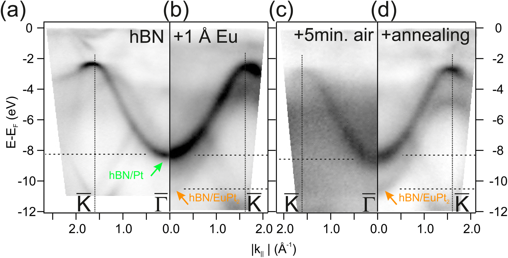 | ||
| Fig. 7 Angle resolved Photoemission analysis of the hBN layer. He IIα (hν = 40.8 eV) photoemission intensity maps along direction of the hBN band structure for (a) hBN/Pt(111), (b) after intercalation of 1 Å of Eu at T = 770 K, (c) exposure of that sample to air, and (d) after another annealing to 770 K to desorb air contamination, respectively. The most intense features correspond to the π-band of hBN at the indicated interfaces. | ||
4. Conclusions
We have investigated the structural, magnetic and electronic properties of Eu after intercalation between a Pt substrate and a hBN monolayer. We used a Pt sample curved around the (111) direction in order to additionally assess the role of substrate steps. Our LEED analysis of the (111) interface shows a ∼(√3 × √3)R30° pattern, revealing the presence of the EuPt2 surface alloy under the hBN layer. We find that Eu atoms in this EuPt2 layer are divalent, while Eu atoms that have diffused further inside the Pt bulk during the intercalation process are trivalent. Interestingly, the Eu2+/Eu3+ ratio is not affected by the presence of steps at the Pt substrate. XMCD magnetization curves on the di-valent Eu atom reveal a ferromagnetic behavior. Air exposure of the sample leads to a partial protection of the divalent Eu atoms at the (111) plane, while at vicinal surfaces the protecting role of the hBN layer is less efficient, as reflected in the larger attenuation of the divalent Eu state. Such incomplete protection of vicinal planes may be related to a larger number of defects and domain boundaries in a more discontinuous hBN layer, since this covers a much rougher hill-and-valley faceted structure. This facilitates oxygen diffusion, intercalation and the EuPt2 alloy oxidation. In contrast, the hBN layer itself remains intact upon both Eu intercalation and air exposure.Author contributions
A. M. I. B., K. A., and F. S. conceived and designed the work. A. M. I. B., K. A., A. A. M., I. P., F. B., L. F., and F. S. carried out structure and photoemission data collection while the data were analyzed and interpreted by A. M. I. B., K. A., and F. S. The magnetic measurements were performed by A. M. I. B., R. S., R. C., Y. H., L. F. and F. S. The article was drafted by A. M. I. B., J. E. O., and F. S. All authors contributed in the critical revision of the article and its final approval.Conflicts of interest
There are no conflicts to declare.Acknowledgements
We acknowledge financial support from grants PID2020-116093RB-C44 funded by the Spanish MCIN/AEI/10.13039/501100011033 and the Basque Government (Grant IT-1591-22) as well as from the German BMBF (grant 05K19KER). We acknowledge the European Synchrotron Radiation Facility for provision of beam time on ID32. ESRF access was provided through proposal MA-5454.76 Part of the research leading to the results has been supported by the project CALIPSOplus under Grant Agreement 730872 from the EU Framework Programme for Research and Innovation HORIZON 2020. Y. H. appreciates the support of Japan Society for the Promotion of Science (JSPS) Overseas Research Fellowships and I. P. and F. B. acknowledge financial support from EUROFEL project (RoadMap Esfri).References
- M. Cinchetti, V. A. Dediu and L. E. Hueso, Activating the molecular spinterface, Nat. Mater., 2017, 16, 507–515 CrossRef CAS PubMed.
- C. Gong, L. Li, Z. Li, H. Ji, A. Stern, Y. Xia, T. Cao, W. Bao, C. Wang and Y. Wang, et al., Discovery of intrinsic ferromagnetism in two-dimensional van der Waals crystals, Nature, 2017, 546(7657), 265–269 CrossRef CAS PubMed.
- B. Huang, G. Clark, E. Navarro-Moratalla, D. R. Klein, R. Cheng, K. L. Seyler, D. Zhong, E. Schmidgall, M. A. McGuire and D. H. Cobden, et al., Layer-dependent ferromagnetism in a van der Waals crystal down to the monolayer limit, Nature, 2017, 546(7657), 270–273 CrossRef CAS PubMed.
- Q. H. Wang, A. Bedoya-Pinto, M. Blei, A. H. Dismukes, A. Hamo, S. Jenkins, M. Koperski, Y. Liu, Q. C. Sun, E. J. Telford, H. H. Kim, M. Augustin, U. Vool, J. X. Yin, L. H. Li, A. Falin, C. R. Dean, F. Casanova, R. F. L. Evans, M. Chshiev, A. Mishchenko, C. Petrovic, R. He, L. Zhao, A. W. Tsen, B. D. Gerardot, M. Brotons-Gisbert, Z. Guguchia, X. Roy, S. Tongay, Z. Wang, M. Z. Hasan, J. Wrachtrup, A. Yacoby, A. Fert, S. Parkin, K. S. Novoselov, P. Dai, L. Balicas and E. J. G. Santos, The magnetic genome of two-dimensional van der Waals materials, ACS Nano, 2022, 16(5), 6960–7079 CrossRef CAS PubMed.
- P. Gambardella and S. Blügel, Magnetic Surfaces, Thin Films and Nanostructures, Springer International Publishing, Cham, 2020, pp. 625–698. ISBN 978-3-030-46906-1 Search PubMed.
- K. S. Burch, D. Mandrus and J. G. Park, Magnetism in two-dimensional van der Waals materials, Nature, 2018, 563, 47–52 CrossRef CAS PubMed.
- Z. Fei, B. Huang, P. Malinowski, W. Wang, T. Song, J. Sanchez, W. Yao, D. Xiao, X. Zhu, A. F. May, W. Wu, D. H. Cobden, J. H. Chu and X. Xu, Two-dimensional itinerant ferromagnetism in atomically thin Fe3GeTe2, Nat. Mater., 2018, 17, 778–782 CrossRef CAS PubMed.
- H. Zhang, R. Chen, K. Zhai, X. Chen, L. Caretta, X. Huang, R. V. Chopdekar, J. Cao, J. Sun, J. Yao, R. Birgeneau and R. Ramesh, Itinerant ferromagnetism in van der Waals Fe5−xGeTe2 crystals above room temperature, Phys. Rev. B, 2020, 102, 064417 CrossRef CAS.
- X. Chen, Y. T. Shao, R. Chen, S. Susarla, T. Hogan, Y. He, H. Zhang, S. Wang, J. Yao, P. Ercius, D. A. Muller, R. Ramesh and R. J. Birgeneau, Pervasive beyond room-temperature ferromagnetism in a doped van der Waals magnet, Phys. Rev. Lett., 2022, 128, 217203 CrossRef CAS PubMed.
- A. K. Geim and I. V. Grigorieva, van der Waals heterostructures, Nature, 2013, 499, 1476–4687 CrossRef PubMed.
- M. Gibertini, M. Koperski, A. F. Morpurgo and K. S. Novoselov, Magnetic 2D materials and heterostructures, Nat. Nanotechnol., 2019, 14, 408–419 CrossRef CAS PubMed.
- C. Gong and X. Zhang, Two-dimensional magnetic crystals and emergent heterostructure devices, Science, 2019, 363(6428), eaav4450 CrossRef CAS PubMed.
- K. Lasek, P. M. Coelho, K. Zberecki, Y. Xin, S. K. Kolekar, J. Li and M. Batzill, Molecular beam epitaxy of transition metal (ti-, v-, and cr-) tellurides: From monolayer ditellurides to multilayer self-intercalation compounds, ACS Nano, 2020, 14(7), 8473–8484 CrossRef CAS PubMed.
- J. Coraux, A. T. N'Diaye, N. Rougemaille, C. Vo-Van, A. Kimouche, H. X. Yang, M. Chshiev, N. Bendiab, O. Fruchart and A. K. Schmid, Air-Protected Epitaxial Graphene/Ferromagnet Hybrids Prepared by Chemical Vapor Deposition and Intercalation, J. Phys. Chem. Lett., 2012, 3(15), 2059–2063 CrossRef CAS.
- Z. Liu, Y. Gong, W. Zhou, L. Ma, J. Yu, J. C. Idrobo, J. Jung, A. H. MacDonald, R. Vajtai, J. Lou and P. M. Ajayan, Epitaxial single-crystal hexagonal boron nitride multilayers on Ni (111), Nat. Commun., 2013, 4, 2541 CrossRef PubMed.
- M. B. Martin, B. Dlubak, R. S. Weatherup, M. Piquemal-Banci, H. Yang, R. Blume, R. Schloegl, S. Collin, F. Petroff, S. Hofmann, J. Robertson, A. Anane, A. Fert and P. Seneor, Protecting nickel with graphene spin-filtering membranes: A single layer is enough, Appl. Phys. Lett., 2015, 107(1), 012408 CrossRef.
- R. S. Weatherup, L. D'Arsié, A. Cabrero-Vilatela, S. Caneva, R. Blume, J. Robertson, R. Schloegl and S. Hofmann, Long-term passivation of strongly interacting metals with single-layer graphene, J. Am. Chem. Soc., 2015, 137(45), 14358–14366 CrossRef CAS PubMed.
- M. Cattelan, G. W. Peng, E. Cavaliere, L. Artiglia, A. Barinov, L. T. Roling, M. Favaro, I. Piš, S. Nappini, E. Magnano, F. Bondino, L. Gavioli, S. Agnoli, M. Mavrikakis and G. Granozzi, The nature of the Fe-graphene interface at the nanometer level, Nanoscale, 2015, 7, 2450–2460 RSC.
- H. Naganuma, V. Zatko, M. Galbiati, F. Godel, A. Sander, C. Carrétéro, O. Bezencenet, N. Reyren, M. B. Martin, B. Dlubak and P. Seneor, A perpendicular graphene/ferromagnet electrode for spintronics, Appl. Phys. Lett., 2020, 116(17), 173101 CrossRef.
- P. Sutter, J. T. Sadowski and E. A. Sutter, Chemistry under cover: tuning metal- graphene interaction by reactive intercalation, J. Am. Chem. Soc., 2010, 132(23), 8175–8179 CrossRef CAS PubMed.
- I. S. Sokolov, D. V. Averyanov, O. E. Parfenov, I. A. Karateev, A. N. Taldenkov, A. M. Tokmachev and V. G. Storchak, 2D ferromagnetism in europium/graphene bilayers, Mater. Horiz., 2020, 7(5), 1372–1378 RSC.
- N. A. Anderson, M. Hupalo, D. Keavney, M. C. Tringides and D. Vaknin, Intercalated europium metal in epitaxial graphene on SiC, Phys. Rev. Mater., 2017, 1(5), 054005 CrossRef.
- S. Caneva, M. B. Martin, L. D'Arsié, A. I. Aria, H. Sezen, M. Amati, L. Gregoratti, H. Sugime, S. Esconjauregui, J. Robertson, S. Hofmann and R. S. Weatherup, From Growth Surface to Device Interface: Preserving Metallic Fe under Monolayer Hexagonal Boron Nitride, ACS Appl. Mater. Interfaces, 2017, 9(35), 29973–29981 CrossRef CAS PubMed.
- L. Jiang, N. Xiao, B. Wang, E. Grustan-Gutierrez, X. Jing, P. Babor, M. Kolíbal, G. Lu, T. Wu, H. Wang, F. Hui, Y. Shi, B. Song, X. Xie and M. Lanza, High-resolution characterization of hexagonal boron nitride coatings exposed to aqueous and air oxidative environments, Nano Res., 2017, 10(35), 2046–2055 CrossRef CAS.
- X. Tang, H. Wang, C. Liu, X. Zhu, W. Gao and H. Yin, Direct growth of hexagonal boron nitride nanofilms on stainless steel for corrosion protection, ACS Appl. Nano Mater., 2021, 4(11), 12024–12033 CrossRef CAS.
- J. Holler, L. Bauriedl, T. Korn, A. Seitz, F. Özyigit, M. Eichinger, C. Schüller, K. Watanabe, T. Taniguchi, C. Strunk and N. Paradiso, Air tightness of hBN encapsulation and its impact on Raman spectroscopy of van der Waals materials, 2D Mater., 2019, 7, 015012 CrossRef.
- S. Zihlmann, P. Makk, C. A. F. Vaz and C. Schönenberger, Role of hexagonal boron nitride in protecting ferromagnetic nanostructures from oxidation, 2D Mater., 2016, 3(1), 011008 CrossRef.
- K. Y. Ma, L. Zhang, S. Jin, Y. Wang, S. I. Yoon, H. Hwang, J. Oh, D. S. Jeong, M. Wang, S. Chatterjee, G. Kim, A. R. Jang, J. Yang, S. Ryu, H. Y. Jeong, R. S. Ruoff, M. Chhowalla, F. Ding and H. S. Shin, Epitaxial single-crystal hexagonal boron nitride multilayers on Ni (111), Nature, 2022, 606, 88–93 CrossRef CAS PubMed.
- I. Piš, S. Nappini, F. Bondino, T. O. Menteş, A. Sala, A. Locatelli and E. Magnano, Fe intercalation under graphene and hexagonal boron nitride in-plane heterostructure on Pt(111), Carbon, 2018, 134, 274–282 CrossRef.
- S. Schumacher, F. Huttmann, M. Petrović, C. Witt, D. F. Förster, C. Vo-Van, J. Coraux, A. J. Martínez-Galera, V. Sessi, I. Vergara, R. Rückamp, M. Grüninger, N. Schleheck, F. Meyer zu Heringdorf, P. Ohresser, M. Kralj, T. O. Wehling and T. Michely, Europium underneath graphene on Ir(111): Intercalation mechanism, magnetism, and band structure, Phys. Rev. B: Condens. Matter Mater. Phys., 2014, 90, 235437 CrossRef.
- M. Scardamaglia, V. Boix, G. D'Acunto, C. Struzzi, N. Reckinger, X. Chen, A. Shivayogimath, T. Booth and J. Knudsen, Comparative study of copper oxidation protection with graphene and hexagonal boron nitride, Carbon, 2021, 171, 610–617 CrossRef CAS.
- W. Auwärter, Hexagonal boron nitride monolayers on metal supports: Versatile templates for atoms, molecules and nanostructures, Surf. Sci. Rep., 2019, 74(1), 1–95 CrossRef.
- L. Daukiya, M. Nair, M. Cranney, F. Vonau, S. Hajjar-Garreau, D. Aubel and L. Simon, Functionalization of 2D materials by intercalation, Prog. Surf. Sci., 2019, 94(1), 1–20 CrossRef CAS.
- Y. Liu, X. Liu, C. Z. Wang, Y. Han, J. W. Evans, A. Lii-Rosales, M. C. Tringides and P. A. Thiel, Mechanism of Metal Intercalation under Graphene through Small Vacancy Defects, J. Phys. Chem. C, 2021, 125(12), 6954–6962 CrossRef CAS.
- I. Demiroglu, F. M. Peeters, O. Gülseren, D. Çakır and C. Sevik, Alkali Metal Intercalation in MXene/Graphene Heterostructures: A New Platform for Ion Battery Applications, J. Phys. Chem. Lett., 2019, 10(4), 727–734 CrossRef CAS PubMed.
- A. Grubišić-Ćabo, J. C. Kotsakidis, Y. Yin, A. Tadich, M. Haldon, S. Solari, I. Di Bernardo, K. M. Daniels, J. Riley, E. Huwald, M. T. Edmonds, R. Myers-Ward, N. V. Medhekar, D. K. Gaskill and M. S. Fuhrer, Magnesium-intercalated graphene on SiC: Highly n-doped air-stable bilayer graphene at extreme displacement fields, Appl. Surf. Sci., 2021, 541, 148612 CrossRef.
- J. C. Kotsakidis, M. Currie, A. Grubišić-Ćabo, A. Tadich, R. L. Myers-Ward, M. DeJarld, K. M. Daniels, C. Liu, M. T. Edmonds, A. L. Vázquez de Parga, M. S. Fuhrer and D. K. Gaskill, Increasing the Rate of Magnesium Intercalation Underneath Epitaxial Graphene on 6H-SiC(0001), Adv. Mater. Interfaces, 2021, 8(23), 2101598 CrossRef CAS.
- J. C. Kotsakidis, A. Grubišić-Ćabo, Y. Yin, A. Tadich, R. L. Myers-Ward, M. DeJarld, S. P. Pavunny, M. Currie, K. M. Daniels, C. Liu, M. T. Edmonds, N. V. Medhekar, D. K. Gaskill, A. L. Vázquez de Parga and M. S. Fuhrer, Freestanding n-Doped Graphene via Intercalation of Calcium and Magnesium into the Buffer Layer-SiC(0001) Interface, Chem. Mater., 2020, 32(15), 6464–6482 CrossRef CAS.
- A. A. Makarova, L. Fernandez, D. Y. Usachov, A. Fedorov, K. A. Bokai, D. A. Smirnov, C. Laubschat, D. V. Vyalikh, F. Schiller and J. E. Ortega, Oxygen Intercalation and Oxidation of Atomically Thin h-BN Grown on a Curved Ni Crystal, J. Phys. Chem. C, 2019, 123(1), 593–602 CrossRef CAS.
- U. A. Schröder, M. Petrović, T. Gerber, A. J. Martínez-Galera, E. Grånäs, M. A. Arman, C. Herbig, J. Schnadt, M. Kralj and J. Knudsen, et al., Core level shifts of intercalated graphene, 2D Mater., 2016, 4(1), 015013 CrossRef.
- I. S. Sokolov, D. V. Averyanov, O. E. Parfenov, A. N. Taldenkov, I. A. Karateev, A. M. Tokmachev and V. G. Storchak, Two-dimensional ferromagnetism in Eu-intercalated few-layer graphene, J. Alloys Compd., 2021, 884, 161078 CrossRef CAS.
- T. R. McGuire and M. W. Shafer, Ferromagnetic europium compounds, J. Appl. Phys., 1964, 35(3), 984–988 CrossRef CAS.
- H. Wickman, J. Wernick, R. Sherwood and C. Wagner, Mössbauer and magnetic properties of several europium intermetallic compounds, J. Phys. Chem. Solids, 1968, 29(1), 181–182 CrossRef CAS.
- H. de Graaf, R. Thiel and K. Buschow, On the valence of Eu in Eu-Pt compounds, Physica B+C, 1980, 100(1), 81–87 CrossRef CAS.
- M. Sauer, S. Raetz, V. Ohm, M. Merkens, C. Sauer, D. Schmitz, H. Schilder and H. Lueken, Structural, Mössbauer spectroscopic and magnetochemical investigations into EuPt5, TmPt5 and TmPt3 synthesized from platinum and gaseous lanthanide, J. Alloys Compd., 1997, 246(1), 147–154 CrossRef CAS.
- M. M. Ebd-Elmeguid and H. Micklitz, Effect of valence instability on the magnetic hyperfine interaction in EuPt3 at very high pressure, J. Phys. C: Solid State Phys., 1981, 14(26), L797 CrossRef.
- B. Johansson, Valence state at the surface of rare-earth metals, Phys. Rev. B: Condens. Matter Mater. Phys., 1979, 19, 6615 CrossRef CAS.
- S. Wieling, S. L. Molodtsov, C. Laubschat and G. Behr, Electronic and crystalline structure of epitaxial EuNix films grown on Ni(111), Phys. Rev. B: Condens. Matter Mater. Phys., 2002, 65, 075415 CrossRef.
- S. Wieling, S. L. Molodtsov, T. Gantz, J. J. Hinarejos, C. Laubschat and M. Richter, Surface compounds of divalent rare-earth metals with palladium, Phys. Rev. B: Condens. Matter Mater. Phys., 1998, 58, 13219–13223 CrossRef CAS.
- I. Horcas, R. Fernández, J. M. Gómez-Rodríguez, J. Colchero, J. Gómez-Herrero and A. M. Baro, WSXM: A software for scanning probe microscopy and a tool for nanotechnology, Rev. Sci. Instrum., 2007, 78(1), 013705 CrossRef CAS PubMed.
- A. L. Walter, F. Schiller, M. Corso, L. R. Merte, F. Bertram, J. Lobo-Checa, M. Shipilin, J. Gustafson, E. Lundgren, A. X. Brión-Ríos, P. Cabrera-Sanfelix, D. Sánchez-Portal and J. E. Ortega, X-ray photoemission analysis of clean and carbon monoxide-chemisorbed platinum(111) stepped surfaces using a curved crystal, Nat. Commun., 2015, 6, 8903 CrossRef CAS PubMed.
- F. Garcia-Martinez, C. García-Fernández, J. P. Simonovis, A. Hunt, A. Walter, I. Waluyo, F. Bertram, L. R. Merte, M. Shipilin, S. Pfaff, S. Blomberg, J. Zetterberg, J. Gustafson, E. Lundgren, D. Sánchez-Portal, F. Schiller and J. E. Ortega, Catalytic Oxidation of CO on a Curved Pt(111) Surface: Simultaneous Ignition at All Facets through a Transient CO-O Complex, Angew. Chem., Int. Ed., 2020, 59(45), 20037–20043 CrossRef CAS PubMed.
- A. B. Preobrajenski, A. S. Vinogradov, M. L. Ng, E. Ćavar, R. Westerström, A. Mikkelsen, E. Lundgren and N. Mårtensson, Influence of chemical interaction at the lattice-mismatched h-BN/Rh(111) and h-BN/Pt(111) interfaces on the overlayer morphology, Phys. Rev. B: Condens. Matter Mater. Phys., 2007, 75, 245412 CrossRef.
- M. Corso, M. J. Verstraete, F. Schiller, M. Ormaza, L. Fernández, T. Greber, M. Torrent, A. Rubio and J. E. Ortega, Rare-Earth Surface Alloying: A New Phase for GdAu2, Phys. Rev. Lett., 2010, 105, 016101 CrossRef CAS PubMed.
- M. Corso, L. Fernández, F. Schiller and J. E. Ortega, Au(111)-Based Nanotemplates by Gd Alloying, ACS Nano, 2010, 4(3), 1603–1611 CrossRef CAS PubMed.
- M. Ormaza, L. Fernández, S. Lafuente, M. Corso, F. Schiller, B. Xu, M. Diakhate, M. J. Verstraete and J. E. Ortega, LaAu2 and CeAu2 surface intermetallic compounds grown by high-temperature deposition on Au(111), Phys. Rev. B: Condens. Matter Mater. Phys., 2013, 88, 125405 CrossRef.
- L. Fernández, M. Blanco-Rey, R. Castrillo-Bodero, M. Ilyn, K. Ali, E. Turco, M. Corso, M. Ormaza, P. Gargiani and M. A. Valbuena, et al., Influence of 4f filling on electronic and magnetic properties of rare earth-Au surface compounds, Nanoscale, 2020, 12(43), 22258–22267 RSC.
- C. Xu, K. Bao, Y. Que, Y. Zhuang, X. Shao, K. Wang, J. Zhu and X. Xiao, A two-dimensional ErCu2 intermetallic compound on Cu(111) with moiré-pattern-modulated electronic structures, Phys. Chem. Chem. Phys., 2020, 22, 1693–1700 RSC.
- Y. Que, Y. Zhuang, Z. Liu, C. Xu, B. Liu, K. Wang, S. Du and X. Xiao, Two-Dimensional Rare Earth-Gold Intermetallic Compounds on Au(111) by Surface Alloying, J. Phys. Chem. Lett., 2020, 11(0), 4107–4112 CrossRef CAS PubMed.
- M. Ormaza, L. Fernández, M. Ilyn, A. Magaña, B. Xu, M. J. Verstraete, M. Gastaldo, M. A. Valbuena, P. Gargiani, A. Mugarza, A. Ayuela, L. Vitali, M. Blanco-Rey, F. Schiller and J. E. Ortega, High Temperature Ferromagnetism in a GdAg2 Monolayer, Nano Lett., 2016, 16(7), 4230–4235 CrossRef CAS PubMed.
- B. Erdmann and C. Keller, Actinide(lanthanide)-noble metal alloy phases, preparation and properties, J. Solid State Chem., 1973, 7(1), 40–48 CrossRef CAS.
- L. Fernandez, A. A. Makarova, C. Laubschat, D. V. Vyalikh, D. Y. Usachov, J. E. Ortega and F. Schiller, Boron nitride monolayer growth on vicinal Ni(111) surfaces systematically studied with a curved crystal, 2D Mater., 2019, 6(2), 025013 CrossRef CAS.
- K. Ali, L. Fernández, M. A. Kherelden, A. A. Makarova, I. Piš, F. Bondino, J. Lawrence, D. G. de Oteyza, D. Y. Usachov, D. V. Vyalikh, F. J. García de Abajo, Z. M. A. El-Fattah, J. E. Ortega and F. Schiller, Atomically-Precise Texturing of Hexagonal Boron Nitride Nanostripes, Adv. Sci., 2021, 8(17), 2101455 CrossRef CAS PubMed.
- L. Wang, X. Xu, L. Zhang, R. Qiao, M. Wu, Z. Wang, S. Zhang, J. Liang, Z. Zhang, Z. Zhang, W. Chen, X. Xie, J. Zong, Y. Shan, Y. Guo, M. Willinger, H. Wu, Q. Li, W. Wang, P. Gao, S. Wu, Y. Zhang, Y. Jiang, D. Yu, E. Wang, X. Bai, Z. J. Wang, F. Ding and K. Liu, Epitaxial growth of a 100-square-centimetre single-crystal hexagonal boron nitride monolayer on copper, Nature, 2019, 570, 91 CrossRef CAS PubMed.
- T. A. Chen, C. P. Chuu, C. C. Tseng, C. K. Wen, H. S. P. Wong, S. Pan, R. Li, T. A. Chao, W. C. Chueh, Y. Zhang, Q. Fu, B. I. Yakobson, W. H. Chang and L. J. Li, Wafer-scale single-crystal hexagonal boron nitride monolayers on Cu (111), Nature, 2020, 579, 219 CrossRef CAS PubMed.
- K. V. Bets, N. Gupta and B. I. Yakobson, How the Complementarity at Vicinal Steps Enables Growth of 2D Monocrystals, Nano Lett., 2019, 19(3), 2027–2031 CrossRef CAS PubMed.
- J. Lu, P. S. E. Yeo, Y. Zheng, H. Xu, C. K. Gan, M. B. Sullivan, A. Castro Neto and K. P. Loh, Step Flow Versus Mosaic Film Growth in Hexagonal Boron Nitride, J. Am. Chem. Soc., 2013, 135, 2368–2373 CrossRef CAS PubMed.
- A. Nakamura, H. Akamine, Y. Ashitomi, F. Honda, D. Aoki, T. Takeuchi, K. Matsubayashi, Y. Uwatoko, Y. Tatetsu, T. Maehira, M. Hedo, T. Nakama and Y. Önuki, Magnetic and Fermi Surface Properties of Ferromagnets EuPd2 and EuPt2, J. Phys. Soc. Jpn., 2016, 85(8), 084705 CrossRef.
- M. Blanco-Rey, R. Castrillo-Bodero, K. Ali, P. Gargiani, F. Bertran, P. M. Sheverdyaeva, J. E. Ortega, L. Fernandez and F. Schiller, Effect of the valence state on the band magnetocrystalline anisotropy in two-dimensional rare-earth/noble-metal compounds, Phys. Rev. Res., 2022, 4, 013237 CrossRef CAS.
- A. Arrott, Criterion for ferromagnetism from observations of magnetic isotherms, Phys. Rev., 1957, 108, 1394–1396 CrossRef CAS.
- F. Mercier, C. Alliot, L. Bion, N. Thromat and P. Toulhoat, XPS study of Eu(III) coordination compounds: Core levels binding energies in solid mixed-oxo-compounds EumXxOy, J. Electron Spectrosc. Relat. Phenom., 2006, 150(1), 21–26 CrossRef CAS.
- J. P. Baltrus and M. J. Keller, Rare earth oxides Eu2O3 and Nd2O3 analyzed by XPS, Surf. Sci. Spectra, 2019, 26(1), 014001 CrossRef CAS.
- R. Larciprete, S. Ulstrup, P. Lacovig, M. Dalmiglio, M. Bianchi, F. Mazzola, L. Hornekær, F. Orlando, A. Baraldi, P. Hofmann and S. Lizzit, Oxygen switching of the epitaxial graphene-metal interaction, ACS Nano, 2012, 6(11), 9551–9558 CrossRef CAS PubMed.
- W. Jolie, F. Craes, M. Petrović, N. Atodiresei, V. Caciuc, S. Blügel, M. Kralj, T. Michely and C. Busse, Confinement of dirac electrons in graphene quantum dots, Phys. Rev. B: Condens. Matter Mater. Phys., 2014, 89, 155435 CrossRef.
- P. Pervan, P. Lazić, M. Petrović, I. Šrut Rakić, I. Pletikosić, M. Kralj, M. Milun and T. Valla, Li adsorption versus graphene intercalation on Ir(111): From quenching to restoration of the Ir surface state, Phys. Rev. B: Condens. Matter Mater. Phys., 2015, 92, 245415 CrossRef.
- A. Mohammed Idris Bakhit, F. Schiller, L. Fernandez Gomez-Recuero, R. Castrillo Bodero and Y. Hasegawa, Magnetic properties in the single molecular magnet TbPc2 insulating ferromagnet EuO2 system, European Synchrotron Radiation Facility, Data set, 2025 DOI:10.15151/ESRF-ES-886076657.
Footnote |
| † Electronic supplementary information (ESI) available: Supplementary material contains information on electron spectroscopy analysis for Eu intercalation at insufficient substrate temperatures as well as additional XPS spectra for the Eu intercalation and air exposure process. Furthermore, for the case of magnetic properties investigations using XMCD technique, the remanent XMCD spectrum and the Arrot plot analysis is presented. Additionally, the magnetic easy axis direction is investigated. See DOI: https://doi.org/10.1039/d3nr00630a |
| This journal is © The Royal Society of Chemistry 2023 |