
 Open Access Article
 This Open Access Article is licensed under a
 Creative Commons Attribution 3.0 Unported Licence
Growth temperature induced changes of luminescence in epitaxial BN: from colour centres to donor–acceptor recombination
K. P.
Korona
 *a,
J.
Binder
a,
A. K.
Dąbrowska
a,
J.
Iwański
a,
A.
Reszka
b,
T.
Korona
c,
M.
Tokarczyk
a,
R.
Stępniewski
a and
A.
Wysmołek
a
*a,
J.
Binder
a,
A. K.
Dąbrowska
a,
J.
Iwański
a,
A.
Reszka
b,
T.
Korona
c,
M.
Tokarczyk
a,
R.
Stępniewski
a and
A.
Wysmołek
a
aFaculty of Physics, University of Warsaw, Pasteura 5, 02-093 Warsaw, Poland. E-mail: kkorona@fuw.edu.pl
bInstitute of Physics, Polish Academy of Sciences, Al. Lotników 32/46, 02-668 Warsaw, Poland
cFaculty of Chemistry, University of Warsaw, Pasteura 1, 02-093 Warsaw, Poland
First published on 25th May 2023
Abstract
Defects play a very important role in semiconductors and only the control over the defect properties allows the implementation of materials in dedicated applications. We present an investigation of the UV luminescence of defects in hexagonal boron nitride (h-BN) grown by Metal Organic Vapor Phase Epitaxy (MOVPE). Such intentionally introduced defects are important for applications like deep UV emission and quantum information. In this work, we performed photoluminescence and cathodoluminescence experiments on a set of h-BN layers grown by MOVPE at different growth temperatures (tgr). The obtained defect-related spectra in the ultraviolet range include well-known lines at about 230 nm (X230, hν = 5.4 eV) and 300 nm (C300 – the brightest one, hν = 4.14 eV) as well as a rarely observed band with a zero-phonon line at 380 nm (C380, hν = 3.24 eV). The C300 and C380 bands have the characteristic of a color centre showing sharp lines (0.6 nm width) at 5 K. These lines are most probably an internal transition of carbon-related defects. We show that for samples grown at high temperatures (tgr > 1200 °C), the lines related to the color centres C are replaced by broad bands at 330 nm and 400 nm, which we marked as D330 and D400, respectively. The D bands have similar central energies to the C bands but extend over a large energy range, so we propose that the D emission is due to a shallow donor to deep acceptor recombination. Time-resolved photoluminescence analysis determined the lifetimes of the individual lines in the range from 0.9 ns (C300), 1.8 ns (C380) to 4 ns (D400). The C300 and C380 color centre bands are composed of a series of characteristic lines that are due to the interaction with phonons. The E1u (198 meV) and A2u (93 meV) phonon replicas have been identified.
Introduction
Hexagonal boron nitride (h-BN) is a semiconductor compound from the III-nitride family with a very wide band gap of about 6 eV,1 so it can emit light in ultraviolet B and C spectral ranges where solar radiation is very weak and LEDs are not well developed yet. The hope for light emitting devices based on BN is stimulated by observations of very bright luminescence in h-BN2 that has nearly 100% efficiency3 in spite of an indirect band gap. A deep UV cathodoluminescence (CL) light emitting device has already been demonstrated4 and the electroluminescence of BN was recently observed in van der Waals heterostructures.5 It was also proposed that colour centres in h-BN could serve as bright UV and visible single photon emitters.6,7 Moreover, it is proposed that BN can be used in solid-state thermal neutron detectors,8 in hydrogen storage technology,9 and in proton exchange membranes for energy devices.10There is no doubt that broad applications of h-BN can only be realized using a technology which offers high quality, large-area layers grown on commercially available substrates (e.g. sapphire). These requirements can be fulfilled using MOVPE (Metal Organic Vapour Phase Epitaxy) technology. Thus, information about radiative recombination in epitaxial BN is very important, both from the point of view of applications and for the understanding of the basic properties of boron nitride.
Epitaxially grown layers are composed of different allotropic forms. The most promising hexagonal BN polytype is composed of two-dimensional honeycomb layers, which are bonded by sp2 bonds inside the layers and by van der Waals bonds between the layers (similarly to graphite). If subsequent layers were exactly at the same spatial position, one would observe AA stacking. However, this would mean that the boron cation in the upper layer would be above boron and the nitrogen anion would be above nitrogen in the lower layer, causing electrostatic repulsion. Therefore, it is expected that every second layer is reversed (AA′ stacking) or shifted (Bernal, AB stacking). If the third layer is also shifted, one obtains rhombohedral ABC stacking.11 In order to distinguish these forms, the notations h-BN(AA′), b-BN, and r-BN are used for forms with AA′, AB, and ABC stacking, respectively. In the case when there is no well-established stacking order, one describes BN as turbostratic (t-BN). All these forms yield slightly different bands and defect structures.12–14
There are still many discrepancies in reports on the photoluminescence (PL) spectra of h-BN, which highlights the need for further comprehensive studies. For example, initial studies suggested that h-BN is a direct band-gap material,15,16 while later works point to an indirect band-gap.1 Sponza et al.12 and Elias et al.17 reported a change from a direct K–K gap for a single layer to an indirect K–M gap for bulk systems. According to these calculations, valence and conduction bands are rather flat and parallel along the K–M section. Recently, it has been found experimentally that an indirect excitonic band gap is 5.955 eV and a direct one is 6.125 eV.13,17 It is expected that a semiconductor with an indirect gap would show very low radiative recombination efficiency, but experiments show that bulk h-BN luminescence is usually very bright. This effect can be explained by a giant light–matter interaction enabled by nearly parallel bands in hexagonal BN.18
One of the brightest emissions observed in BN is a band with a zero phonon line at 300 nm (4.14 eV) and with a few phonon replicas, as reported in many papers.2,19–23 We have found that this emission has a very high internal efficiency, so it is promising for many applications.
Here, we present results showing the photoemission properties of hexagonal boron nitride grown by MOVPE at different temperatures on 2′′ sapphire substrates. Importantly, this approach produces uniform hexagonal BN layers on standard sapphire wafers and it is perfectly scalable to high-diameter substrates.24 As we show here, this method can also be used to control the density of point defects responsible for the luminescence from the BN layer.
Carbon is situated exactly in between boron and nitrogen in the periodic table of elements, so it fits very well into the BN lattice. The BN layer is grown by MOVPE using triethyl boron B(C2H5)3, TEB, which contains six carbon atoms. Therefore, it is expected that carbon is a quite common impurity in BN and many experimentally observed defects were proposed to be carbon-related. Carbon can replace boron CB or nitrogen CN, forming a donor or acceptor, respectively. Two carbon atoms in different lattice positions: CB plus CN, form an isoelectronic defect carbon dimer, C2, that should easily incorporate in BN due to a low formation energy, which was confirmed by the calculations of thermodynamic properties.25,26 Many theoretical works were devoted to such defects.15,25–30 For example, Korona et al.27 calculated ab initio energy levels and the relevant phonon modes. Moreover, C2 and other carbon complexes have been directly observed in atom-by-atom h-BN analysis by high-resolution electron microscopy.31 Lately, carbon was identified to be related to an emission at around 580 nm, which can be the source of single-photon emission.7 This emission can be due to separated CN–CB pairs or triple carbon defects.29
Experimental section
Experimental setups
X-ray diffraction (XRD) 2-theta/omega scans were performed with an X'Pert Panalytical setup. They were performed under the symmetrical Bragg–Brentano diffraction conditions utilizing the crystallographic planes parallel to the main substrate plane.The morphology of the layers was examined by scanning electron microscopy (SEM) using a FEI Helios Nanolab 600 electron microscope. Energy-dispersive X-ray (EDX) spectra were recorded with an Octane Elect Plus C5 EDAX detector.
Cathodoluminescence (CL) spectra were recorded in a Hitachi SU-70 SEM, equipped with a GatanMonoCL3 CL system. A continuous-flow helium cryostage allowed measurements down to 5 K. The CL spectra were recorded in the range from 160 to 900 nm (1.4–7.7 eV).
For photoluminescence (PL) and PL excitation spectroscopy (PLE), samples were excited with light generated as the second (in the range 3.0–3.6 eV), third (3.8–4.8 eV) or fourth harmonic (in the range 5.4–5.8 eV) of a Ti:sapphire laser. Two BBO crystals were used to obtain short-wavelength light. A Schwarzschild mirror objective was used for micro-PL spectroscopy. The spectra were recorded with an Acton 300 mm spectrometer and a Hamamatsu CCD camera. The time-resolved PL (TRPL) spectrum was recorded using a Hamamatsu streak camera (2.5 ps resolution) with quartz optics (transmission up to 200 nm).
Growth of h-BN MOVPE layers
The boron nitride layers on sapphire substrates were grown using Metal Organic Vapor Phase Epitaxy (MOVPE). All growth processes were performed using an Aixtron CCS 3 × 2′′ MOVPE system designed for the growth of nitride compounds. The first series of samples were grown in a reactor equipped with a heater powered by three high-power supplies and the next series of samples in a reactor were upgraded for high-temperature growth, with a heater powered by four high-power supplies (an Aixtron 1400 °C UVC LED kit). It has been checked that both sets of samples had similar properties and similar dependence on the growth temperature (tgr). In fact, some samples were grown a few years ago, but still have the same properties. The tgr covered in this work ranges from 1025 °C to 1400 °C. Triethylboron (TEB) and ammonia (NH3) were used as B and N precursors, respectively. Hydrogen was used as the carrier gas. The boron nitride layers were grown on two-inch sapphire c-plane wafers, with 0.2° off-axis orientation. A thermocouple and an ARGUS multipoint pyrometer controlled the reactor heating and the temperature distribution on the susceptor and the substrate. The growth temperature values given in this report are the substrate temperatures obtained from the readout of the pyrometer system. The layers were grown in continuous flow growth mode (CFG),32,33 and the pressure was about 600–800 mbar. The NH3 to TEB flow ratio (V/III ratio) varied from 2.5 to 400. At lower temperatures (1000–1100 °C) this ratio was kept low (2.5–50), and it needed to be increased with temperature (to 100–400 at 1400 °C). A series of more than 20 samples grown at different tgr was measured and compared under the same experimental conditions. The thickness of the investigated layers ranged from 200 nm to 2500 nm.The SEM image revealed that the samples grown under these conditions were composed of microcrystals surrounded by a nanocrystalline network containing few-micron-long nanowires or nanotubes (diameter of a few tens nanometers). In samples grown at lower temperatures, the microcrystals were smaller but have better-developed crystal walls. The EDX results suggest that samples contained a lot of carbon (a few percent) even after oxygen plasma cleaning of the surface of the samples. However, no significant dependence of the carbon content on the growth temperature or TEB flux was found. The most visible change is for layers of different thicknesses, where we observe a relative increase of the carbon content in a thinner material. This suggests that carbon is mainly at the BN/substrate interface.
The XRD measurements showed the characteristic BN peaks at a 2θ of about 26°. The peaks were wide, so the material was composed mainly of turbostratic boron nitride. The FWHM was from 1.5° for the high-tgr samples to about 3° for the low-tgr samples. Also narrower peaks at 2θ = 26.5° (superimposed on the broader ones), that can be due to the inclusions of more ordered phases, probably of AA′ or ABC stacking,24 were observed. Raman and IR measurements showed the domination of the h-BN(AA′) phase.24,34
Results
Luminescence in the UV range
The CL images show that light was emitted mainly from microcrystals which were the best-ordered parts of the material. The SEM also shows that between the crystallites a network of nanoflakes (see Fig. 1a) existed. The nanoflakes were generally dark (Fig. 1b); however, few of them also emitted light.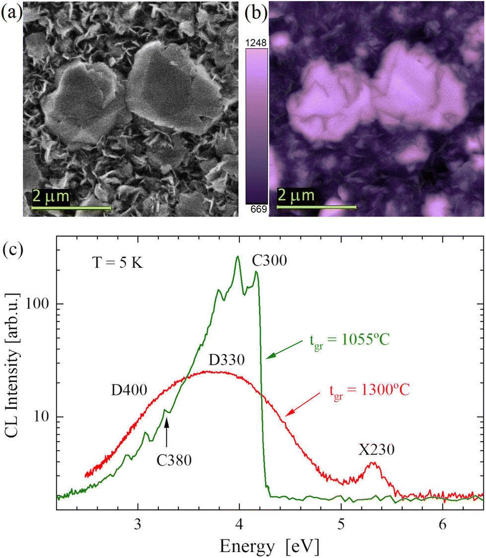 | ||
| Fig. 1 (a) Scanning electron microscopy image of a BN sample (grown at 1055 °C) and (b) its panchromatic CL map (current 0.02 nA). (c) The CL spectra of two MOVPE BN samples, grown at 1055 °C (e-beam current 2.7 nA) and 1300 °C (19.5 nA). | ||
The electron energy (2.5 keV) was high enough to excite bandgap emission. However, it was found that the near band-gap (range 5.8–6 eV) light was emitted only in a few points on the samples. In most of the cases, CL was emitted only at energies below 5.5 eV. Five characteristic luminescence bands observed in CL are labelled in Fig. 1c: X230, C300, D330, C380, and D400 have maxima at about 5.32 eV (233 nm), 4.16 eV (298 nm), 3.8 eV (330 nm), 3.26 eV (380 nm) and 3.1 eV (400 nm), respectively. It is worth noting that the C300 band (characteristic for samples grown at tgr below 1200 °C) was much brighter than emission from other centres. These bands will be discussed below, together with the results of PL spectroscopy.
The PL of samples grown at different temperatures, tgr, measured at 7 K, showed similar features to the CL spectra (see Fig. 2b). The photoluminescence excitation (PLE) spectra were recorded for the two most prominent peak series: C300 and C380. The PLE values were determined on the most intense PL lines in both series and the values were 3.95 eV, 3.04 eV, and 3.72 eV, for the C300, C380, and D330 emissions, respectively. A comparison of PL (excited at 5.8 eV) and PLE spectra are plotted in Fig. 2. The PLE amplitude is in arbitrary units since it is difficult to determine full emitted power; however, it is worth noting that luminescence was very efficient, comparable to good ZnO samples. It can be observed that for C300 and C380 bands (present in samples grown at tgr < 1200 °C) the zero phonon lines (ZPLs) are in the same position in PL and PLE spectra while phonon replicas are shifted. In the PL spectra the phonon replicas have lower energies and in the PLE spectra the phonon replicas have higher energies than the ZPLs, as expected. It can be noticed that photoexcitation at the energy of the C300 line also results in the excitation of the C380 lines. In the case of the D330 band (characteristic for samples grown at tgr > 1200 °C), the maxima of PL and PLE are shifted by about 0.4 eV. This energy shift is similar to the energy difference between the first phonon replicas in the PLE and PL spectra of the C300 and C380 bands. This suggests that the D330 band has a similar phonon structure to that of the C300 band and its ZPL is at 4.04 ± 0.05 eV.
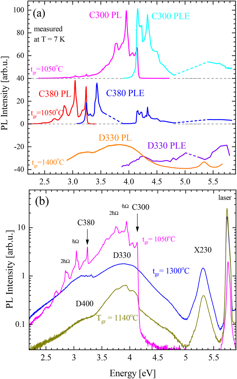 | ||
| Fig. 2 (a) Comparison of PL (red) and PLE (blue) spectra recorded for C380, C300 and D330 emissions, (b) PL spectra of h-BN samples grown at different temperatures, tgr, excited at 5.8 eV (215 nm), The C lines have sharp phonon replicas, ħΩ = 198 meV. | ||
The PLE spectra showed that the excitation was very effective for photons of about 5.8 eV, therefore, further PL measurements were made with a laser tuned to 5.8 eV. The representative PL spectra recorded on the samples grown at different temperatures are plotted in Fig. 2b. The peak of the highest energy, X230, was found at 5.4 eV (about 230 nm). Similar peaks in BN were reported as donor–acceptor pairs,35–37 bound excitons, or stacking faults.13,21,23 These peaks can have various energies due to locally different stacking orders.11,21 The energy of our peak at 5.3–5.4 eV is probably related to t-BN or r-BN (ABC) stacking.21
The samples grown at low temperatures have characteristic defects that emit light in the form of a few sharp peaks similarly to colour centres. The peaks are grouped in two bands C300 and C380. The C300 band consists of a ZPL at 4.144 eV (299 nm) and a few phonon replicas (the strongest one at 3.94 eV). The C380 band has a ZPL at 3.240 eV (383 nm). These peaks can be very sharp, showing a full width at half maximum (FWHM) of 7 meV (0.6 nm). The C300 peak was already reported in many publications.2,19–23 Initially, it has been proposed to be associated with carbon on the N site;2,20 however, later works25,27,28 suggest that it can be a carbon dimer, e.g. a complex of two carbons on N and B sites. In the case of C380, there is less information. A similar band was reported only by Era et al.2 at an energy of 3.208 eV with the conclusion that both CN and CB may play a role in this emission. In fact, the CNCB complex can have many configurations. In the closest configuration, the carbon atoms are direct neighbours, but carbon can also be on the opposite side of the same BN hexagon which may give rise to the structure observed as C380. The phonon replicas with a phonon of about 200 meV for both bands are in agreement with the calculated ab initio phonon modes.27,38
The samples grown at higher temperatures show broad emission (an FWHM of about 0.6 eV) bands D330 and D400, instead of the sharp bands C300 and C380. The D330 and D400 bands appear at energies of about 3.8 eV (330 nm) and about 3.1 eV (400 nm), respectively. In the work of Bourrellier et al.6 a band similar to D330 is visible in a plotted spectrum but not discussed. Similar spectra were also shown by Du et al.20 for samples obtained under a high NH3 flow and interpreted to be related to a carbon–nitrogen vacancy complex, similarly to C300 lines. The energetic positions of D330 and D400 suggest that they are somehow related to C300 and C380 lines. At first sight, they seem to be just the same emission lines but broadened. However, the emission energies of these bands can reach significantly higher values (500 meV or more) than the ZPL energies of the C bands. In the Discussion section, we propose to explain this effect by delocalization of the excited state and replacement of internal recombination by transitions from shallow donors.
The BN samples were grown with various thicknesses, different V/III ratios, and at different temperatures tgr. All of these parameters can influence the PL emission of the investigated samples. A comparison of the PL intensities of the samples with different thicknesses revealed almost no dependence on layers thicker than 300 nm. It can be explained by strong absorption in BN, where laser light penetrates only a depth of about 100–200 nm. It was directly observed that laser light (5.8 eV) is partially transmitted through the BN layer of less than 200 nm.
A correlation between the V/III ratio and peak intensities was also very weak. On the other hand, a clear correlation between the intensity and growth temperature was observed.
The intensities (signal at the maximum of a peak) of different PL bands measured in the investigated samples are plotted in Fig. 3. It can be observed that the PL intensity correlates with tgr. The C300 and C380 peak intensities strongly decrease, while those of X230 and D330 increase, with increasing tgr. The intensity of the D400 band is hard to quantify, and because this band is weak, it is not shown in this figure. However, it seems that the D400 intensity is positively correlated with tgr, similarly to D330.
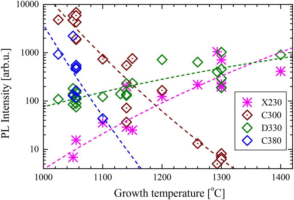 | ||
| Fig. 3 PL intensity of different emission bands (measured at 6 K), under 5.8 eV laser excitation energy, versus growth temperature. | ||
It is expected that the luminescence intensity should be proportional to the number of emitting centres but should decrease in the presence of nonradiative recombination defects. Usually, deep defects like colour centres are not disturbed by the presence of other defects, so only the high-energy exciton-related centres X230 should be quenched by nonradiative recombination. Therefore, the increase of the X230 intensity suggests a lower concentration of nonradiative centres when grown at higher growth temperatures, even if the observation of this band may still suggest the presence of stacking faults. The fast decrease of colour centres C300 and C380 intensities with an increase of tgr suggests that some processes activated at higher temperatures led to their annihilation. This can be either evaporation of the material or the creation of other defects that formed complexes with the original centres. We can assume that the intensity is described by the Arrhenius–Eyring equation:
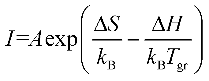 | (1) |
From the fitting procedure, we have also obtained the prefactor α = A![[thin space (1/6-em)]](https://www.rsc.org/images/entities/char_2009.gif) exp(ΔS/kB). For example, values of α were equal to 1.32 × 10⁻¹⁴ and 3.7 × 10⁻²³ for C300 and C380 centres, respectively. This means that at very high temperatures the formation of C380 would be 9 orders of magnitude less probable than C300, which means that the formation of C380-related defects is much more complex than in the case of C300.
exp(ΔS/kB). For example, values of α were equal to 1.32 × 10⁻¹⁴ and 3.7 × 10⁻²³ for C300 and C380 centres, respectively. This means that at very high temperatures the formation of C380 would be 9 orders of magnitude less probable than C300, which means that the formation of C380-related defects is much more complex than in the case of C300.
These data were obtained on samples grown in the simplest CFG mode (as described in the Growth of h-BN MOVPE layers section). Our group also developed other more elaborated modes, for example, flow modulation epitaxy (FME).24,39 In the FME mode it is possible to obtain emission similar to C300 at higher growth temperatures; however, lines are broader and shifted to lower energies (by 50–100 meV) compared to the CFG samples reported here.
The intensities of X230 and D330 emissions increase with the growth temperature, which suggests that these defects are more easily created at higher temperatures. In this case, H can be interpreted as the formation energy of a defect. The fitting of eqn (1) gave ΔH = (2.6 ± 0.3) eV and (1.1 ± 0.1) eV for X230 and D330 peaks, respectively. Theoretical calculations found the formation energy of the CBCN defect to be about 2 eV (ref. 25, 26 and 30) (the energy is positive since the original BBNN pair has a lower energy than the CBCN pair) and it is independent of nitrogen flux.
The C300 and C380 bands consist of a series of sharp lines. Time-resolved measurements show that these lines have nearly identical transients for each band, which suggests that they are phonon replicas. From theoretical calculations the optically active modes A2u, E1u(TO), and E1u(LO) are expected at energies 92.6 meV, 170.9 meV, and 199.7 meV, respectively.38,40,41
The comparison shown in Fig. 4 presents the spectra of C300 and C380 bands shifted by the energy of their zero-phonon transitions. It can be noticed that the phonon replicas of both bands are very similar and few phonon replicas can be identified. The phonon energy hΩ = 198 eV, (1600 cm−1) can be ascribed to E1u(LO), while the line observed at 171 meV (1380 cm−1) can be assigned to the E1u(TO) phonon. It should be noted that the E1u(TO) phonon energy is nearly the same as E2g, which dominates the Raman spectra. Similar replicas were reported in a few works22,23 for the C300 line, while the observation for the C380 line is new. The similarity of phonon replicas suggests that the C300 and C380 lines are closely related.
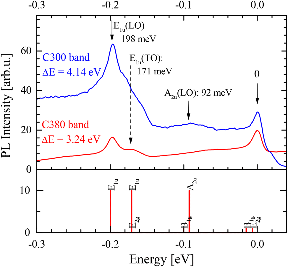 | ||
| Fig. 4 A comparison of phonon replica spectra (above) with theoretical predictions38 (below). The spectra are shifted by ΔE equal to zero phonon line energy. | ||
Time-resolved photoluminescence
PL is emitted by the radiative recombination of the excited states of density n(t). The evolution of this can be described by the rate equation: | (2) |
| n(t) = n(0)exp(−t/τ). | (3) |
In the case of feeding by another centre inside the sample (excited independently by a laser pulse at time tp) the feeding function can be assumed as an exponential decay (with lifetime τC): FC(t) = αexp(−t/τC), for t > 0 and FC(0) = 0, for t > 0. Incorporating this dependence in eqn (2), one obtains the solution:
| n(t) = Aexp(−t/τC) + Bexp(−t/τ), | (4) |
If the feeding function is a Gaussian pulse (excited by a laser) given by F(t) = ϕexp(−(t/w)2), then assuming the border condition n(−∞) = 0, the solution becomes:
 | (5) |
exp(−t/τC)exp((tD/w)2)/2 and tD = w2/2τ. While fitting to the experimental data, both D and tD were treated as fitting parameters.
A comparison of the time-resolved PL (TRPL) of low-tgr and high-tgr BN layers measured at low temperatures can be found in Fig. 5. The figures are presented as false-colour contour maps with subsequent contour lines plotted for values that are e-times smaller. Assuming that the measured PL intensity I(t) is exponential (proportional to n(t) from eqn (3)), the distance between the contour lines along the time axis is equal to the decay time τ (defined by eqn (2)), so the kinetics of the light emission can be easily determined. All spectral features have relatively long decay times – of the order of nanoseconds.
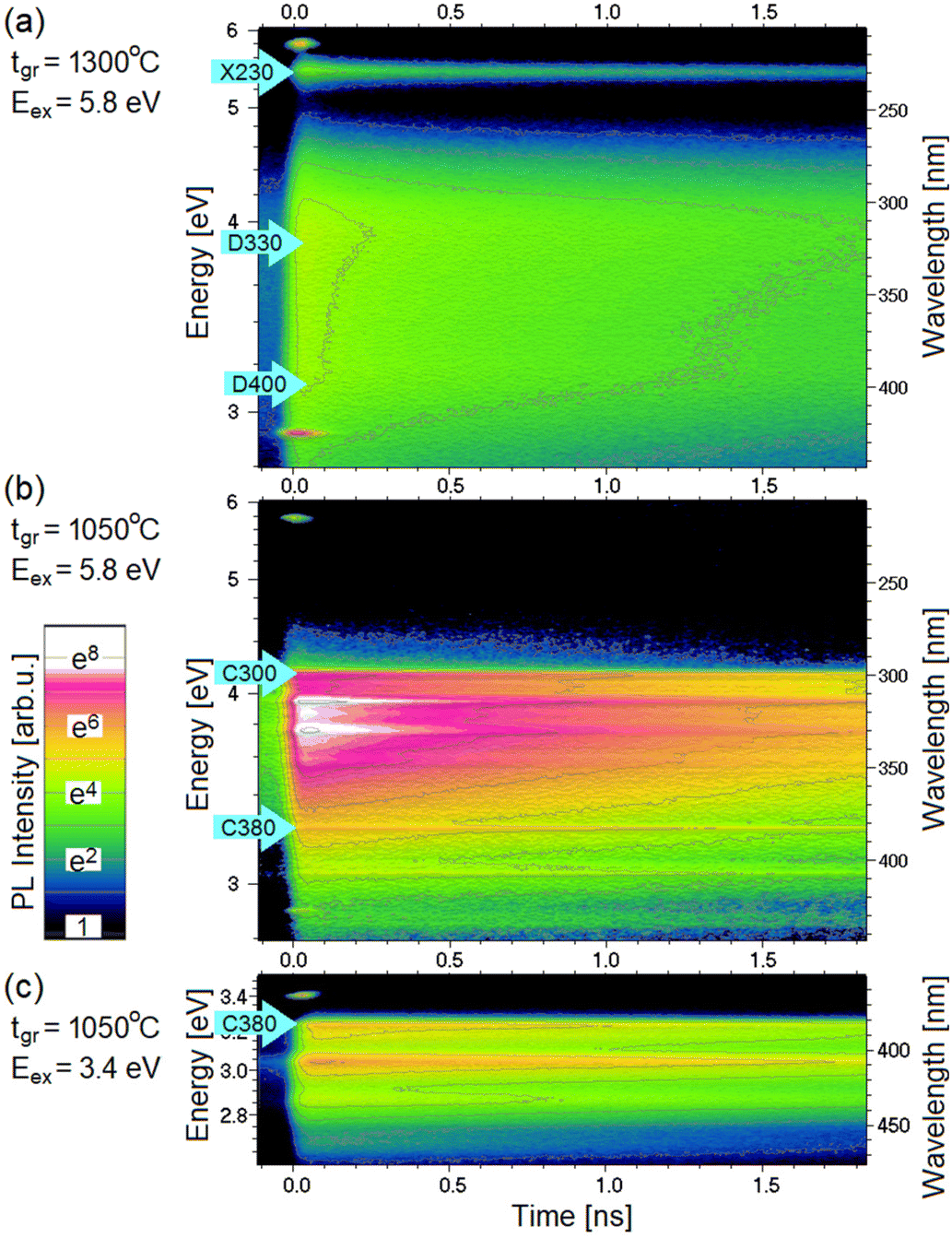 | ||
| Fig. 5 TRPL spectra of two BN samples: (a) a layer grown at a high temperature, bands X230 (at 5.4 eV), D330 (3.5–4 V) and D400 (3–3.2 eV) are visible, (b) a layer grown at a low temperature and excited at 5.8 eV (sharp C300 and C380 lines with ZPLs are at about 4.14 and 3.24 eV) and (c) low-temperature layer and excited at 3.4 eV (only C380). | ||
The luminescence evolution of a high growth temperature sample (excited at 5.8 eV) is plotted in Fig. 5a. As observed in CL (Fig. 2) and PL (Fig. 3b) such samples have significant emission from the X230, D330, and D400 bands. It can be observed that all emission bands have long lifetimes (the changes with time are small) except for the initial part (about 0.2 ns) where changes are visibly faster. An example of emission from a low-tgr sample excited at a high energy of 5.8 eV is plotted in Fig. 5b. As observed in CL and PL such a sample has no trace of the X230 emission but has well visible three lines of the C300 emission. A significant decrease in the amplitude with time reveals that the decay is fast. All three lines decay at the same rate. Three C380-related lines can be seen at 3.24 eV, 3.05 eV, and 2.95 eV. At t < 0.2 ns the C380 lines are hardly visible on the C300 background, but after 1.5 ns they emerge from this background. This observation proves that the C380 emission has a significantly longer lifetime than the C300 emission. A clear image of the C380 emission was obtained using 3.4 eV laser light, which does not excite the C300 band (see Fig. 5c).
PL transients of the characteristic bands of BN are plotted in Fig. 6a. The data were analysed by fitting theoretical curves described by eqn (3), (4), and (5). The simplest case was for the transient of the C380 peak excited at 3.4 eV. It was successfully fitted with the curve given by eqn (5). The obtained lifetime was τ = 1.7 ns, and the width w was about 0.03 ns. In the case of the X230, and D330 emission, their PL transients are two exponential, so it was necessary to fit the sum of two curves given by eqn (5) with different D and τ values but the same peak width w. In all cases, w was about 0.03 ns. The two lifetimes were assigned τS and τL for shorter and longer parts. Such an effect can be explained by the existence of two populations of centres: some of them are in the vicinity of the surface or defects, causing a faster recombination and others are not disturbed, therefore having longer lifetimes. These two lines can be fitted with a non-exponential curve also resulting from the theory of donor (D) to acceptor (A) recombination with various D–A distances.42 The C300 line can be fitted with a single exponential curve with τ = 0.9 ns or a two-exponential curve (τS = 0.4 ns and τL = 1.1 ns). The two-exponential curve gives a very nice fit (see Fig. 6a), but it has two more parameters.
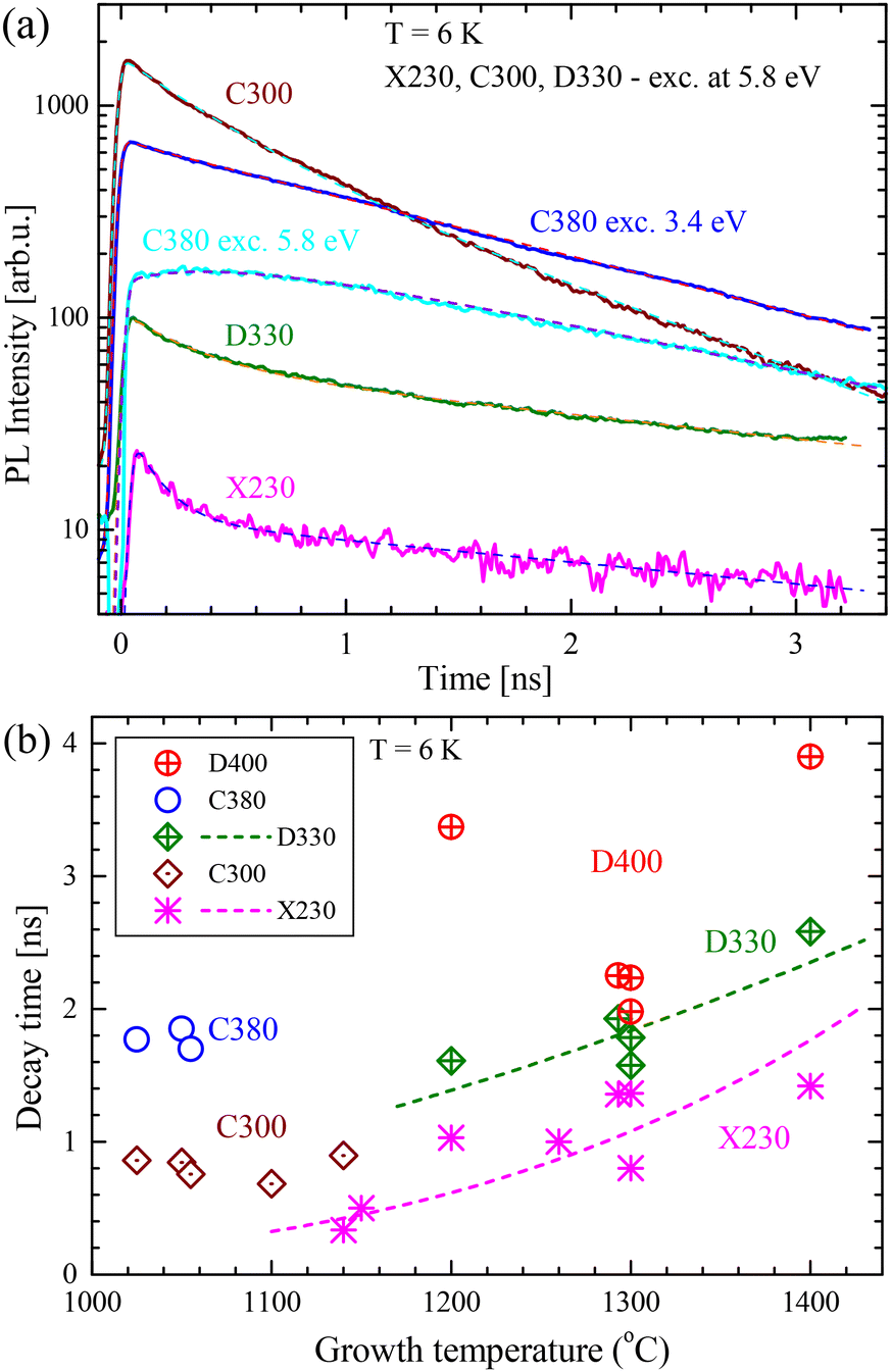 | ||
| Fig. 6 (a) PL transients of the characteristic PL bands (solid curves) with fitted curves (dashed curves). (b) Decay times of the main PL emission bands versus growth temperature. For the two exponential decays, the longer lifetimes have been plotted. The dashed curves are given by eqn (1). | ||
When comparing the C300 and C380 sharp lines, one finds significantly different lifetimes of about 0.9 ns and 1.8 ns, respectively. This difference is important since it proves that the C380 band is not a phonon replica of the C300 band. The C300 line lifetime has already been reported as 1.7 ns (ref. 2) and 1.1 ns.22 A line similar to C380 was reported only by Era et al.2 with a lifetime of 2 ns. Theoretical calculations predict a lifetime of 1.2 ns for the CBCN defect.25
As noticed in the PLE experiment, photoexcitation at the energy of the C300 line or above also results in the excitation of the C380 lines. Fig. 6a also shows the transient of the C380 line excited with 5.8 eV energy. A maximum of this transient is delayed related to the maximum of the C300 emission and C380 emission excited at 3.4 eV. This transient can be successfully fitted with the formula of eqn (4) that describes a transient caused by excitation from an exponentially decaying source. The source parameters were taken as equal to the C300 parameters. Additional pulse excitation was also assumed, which means that the C380 band was partially excited directly by the laser pulse and partially by the energy from the recombination of the C300 centres. It can be seen that the C380 band absorbs photons emitted by the C300 band or there is an excitation transfer from the C300 to C380 band.
The decay times obtained by the fitting of curves described by eqn (4) and (5) are plotted in Fig. 6b. In the case of two exponential decays, the time of the long-living part has been plotted. The lifetime of the high-energy X230 emission is generally longer in samples grown at higher tgr. This observation suggests a lower nonradiative recombination rate and thus higher sample quality for samples grown at about 1300 °C. The higher growth temperature most probably leads to a lower number of point defects that are nonradiative recombination centres. The X230 emission is probably due to stacking faults or other extended defects,13,21 so these results suggest that at high tgr, extended defects form instead of point defects. The data in Fig. 2b can be fitted by eqn (1) with activation enthalpy ΔH = (−1.1 ± 0.2) eV (dashed line in Fig. 6b).
In the case of the C300 band, the lifetimes are from 0.8 to 1 ns (0.9 ns on average). There is no clear dependence on the growth temperature. Such behaviour is expected, since electrons are strongly localized at these centres and are not sensitive to the influence of other defects. The D330 band has quite long lifetimes: 1.6–2.6 ns. The lifetime seems to increase with the growth temperature and an approximated dependence is plotted as a dashed line in Fig. 6b following eqn (1). The calculated enthalpy is ΔH = (−0.6 ± 0.2) eV. It can be noted that extrapolation of the D330 curve (below 1200 °C) also fits the data points for the C300 centre, which suggests some connection between these two centres. The D400 band has lifetimes in the range of 2–4 ns, which is significantly longer than those in the case of the C380 band (which has a similar energy to the D400 band).
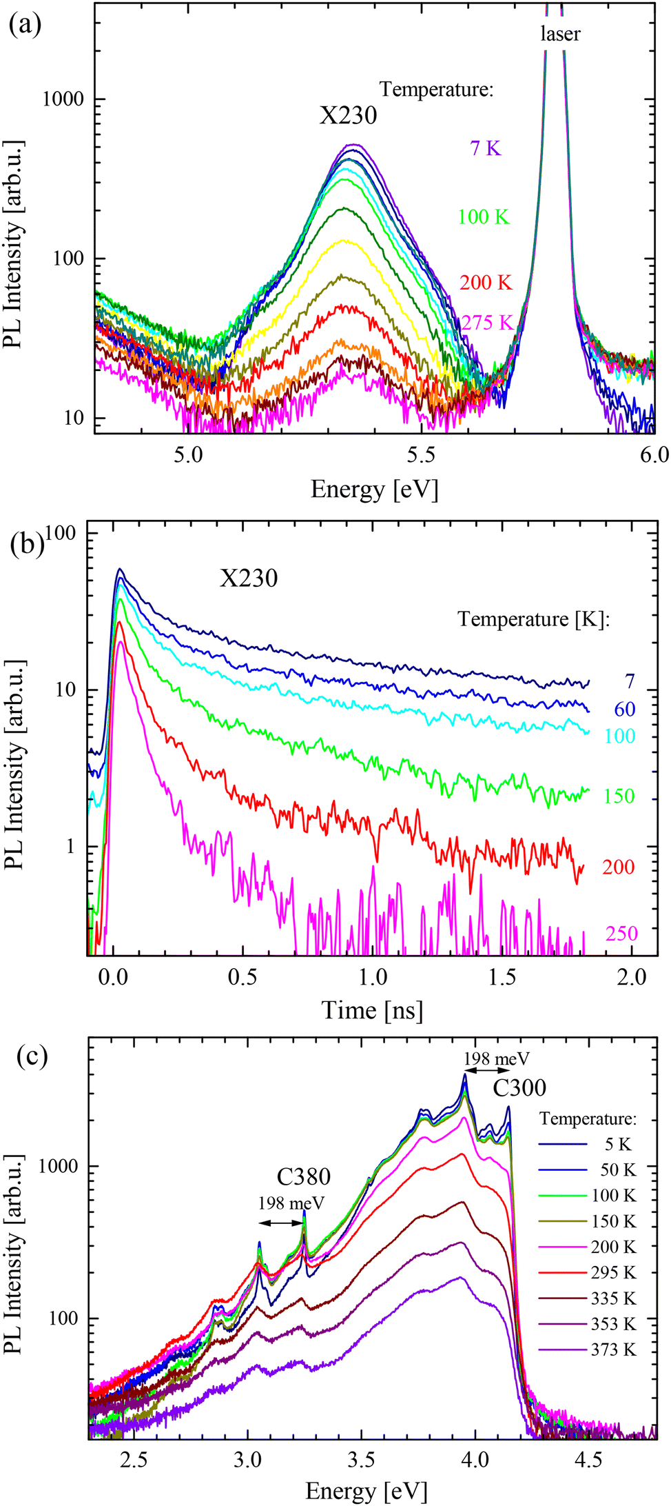
All of the above-mentioned luminescence bands were well visible also at room temperature, suggesting that the temperature dependence of luminescence was weak. The PL measurements as a function of temperature confirmed this observation.
The PL spectra for different measurement temperatures are plotted in Fig. 7 and it can be seen that energies of the PL peaks practically do not change with temperature. We can estimate that the shift between helium and room temperature of any peak is less than 15 meV. This is a small value compared to three-dimensional materials, for example, for GaAs this shift is 87 meV (ref. 43) and for GaN, it is 65 meV.44 For the X230 peak, an anomalous dependence – a decrease followed by an increase – has been revealed (Fig. 7a). A similar dependence was observed by Du et al.36 The C300 line energy is practically constant up to 380 K. We suppose that such a high thermal stability is due to a very small change of the h-BN lattice constant,45 similarly to the case of graphite. Chichibu et al. reported a similar low thermal dependence of the CL19 signal. This very weak thermal dependence of luminescence energy can be compared with anomalous phonon behaviour observed in BN. The E2glow phonon mode energy decreases with temperature, while the E2ghigh mode increases its energy.34,41 This effect is due to the thermal vibrations perpendicular to the BN plane that lead to the shrinkage of the BN lattice. Since the band gap depends on the lattice constant, the anomalous thermal lattice dependence36 causes anomalous energy dependence.
 | ||
| Fig. 7 PL spectra recorded at different temperatures: (a) a series of the X230 peak spectra, (b) PL transients of the X230 band, and (c) the C300 and C380 defect bands. | ||
The changes of PL intensity are also relatively small between helium and room temperature. The intensity decreases about 3 times. This means that the C300 and C380 emissions have a very high internal efficiency at room temperature.
The PL transients of the investigated defects measured at different temperatures are plotted in Fig. 7c. The decay times of deep defects C300, D330, C380 and D400 were nearly insensitive to temperature. The long lifetimes at room temperature indicated a very high internal efficiency of light emission. The X230 peak decay became faster with the increase of temperature. The thermal dependence of decay time could be fitted with the curve assuming a nonradiative process with thermal activation energy EA = 22 meV.
Discussion
The measurements focused on five types of emissions labelled X230, C300, C380, D330, and D400. The X230 emission shows different characteristics than the C and D defects and following other authors, we assume that it is most probably due to extended defects. In the case of C and D types of emissions, we propose that they are related to carbon impurities that are built in during growth. The carbon impurities are expected due to the use of B(C2H5)3 (TEB) molecules during the growth of BN. The presence of carbon was confirmed by our EDX measurements. In other reports, carbon was identified as the main impurity in h-BN from X-ray photoelectron spectroscopy (XPS).48 Some authors point also to other possible defects, for example, multi-carbon defects27,30 or a carbon-vacancy complex.49TEB and ammonia used as the precursors of boron and nitrogen atoms forming layers of h-BN can also react among themselves. There are numerous possible combinations of such reactions, and we selected the most plausible ones only. To this end, we analysed the stability of reactants and products for several potentially possible ways of replacement or decomposition reactions by using the ωB97XD functional46 with the def2-TZVP basis.47 The computations were performed with the G09 program.50 Some of the most probable reactions are plotted in Fig. 8. It turns out that there exists one exothermic reaction of the double replacement type:
| B(C2H5)3 + NH3 → B(C2H5)2NH2 + C2H6, ΔE = −1.27 eV, | (R1) |
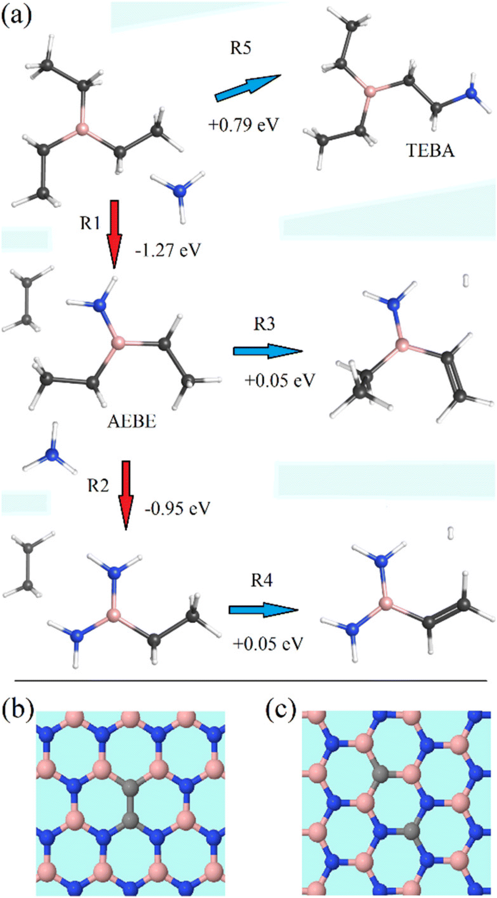 | ||
| Fig. 8 (a) The lowest energy TEB + NH3 reaction products, and two close configurations of C2 dimers in BN, (b) 1,2-CBCN, and (c) 1,4-CBCN, expected after build-in of C2 into BN. | ||
The reaction of this product with another ammonia molecule, leading to the replacement of the second ethyl group with the ammonia group, is also exothermic:
| B(C2H5)2NH2 + NH3 → B(C2H5)(NH2)2 + C2H6, ΔE = −0.95 eV. | (R2) |
Another reaction with AEBE results in the detachment of one hydrogen molecule leading to the formation of a chain of a boron atom and two carbon atoms connected with a double bond:
| B(C2H5)2NH2 → B(C2H5)(C2H3)NH2 + H2, ΔE = +0.05 eV. | (R3) |
A similar detachment with the same energetics is predicted for the product of (R2):
| B(C2H5)(NH2)2 → B(C2H3)(NH2)2 + H2, ΔE = +0.05 eV. | (R4) |
Therefore, one can expect the presence of these molecules during the growth of the h-BN layer, which can lead to a modification of the desired product (e.g. the ethylene group present in the reactions (R3) and (R4) can be built into the forming h-BN framework, creating the CBCN defect). Other reactions of TEB with ammonia are endothermic, but some of them need only small energy, like:
| TEB + NH3 → B(C2H5)2C2H5NH2 + H2, ΔE = +0.79 eV. | (R5) |
While searching for reaction paths and barriers, we preliminarily located the saddle points with the ORCA program51 using a B97-3c52 composite method in the def2-SVP basis set, and then we reoptimized the configurations with Gaussian with the same method as used for the minimal energy of the molecule configurations.
The possible mechanism of the (R1) reaction is a two-step process: the first step is barrierless and involves the attraction and attachment of ammonia to TEB, giving rise to a TEB–NH3 complex with tetracoordinated boron, which is 0.47 eV more stable than the reagents. The second step, which is performed by a concerted elongation of the C–B bond and the donation of a hydrogen molecule from the complexed ammonia, has a barrier of 1.47 eV with respect to the TEB–NH3 complex.
Similarly, a two-step process can be proposed for the (R2) reaction. In the first step, an attachment of the ammonia molecule to AEBE takes place (in this case the complex lies, however, a little bit – of 0.13 eV – higher than reactants), and in the second step, the ethane molecule is separated from the complex by taking an extra hydrogen molecule from the complexed ammonia with a reaction barrier of 1.62 eV.
We can conclude that the reactions are thermodynamically possible under the conditions in a reactor, at temperatures above 1000 °C.
Calculations of the thermodynamics of carbon defects show that the formation energy of single carbon in BN is much higher than the formation energy of CBCN, so whenever carbon is present during the growth of h-BN, a pair of carbons should be a common defect.25 Based on ab initio emission energy calculations27 the most probable explanation for the C300 defect is the carbon dimer in the shape of two closest boron and nitride substitutions 1,2-CBCN (see Fig. 8b). Such a defect can be caused by partial incorporation of AEBE (reaction (R1), Fig. 8a). This configuration is the simplest and most tightly bound. Similar identification was proposed in other reports too.14,25,26,28,53 We think that it is the most probable identification; however, other propositions were also published, for example, a single CN defect2,6,48 or a CN–VN complex.20
The C380 defect has a slightly lower energy than C300, but it has a similar dependence on the growth temperature and a similar PL lifetime to C300, so it has probably a similar origin to C300. We propose that the C380 defect may also be formed by two carbon atoms in boron and nitrogen positions; however, not by the next neighbours, but by a 1,4-CBCN defect for which two carbon atoms are at the opposite sides of a BN hexagon (see Fig. 8c). Moreover, the expected energy of the 1,4-CBCN defect was calculated to be about 1 eV lower than the 1,2-CBCN defect,27 which fits well to the C300–C380 energy difference. Such a defect can be caused by the partial incorporation of TEBA (reaction (R5), Fig. 8a). However, there are a lot of other possible configurations of carbon defects that could be related to the plethora of lines observed in BN at lower energies.27,29
In samples grown at high temperatures (tgr > 1200 °C) the lines related to the colour centres are replaced by broad defect bands D330 and D400 (width of about 1 eV). These bands have similar central energies but they extend over a large energy range. It can happen that the similarity of energies is accidental and C and D centres have different chemical origin. However, such hypothesis is the least interesting one.
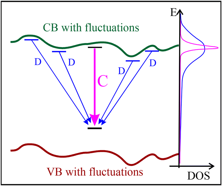
We propose (see Fig. 9) that C bands are internal transitions of some localized centres CX → C0, while D bands emerge from transitions between external donors Dex and the localized centres responsible for the C lines, Dex → C0. The sharp lines are direct in real space. Broad bands come from the recombination between two distant centres, so they are strongly influenced by potential fluctuations. The potential fluctuations would change the energy randomly, making the line much broader. The recombination over a long distance is possible for centres with a large radius of the wave function, which means that it occurs for shallow centres. This hypothesis proposes that the final state is the same. The final state has a low energy, so its wave function is localized and not very sensitive to changes of the crystal structure. If the ground state is the same for C and D transitions, it is enough to assume that the energy of the excited state CX is very close to the conduction band minimum, in order to explain why the energies of the D-band are similar to the C lines. However, it is not clear why the excited state has an energy similar to the conduction band energy and why the localized excited states vanish in samples grown at high temperatures. A few hypotheses are possible:
The first explanation would assume that at higher temperatures, samples have less donor defects, so the Fermi level is low. If the Fermi level were low, the ground state in the dark would be empty, so no internal excitation would be expected. The CBCN+/0 ionization level was calculated to be about 0.8 eV above the valence band,25 which means that the ionization hypothesis is quite probable. However, this hypothesis does not explain why the excited state has an energy similar to the conduction band energy.
 | ||
| Fig. 9 Scheme of the transition explaining the emission of the C and D bands. | ||
The second hypothesis suggests that the C300–>D330 transformation is due to natural defects or even cubic BN (c-BN), since it was published that it is the most stable phase of BN below 1392 °C.54 Our XRD measurements (as well as Raman and IR spectroscopy24,34) did not show the c-BN phase; however, the peaks are very broad and we cannot exclude the nanocrystals of c-BN. So it may be that the sharp lines are from c-BN, but since such lines were observed also in samples that are of pure h-BN,4 this hypothesis has low probability. Moreover, as shown in Fig. 4, the C300 and C380 lines have a spectrum of phonon replicas exactly matching the h-BN phonon density. But some imperfection can be involved in the origin of these lines which leads to the third hypothesis.
The third and in our opinion the most probable hypothesis is based on a strongly disordered, turbostratic (t-BN) structure of samples grown at low temperatures. In such structures the flakes of BN are twisted and positioned nearly randomly. Instead of AA′ or AB configuration one can expect different angles of layer-to-layer alignment leading to moiré-like effects. In such situations, boron atoms of one BN layer can be placed above the boron atoms of other BN layers. Such stacking would cause repulsion of layers. The BN layers could not stack exactly one above another, so one can expect even voids between flakes or at least a weaker interaction between the BN layers. Similar decoupling was observed in graphene.55 It could happen that there exists an excited state that is localized in a single layer of BN and it becomes degenerate with the conduction band in the bulk material, so it vanishes when BN is well ordered. This hypothesis naturally explains why at a higher temperature, with a better BN structure, the sharp lines vanish and are replaced by a broad band with similar energy.
The influence of neighbouring layers has some support in the literature,56,57 for example, Du et al.57 noticed that exfoliation changes the BN band gap and can influence the donor–acceptor recombination. Based on cathodoluminescence and high-resolution transmission electron microscopy, it was reported lately58 that twisted BN flakes emit strongly in the UV region (stronger than aligned flakes). Theoretically, the influence of neighbouring flakes on defects was studied in works.14,28
In ref. 14 a theoretical study of the influence of the second layer on the properties of various defects, including the dicarbon defect, has been performed using the time-dependent density-functional theory (TD-DFT) with a functional based on the CAM-B3PLYP functional59 (for details, see the reference above). Using the same transition density matrices (TDMs), as obtained in this paper and utilizing the methodology of Plasser and Lischka,60 we performed a more detailed analysis of the character of the first excited state, which for the case of the AA′ bilayer has an excitation energy of 4.88 eV for a bilayer of two clusters: one with the 1,2-CBCN defect and another without any defect, see Fig. 10a. If atoms of this species are divided into three sets: (1) “defect”, i.e. both carbon atoms and four adjacent B and N atoms, (2) “wrapper”: the remaining atoms of the same layer, and (3) “sheet2”: all the atoms from the second layer, then the electron–hole correlation plot for this state looks like that presented in Fig. 10. It is clearly seen that although the main part of the excitation remains within the defect and its close environment, there is a relatively large “defect”-to-“sheet2” contribution (top-left element of the plot), which is responsible for the charge-transfer effect from the defect to the second layer.
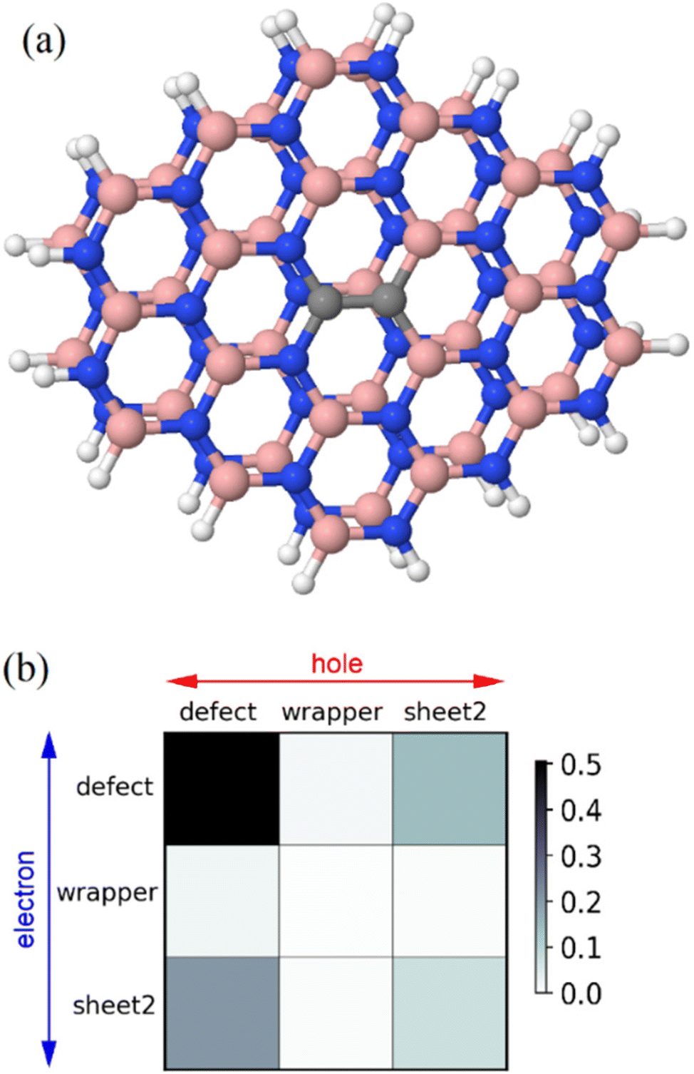 | ||
| Fig. 10 (a) The bilayer model with the 1,2-CBCN defect and (b) the electron–hole correlation diagram for the first excited state of this model (the darker cell of the diagram – the higher transition density). | ||
Since disorder in the turbostratic material creates many shifts in layering resulting in partial decoupling of layers where the interaction between the BN layers may be weak, it can happen that the excited state exists in its localized form only in such circumstances. In the ordered material, grown at a high temperature, the influence of neighbouring layers leads to delocalization of the excited state, so the C300 and C380 lines vanish and are replaced by delocalized transitions D (Fig. 9). The assumption of the nearly-degenerate state also explains why the excited state has the energy similar to the conduction band energy.
Conclusions
The luminescence of MOVPE grown hexagonal BN has been measured in the ultraviolet (PL up to 5.8 eV, CL up to 7.7 eV) range and several defect-related emission bands have been observed and analysed. The brightest band is observed at about 300 nm (marked C300, with a zero-phonon line, ZPL, at 4.14 eV) and is composed of several strong lines. We have also found a similar band consisting of multiple sharp lines with a ZPL at 3.24 eV, labelled as C380. Due to these narrow lines, the emission is similar to the color centres observed in other wide band-gap materials. We propose that the C300 and C380 lines are related to 1,2-CBCN and 1,4-CBCN defects, respectively. The C300 lines are the brightest ones but are somehow mysterious since they vanish in the high-tgr samples. It means they are absent in samples that have better structural properties as revealed by XRD and SEM and they are present mainly in samples grown at low temperatures (tgr < 1200 °C). We have found that in samples grown at higher temperatures the lines related to colour centres are replaced by broad defect bands D330 and D400 (widths of about 1 eV). The C lines are most probably the internal transition of carbon-related defects. The D bands have similar central energies to C bands but a vastly extended energy range, so we propose that the D bands are due to the recombination from some shallow defects to the deep ground state of the CNCB defect. The transition from sharp to broad lines is due to the delocalization of the excited states of the CNCB defect caused by the close alignment of BN layers in a material with a well-ordered structure.The lifetimes of luminescence bands in different BN samples have been determined in the range from 0.03 ns (X230), 0.9 ns (C300), 1.8 ns (C380) to 4 ns (D400). The X230 and D330 lifetimes increase with the growth temperature, which indicates lower nonradiative recombination and a better structure of the high-temperature BN layers.
The temperature dependence of luminescence energy is rather weak. Up to room temperature the peak position of the excitonic emission X230 changes only by 15 meV and for the C and D lines almost no change is observed. So the high thermal stability is due to a very small change of the h-BN lattice constant. The long lifetimes at room temperature indicate a very high internal efficiency of light emission.
The colour centre luminescence and its dependence on the growth temperature (revealed by our research) are one of the fundamental properties that have to be understood for future applications. Our work shows that by changing the growth temperature one can strongly influence the emission spectrum of deep defects, which shows that defect properties are tuneable in MOVPE grown BN. If our hypotheses are correct these lines can serve as markers for carbon content and can also be important for different applications. For example, in optoelectronics, such bright lines can be used in LEDs and also in devices based on single photon emitters6 or spin effects, and in neutron detectors,8 these lines can be efficient scintillators.
Author contributions
K.P.K. – measurements, analysis, and coordination. J.B., A.R. and M.T. – measurements and analysis. A.K.D. and J.I. – sample growth and characterization. T.K. – theoretical calculations. R.S. and A.W. – data analysis and funding acquisition. All authors contributed to writing and discussed the manuscript. All authors have read and approved the manuscript.Conflicts of interest
There are no conflicts to declare.Acknowledgements
We are grateful to late Krzysztof Pakuła for sample growth and discussions. This work was partially supported by the National Science Centre grants no. 2019/33/B/ST5/02766 and 2020/39/D/ST7/02811. The theoretical part of this research was partially supported by PL-Grid Infrastructure.References
- G. Cassabois, P. Valvin and B. Gil, Hexagonal boron nitride is an indirect bandgap semiconductor, Nat. Photonics, 2016, 10, 262 CrossRef CAS.
- K. Era, F. Minami and T. Kuzuba, Fast luminescence from carbon-related defects of hexagonal boron nitride, J. Lumin., 1981, 24–25, 71 CrossRef CAS.
- L. Schue, L. Sponza, A. Plaud, H. Bensalah, K. Watanabe, T. Taniguchi, F. Ducastelle, A. Loiseau and J. Barjon, Bright Luminescence from Indirect and Strongly Bound Excitons in h-BN, Phys. Rev. Lett., 2019, 122, 067401 CrossRef CAS PubMed.
- K. Watanabe and T. Taniguchi, Int. J. Appl. Ceram. Technol., 2011, 8, 977–989, DOI:10.1111/j.1744-7402.2011.02626.x.
- Su.-B. Song, S. Yoon, So Y. Kim, S. Yang, S.-Y. Seo, S. Cha, H.-W. Jeong, K. Watanabe, T. Taniguchi, G.-Ho Lee, J. S. Kim, M.-Ho Jo and J. Kim, Deep-ultraviolet electroluminescence and photocurrent generation in graphene/h-BN/graphene heterostructures, Nat. Commun., 2021, 12, 7134, DOI:10.1038/s41467-021-27524-w.
- R. Bourrellier, S. Meuret, A. Tararan, O. Stéphan, M. Kociak, L. H. G. Tizei and A. Zobelli, Bright UV Single Photon Emission at Point Defects in h-BN, Nano Lett., 2016, 16, 4317–4321, DOI:10.1021/acs.nanolett.6b01368.
- N. Mendelson, D. Chugh, J. R. Reimers, T. S. Cheng, A. Gottscholl, H. Long, C. J. Mellor, A. Zettl, V. Dyakonov, P. H. Beton, S. V. Novikov, C. Jagadish, H. H. Tan, M. J. Ford, M. Toth, C. Bradac and I. Aharonovich, Identifying carbon as the source of visible single-photon emission from hexagonal boron nitride, Nat. Mater., 2021, 20, 321 CrossRef CAS PubMed.
- T. C. Doan, S. Majety, S. Grenadier, J. Li, J. Y. Lin and H. X. Jiang, Fabrication and characterization of solid-state thermal neutron detectors based on hexagonal boron nitride epilayers, Nucl. Instrum. Methods Phys. Res., Sect. A, 2014, 748, 84, DOI:10.1016/j.nima.2014.02.031.
- J. Binder, A. K. Dabrowska, M. Tokarczyk, K. Ludwiczak, R. G. Kowalski, R. Stepniewski and A. Wysmolek, Epitaxial hexagonal boron nitride for hydrogen generation by radiolysis of interfacial water, Nano Lett. , 2023, 23, 1267–1272, DOI:10.1021/acs.nanolett.2c04434.
- V. Yadav and V. Kulshrestha, Boron nitride: a promising material for proton exchange membranes for energy applications, Nanoscale, 2019, 11, 12755 RSC.
- M. Moret, A. Rousseau, P. Valvin, S. Sharma, L. Souqui, H. Pedersen, H. Högberg, G. Cassabois, J. Li, J. H. Edgar and B. Gil, Rhombohedral and turbostratic boron nitride: X-ray diffraction and photoluminescence signatures, Appl. Phys. Lett., 2021, 119, 262102, DOI:10.1063/5.0076424.
- L. Sponza, H. Amara, C. Attaccalite, S. Latil, T. Galvani, F. Paleari, L. Wirtz and F. Ducastelle, Direct and indirect excitons in boron nitride polymorphs: A story of atomic configuration and electronic correlation, Phys. Rev. B, 2018, 98, 125206 CrossRef CAS.
- A. Rousseau, M. Moret, P. Valvin, W. Desrat, J. Li, E. Janzen, L. Xue, J. H. Edgar, G. Cassabois and B. Gil, Determination of the optical bandgap of the Bernal and rhombohedral boron nitride polymorphs, Phys. Rev. Mater., 2021, 5, 064602, DOI:10.1103/PhysRevMaterials.5.064602.
- M. Chojecki, E. Lewandowska and T. Korona, Influence of the second layer on geometry and spectral properties of doped two-dimensional hexagonal boron nitride, J. Mol. Model., 2020, 26, 216, DOI:10.1007/s00894-020-04456-8.
- A. Zunger, A. Katzir and A. Halperin, Optical properties of hexagonal boron nitride, Phys. Rev. B: Solid State, 1976, 13, 5560 CrossRef CAS.
- K. Watanabe, T. Taniguchi and H. Kanda, Direct-bandgap properties and evidence for ultraviolet lasing of hexagonal boron nitride single crystal., Nat. Mater., 2004, 3, 404–409, DOI:10.1038/nmat1134.
- C. Elias, P. Valvin, T. Pelini, A. Summerfield, C. J. Mellor, T. S. Cheng, L. Eaves, C. T. Foxon, P. H. Beton, S. V. Novikov, B. Gil and G. Cassabois, Direct band-gap crossover in epitaxial monolayer boron nitride, Nat. Commun., 2019, 10, 2639, DOI:10.1038/s41467-019-10610-5.
- C. Elias, G. Fugallo, P. Valvin, C. L'Henoret, J. Li, J. H. Edgar, F. Sottile, M. Lazzeri, A. Ouerghi, B. Gil and G. Cassabois, Flat Bands and Giant Light-Matter Interaction in Hexagonal Boron Nitride, Phys. Rev. Lett., 2021, 127, 137401 CrossRef CAS PubMed.
- S. F. Chichibu, Y. Ishikawa, H. Kominami and K. Hara, Nearly temperature-independent ultraviolet light emission intensity of indirect excitons in hexagonal BN microcrystals, J. Appl. Phys., 2018, 123, 065104 CrossRef.
- X. Z. Du, J. Li, J. Y. Lin and H. X. Jiang, The origin of deep-level impurity transitions in hexagonal boron nitride, Appl. Phys. Lett.J. Appl. Phys., 2015, 106, 021110 CrossRef.
- R. Bourrellier, M. Amato, L. H. G. Tizei, Ch. Giorgetti, A. Gloter, M. I. Heggie, K. March, O. Stephan, L. Reining, M. Kociak and A. Zobelli, Nanometric Resolved Luminescence in h-BN Flakes: Excitons and Stacking Order, ACS Photonics, 2014, 1, 857–862, DOI:10.1021/ph500141j.
- L. Museur, E. Feldbach and A. Kanaev, Defect-related photoluminescence of hexagonal boron nitride, Phys. Rev. B: Condens. Matter Mater. Phys., 2008, 78, 155204 CrossRef.
- T. Q. P. Vuong, G. Cassabois, P. Valvin, A. Ouerghi, Y. Chassagneux, C. Voisin and B. Gil, Phonon-Photon Mapping in a Color Centre in Hexagonal Boron Nitride, Phys. Rev. Lett., 2016, 117, 097402, DOI:10.1103/PhysRevLett.117.097402.
- A. K. Dąbrowska, M. Tokarczyk, G. Kowalski, J. Binder, R. Bozek, J. Borysiuk, R. Stępniewski and A. Wysmołek, Two stage epitaxial growth of wafer-size multilayer h-BN by metal-organic vapor phase epitaxy – a homoepitaxial approach, 2D Mater., 2021, 8, 015017, DOI:10.1088/2053-1583/abbd1f.
- M. Mackoit-Sinkeviciene, M. Maciaszek, C. G. Van de Walle and A. Alkauskas, Carbon dimer defect as a source of the 4.1 eV luminescence in hexagonal boron nitride, Appl. Phys. Lett., 2019, 115, 212101, DOI:10.1063/1.5124153.
- M. Maciaszek, L. Razinkovas and A. Alkauskas, Thermodynamics of carbon point defects in hexagonal boron nitride, Phys. Rev. Mater., 2022, 6, 014005 CrossRef CAS.
- T. Korona and M. Chojecki, Int. J. Quantum Chem., 2019, 119, e25925, DOI:10.1002/qua.25925.
- M. Winter, M. H. E. Bousquet, D. Jacquemin, I. Duchemin and X. Blase, Photoluminescent properties of the carbon-dimer defect in hexagonal boron-nitride: A many-body finite-size cluster approach, Phys. Rev. Mater., 2021, 5, 095201 CrossRef CAS.
- P. Auburger and A. Gali, Towards ab initio identification of paramagnetic substitutional carbon defects in hexagonal boron nitride acting as quantum bits, Phys. Rev. B, 2021, 104, 075410 CrossRef CAS.
- P. Huang, M. Grzeszczyk, K. Vaklinova, K. Watanabe, T. Taniguchi, K. S. Novoselov and M. Koperski, Carbon and vacancy centers in hexagonal boron nitride, Phys. Rev. B, 2022, 106, 014107 CrossRef CAS.
- O. L. Krivanek, M. F. Chisholm, V. Nicolosi, T. J. Pennycook, G. J. Corbin, N. Dellby, M. F. Murfitt, C. S. Own, Z. S. Szilagyi, M. P. Oxley, S. T. Pantelides and S. J. Pennycook, Atom-by-atom structural and chemical analysis by annular dark-field electron microscopy, Nature, 2010, 464, 571–574, DOI:10.1038/nature08879.
- A. K. Dąbrowska, K. Pakuła, R. Bożek, J.-G. Rousset, D. Ziółkowska, K. Gołasa, K. P. Korona, A. Wysmołek and R. Stępniewski, Structural and Optical Properties of Boron Nitride Grown by MOVPE, Acta Phys. Pol., A, 2016, 129, A129, DOI:10.12693/APhysPolA.129.A-129.
- K. Pakuła, A. Dąbrowska, M. Tokarczyk, R. Bożek, J. Binder, G. Kowalski, A. Wysmołek and R. Stępniewski, DOI:10.48550/arXiv.1906.05319.
- J. Iwanski, P. Tatarczak, M. Tokarczyk, A. K. Dąbrowska, J. Pawłowski, J. Binder, G. Kowalski, R. Stępniewski and A. Wysmołek, Temperature induced giant shift of phonon energy in epitaxial boron nitride layers, Nanotechnology, 2023, 34, 015202 CrossRef PubMed.
- L. Schué, I. Stenger, F. Fossard, A. Loiseau and J. Barjon, Characterization methods dedicated to nanometer-thick h-BN layers, 2D Mater., 2017, 4, 015028 CrossRef.
- X. Z. Du, J. Li, J. Y. Lin and H. X. Jiang, Temperature dependence of the energy bandgap of multi-layer hexagonal boron nitride, Appl. Phys. Lett., 2017, 111, 132106, DOI:10.1063/1.4994070.
- L. Museur and A. V. Kanaev, Near band-gap photoluminescence properties of hexagonal boron nitride, J. Appl. Phys., 2008, 103, 103520 CrossRef.
- J. Serrano, A. Bosak, R. Arenal, M. Krisch, K. Watanabe, T. Taniguchi, H. Kanda, A. Rubio and L. Wirtz, Vibrational Properties of Hexagonal Boron Nitride: Inelastic X-Ray Scattering and Ab Initio Calculations, Phys. Rev. Lett., 2007, 98, 095503 CrossRef CAS PubMed.
- Y. Kobayashi, T. Akasaka and T. Makimoto, Hexagonal boron nitride grown by MOVPE, J. Cryst. Growth, 2008, 310, 5048, DOI:10.1016/j.jcrysgro.2008.07.057.
- R. Geick, C. H. Perry and G. Rupprecht, Phys. Rev., 1966, 146, 543 CrossRef CAS.
- R. Cusco, B. Gil, G. Cassabois and L. Artus, Temperature dependence of Raman-active phonons and anharmonic interactions in layered hexagonal BN, Phys. Rev. B, 2016, 94, 155435 CrossRef.
- D. G. Thomas, J. J. Hopfield and M. Augustyniak, Kinetics of Radiative Recombination at Randomly Distributed Donors and Acceptors, Phys. Rev., 1965, 140, A202–A220, DOI:10.1103/PhysRev.140.A202.
- M. B. Panish and H. C. Casey Jr., Temperature Dependence of the Energy Gap in GaAs and GaP, J. Appl. Phys., 1969, 40, 163, DOI:10.1063/1.1657024.
- K. P. Korona, A. Wysmolek, K. Pakula, R. Stepniewski, J. M. Baranowski, I. Grzegory, B. Lucznik, M. Wróblewski and S. Porowski, Exciton Region Reflectance of Homoepitaxial GaN Layers, Appl. Phys. Lett., 1996, 69, 788, DOI:10.1063/1.117892.
- B. Yates, M. J. Overy and O. Pirgon, Philos. Mag., 1975, 32, 847 CrossRef CAS.
- J.-D. Chai and M. Head-Gordon, Long-range corrected hybrid density functionals with damped atom-atom dispersion corrections, Phys. Chem. Chem. Phys., 2008, 10, 6615 RSC.
- F. Weigend and R. Ahlrichs, Balanced Basis Sets of Split Valence, Triple Zeta Valence and Quadruple Zeta Valence Quality for H to Rn: Design and Assessment of Accuracy, Phys. Chem. Chem. Phys., 2005, 7, 3297–3305, 10.1039/b508541a.
- D. Chugh, J. Wong-Leung, L. Li, M. Lysevych, H. H. Tan and C. Jagadish, Flow modulation epitaxy of hexagonal boron nitride, 2D Mater., 2018, 5, 045018 CrossRef CAS.
- S. Li and A. Gali, Bistable carbon-vacancy defects in h-BN, Front. Quantum. Sci. Technol., 2022, 1, 1007756, DOI:10.3389/frqst.2022.1007756.
- M. J. Frisch, G. W. Trucks, H. B. Schlegel, G. E. Scuseria, M. A. Robb, J. R. Cheeseman, G. Scalmani, V. Barone, B. Mennucci, G. A. Petersson, H. Nakatsuji, M. Caricato, X. Li, H. P. Hratchian, A. F. Izmaylov, J. Bloino, G. Zheng, J. L. Sonnenberg, M. Hada, M. Ehara, K. Toyota, R. Fukuda, J. Hasegawa, M. Ishida, T. Nakajima, Y. Honda, O. Kitao, H. Nakai, T. Vreven, J. A. Montgomery, J. E. Peralta, F. Ogliaro, M. Bearpark, J. J. Heyd, E. Brothers, K. N. Kudin, V. N. Staroverov, R. Kobayashi, J. Normand, K. Raghavachari, A. Rendell, J. C. Burant, S. S. Iyengar, J. Tomasi, M. Cossi, N. Rega, J. M. Millam, M. Klene, J. E. Knox, J. B. Cross, V. Bakken, C. Adamo, J. Jaramillo, R. Gomperts, R. E. Stratmann, O. Yazyev, A. J. Austin, R. Cammi, C. Pomelli, J. W. Ochterski, R. L. Martin, K. Morokuma, V. G. Zakrzewski, G. A. Voth, P. Salvador, J. J. Dannenberg, S. Dapprich, A. D. Daniels, O. Farkas, J. B. Foresman, J. V. Ortiz, J. Cioslowski and D. J. Fox, Gaussian∼09 A.1, Gaussian Inc., Wallingford CT, 2009 Search PubMed.
- F. Neese, Software update: the ORCA program system, version 4.0, Wiley Interdiscip. Rev.: Comput. Mol. Sci., 2018, 8, e1327 Search PubMed.
- J. G. Brandenburg, C. Bannwarth, A. Hansen and S. Grimme, B97–3c: A revised low-cost variant of the B97-D density functional method, J. Chem. Phys., 2018, 148, 064104, DOI:10.1063/1.5012601.
- T. Korona, J. Jankowska and E. Masoumifeshani, Dicarbon defect in hexagonal boron nitride monolayer – a theoretical study, Can. J. Chem., 2023 DOI:10.1139/cjc-2022-0291.
- V. L. Solozhenko and V. Z. Turkevich, Phase Diagram of the B–BN System at Pressures up to 24 GPa: Experimental Study and Thermodynamic Analysis, J. Phys. Chem. C, 2018, 122, 8505–8509 CrossRef CAS.
- C. Faugeras, J. Binder, A. A. L. Nicolet, P. Leszczynski, P. Kossacki, A. Wysmolek, M. Orlita and M. Potemski, A micro-magneto-Raman scattering study of graphene on a bulk graphite substrate, Europhys. Lett., 2014, 108, 27011, DOI:10.1209/0295-5075/108/27011.
- A. Rousseau, P. Valvin, C. Elias, L. Xue, J. Li, J. H. Edgar, B. Gil and G. Cassabois, Stacking-dependent deep level emission in boron nitride, Phys. Rev. Mater., 2022, 6, 094009 CrossRef CAS.
- X. Z. Du, M. R. Uddin, J. Li, J. Y. Lin and H. X. Jiang, Layer number dependent optical properties of multilayer hexagonal BN epilayers, Appl. Phys. Lett., 2017, 110, 092102, DOI:10.1063/1.4977425.
- C. Su, F. Zhang, S. Kahn, B. Shevitski, J. Jiang, C. Dai, A. Ungar, Ji.-H. Park, K. Watanabe, T. Taniguchi, J. Kong, Z. Tang, W. Zhang, F. Wang, M. Crommie, S. G. Louie, S. Aloni and A. Zettl, Tuning colour centres at a twisted hexagonal boron nitride interface, Nat. Mater., 2022, 21, 896–902, DOI:10.1038/s41563-022-01303-4.
- T. Yanai, D. P. Tew and N. C. Handy, A New Hybrid Exchange-Correlation Functional Using the Coulomb-Attenuating Method (CAM-B3LYP), Chem. Phys. Lett., 2004, 393, 51–57, DOI:10.1016/j.cplett.2004.06.011.
- F. Plasser and H. Lischka, Analysis of Excitonic and Charge Transfer Interactions from Quantum Chemical Calculations, J. Chem. Theory Comput., 2012, 8, 2777–2789 CrossRef CAS PubMed.
| This journal is © The Royal Society of Chemistry 2023 |