
 Open Access Article
 This Open Access Article is licensed under a
 Creative Commons Attribution 3.0 Unported Licence
Development of nanoparticle bulk morphology analysis: a multidomain XRD approach†
Ilia
Smirnov
 *a,
Zbigniew
Kaszkur
*a and
Armin
Hoell
b
*a,
Zbigniew
Kaszkur
*a and
Armin
Hoell
b
aInstitute of Physical Chemistry, 01-224 Warsaw, Poland. E-mail: ismirnov@ichf.edu.pl; zkaszkur@ichf.edu.pl
bHelmholtz-Zentrum Berlin für Materialien und Energie, Hahn-Meitner-Platz 1, 14109 Berlin, Germany. E-mail: hoell@helmholtz-berlin.de
First published on 5th April 2023
Abstract
The appearance of twin/stacking faults in nanoparticles creates strains affecting the catalytic, optical, and electrical properties of nanomaterials. Currently, there is a lack of experimental tools for a numeric characterization of these defects in samples. Therefore, many structure–property correlations are poorly understood. Here, we report the exploration of the twinning effect on the XRD pattern and its practical application. We developed a new approach focused on the special mutual orientation of periodic fcc segments, domains. Using computational simulations, we found that the more domains, the smaller the height ratio of 220 to 111 diffraction peaks. Knowing this correlation, we performed the XRD bulk morphology and size analysis of Au and AuPt samples. The obtained results were compared with the results of TEM and SAXS analyses. In a broader context, our multidomain XRD method is a simple alternative to TEM which enables unraveling the structure–property correlations in NP studies.
Introduction
Ideal crystals are mathematic models describing filling the space in a regular and predictable way. However, in physical reality, not all crystal structures can be described with this definition; i.e., it is impossible to find an ideal macroscopic single crystal of any face centred cubic (fcc) metal. Regular fcc crystals can only be observed at the nanoscale.1 Besides point vacancies, these metals most often contain twin or stacking faults that break the symmetry. Moreover, the spatial arrangement of these defects in nanocrystals creates complex structures being rather a rule, not an exemption.The appearance of twin or stacking faults in nanoparticles (NPs) leads to the formation of elastic (micro) strains.2–6 However, their influence on the nanoparticle properties is often neglected. As shown by a number of experimental studies, microstrains affect the catalytic properties of NPs.7–11 Meanwhile, theoretical predictions of the catalytic activity do not take into account the effect of elastic strains.12,13 Also, there are theoretical14–16 and experimental17 studies showing the effect of microstrains on optical and electronic properties. However, these properties of NPs (in particular, the localized surface plasmon resonance) are mainly considered to be dependent only on the shape and size.
Probably, such a gap between theory and practical studies is caused by a lack of simple experimental tools for the analysis of the arrangement of atoms in NPs (their bulk morphology). The current understanding has been mostly gained from costly and complex transmission electron microscopy (TEM) techniques.18–21 However, microscopy methods have several fundamental issues. When we try to describe the structure of a nanomaterial consisting of e.g., 1012 NPs (as can be the case for 1 mg of 5% Au catalyst and NPs of 5 nm size; Note S1†), any microscopic insight may suffer from arbitrary sampling, and it is hard to arrive at a statistically meaningful set of frames. In some cases, the analysed crystal structure may change its original configuration due to the TEM electron beam itself.22 Also, TEM in only exceptional cases provides the numerical characteristics of overall twinning in the sample.1,23
Natural growth of fcc nanocrystals assumes frequent local twinning because of a low energy difference between regular (ABC) and twinned (ABA) local (111) plane sequences. The random distribution of stacking faults may result in a crossing of twin planes with the subsequent formation of complex structures consisting of various numbers of fcc domains. However, TEM based studies mainly identify and discuss regular multidomain forms like decahedra (DEC) or icosahedra (ICO). These perfect forms were used in XRD analysis to least squares fit the experimental patterns to the sum of fcc based DEC and ICO.24 It however seems to be a vast oversimplification of the natural complexity. Longo and Martorana25 strongly suggest the necessity to include varying contribution from stacking faults for satisfactory structure description of small Au clusters.
The presence of twin/stacking faults in fcc NPs affects their diffraction pattern in two ways. The first and well-known effect is the appearance of microstrains. It causes a characteristic shift of diffraction peaks.24,26 The second one is the change in the height of the diffraction peaks. These effects were indirectly predicted more than 50 years ago by Warren27 and observed later.24 However, it has not been systematically studied beyond one dimensional twinning and stacking of low probability. Moreover, to the best of our knowledge, this effect has never been modelled and described in detail in the literature.
The aim of this work is to consider the effect of such multiple twinning on the quantitative features of the diffraction pattern and to develop a method for the bulk morphology analysis. The method allows one to estimate the average number of ideally periodic segments, domains (fcc segments without twin or stacking faults) inside an average cluster in a powder sample. By applying our approach to in situ XRD (WAXS), it is possible to explore the kinetics of NP growth processes: coarsening from seeds, coalescence, and size–morphology evolution. The morphology analysis is a key tool for improving our understanding of structure–property correlations in NP studies. In addition, accounting for the twinning effect enables arriving at a good agreement between size estimations obtained from microscopy and X-ray diffraction techniques.
Results and discussion
Effect of twinning on diffraction peaks
To analyse the twinning effect, let us consider two fcc gold cuboctahedra (CUBs) merged by their 111 face as a mirror plane (Fig. 1(a)). Rewriting Laue equations for the 111 peak which can be redefined as 00l allows one to calculate the peak height (H):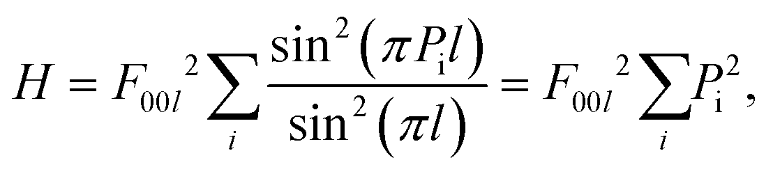 | (1) |
 | ||
| Fig. 1 (a) Two gold cuboctahedra (CUBs) merged via the (111) plane, view along [−110]. Clusters shown on the picture represent two CUBs with the original number of atoms equal to 309. The merged CUB model consists of 603 atoms (the twin plane consists of 15 atoms). (b) XRD diffraction patterns calculated for regular relaxed: gold CUB, gold CUB multiplied by 2 and two merged Au CUBs. The 111 height of the merged CUBs is 1.2 times greater than the doubled height of the regular CUB. | ||
For one CUB, there are eight equal [111] orientations; for two CUBs, the number is doubled (8 × 2). However for the merged CUBs, there are two types of [111] directions: 6 × 2 regular directions ([111]1–3 × 2) and two extended ([111]4 × 2) [111] directions. It can be expected that the resulting 111 peak height in powder diffraction is proportional to the sum of intensities over all orientations. Therefore, the 111 height of merged CUBs (HM.CUB) is higher than the height of two separated CUBs (H2.CUB):
 | (2) |
Indeed, the simulated diffraction pattern of twinned NPs reveals that the height grows about 1.2 times with respect to the doubled single NP height (Fig. 1(b)). The simulated 111 peak height enhancement is smaller than that predicted by eqn (1) because the merged CUBs share 1 common (111) plane. The extended row is only nearly doubled (minus one atom belonging to the mirror plane). Energy relaxation of the twin NP leads to a slight misalignment of the [111] rows of atoms belonging to each twin having a negligible effect on the height. From Fig. 1(b), we can notice that the considered single twinning has no effect on the 200 and 220 reflections as there is no [200] family directions (as well as [220]) that can continue across the (111) twinning planes.
Disassembling of a DEC: 111 peak heights
The DEC structure can well illustrate the combined effect of a set of twin planes: the change in peak heights and the appearance of strains. The decahedron contains five twin planes and can be divided into five equisized domains. To see only the twinning effect (without the effect of strains), we cut off the single fcc domain from the relaxed DEC, multiplied its XRD pattern by 5, and compared it with the original DEC diffraction pattern.The most noticeable difference between the diffraction patterns shown in Fig. 2(a) is the narrowing and increased height of 111, 311 and 420 peaks (the total intensity remains constant). It is noteworthy that the enhancement of the 111 peak height of a regular DEC is stronger than that in the case of two merged CUBs (Fig. 1(b)): 1.43 vs. 1.2 respectively. This difference arises from the fact that each [111] twinning contributes to the enhancement.
 | ||
| Fig. 2 (a) Comparison of the diffraction patterns of the gold DEC, one DEC domain and one DEC domain multiplied by 5. The difference marked by the orange oval is due to the twinning effect. The 111 height of the DEC is 1.43 times greater than that of a single DEC × 5. The DEC separation model consists of 4772 atoms (view along the 5-fold axis [220]) and represents equisized domains (dotted lines), avoiding the central row (17 atoms). Atoms shown in grey belong to twin planes. (b) Comparison of 111 normalized XRD patterns: stars – CUB; triangles – 1 DEC domain, crosses – domains 1 + 2, circles – domains 1 + 2 + 3, asterisks – domains 1 + 2 + 3 + 4, squares – all domains (DEC made of 4772 atoms). Details of the DEC model and its domains can be found in Table S1.† (c) XRD patterns of relaxed DEC derivatives: 1 domain (green triangles), 2 neighbour domains (yellow crosses), 3 neighbour domains (brown circles), 4 sectors (purple asterisks) and full decahedron (blue squares). The figure at the top right shows the cross-section of the volumetric strain distribution map of the relaxed DEC. | ||
The discussed diffraction pattern properties are created from the mutual orientation of the domains (not from the twin planes) and the formation of new interatomic distances. Therefore, for diffraction studies, the term “multidomain” NP is more suitable than the term “multiply-twinned” NP.
To see how the diffraction pattern changes depending on the number of domains, we disassembled the DEC into the following structures: full DEC (5 domains), 4 domain, 3 domain, 2 domain and 1 domain models. Only the original decahedron was relaxed, while its derivatives were not. This was done in order to conserve strains within the models and to track down the twinning effect alone. Since in all XRD databases the 111 peak amplitude of fcc metals equals 100, we equalized the height of 111 peaks to 100% for all the models (Fig. 2(b)).
Finally, as can be seen from Fig. 2(a) there are two groups of diffraction peaks: peaks affected and not affected by twinning. By analysing the height ratio of a not affected 200 or 220 peak to an affected 111 peak, one can determine the number of domains in the model. Fig. 2(b) demonstrates the principle of this concept: the more domains, the smaller the 220 (or 200) to 111 peak height ratio.
Disassembling of a DEC: origin of strains
It is known that there is 7.35° angle deficiency in the DEC stacking that forces atoms to move from their nodal positions.4 The disassembling approach allows us to monitor how this gap causes the appearance of expansion strains in a DEC. Fig. 2(c) shows that as the number of domains increases, after energy relaxation all the peaks move to the left-hand side, corresponding to the expansion of the lattice. One may expect that the transition from the four domain structure to the five domain structure should be accompanied by a strong expansion of the lattice, due to the necessity to fill in the 7.35° gap. However, as we can see from Fig. 2(c) this transition is characterized by moderate shifts. It means that each twinning leads to the appearance of microstrains. Fig. 1(a) shows that even a single twin plane in between two regular CUBs leads to a misalignment in the rows of atoms.Despite the expansion forces, the diffraction peaks of a single DEC domain are shifted to the right-hand side compared to those of the non-relaxed CUB (lattice constant = 4.08 Å; Fig. S2a†). In other words, comparing to the bulk value, the single DEC domain has more contracted lattice parameters. Therefore usually the expansion forces in the DEC are overridden by the contraction. This statement can be visualized with a volumetric strain analysis performed using the OVITO program, which shows only shrinking of the DEC cluster (Fig. 2(c)).28
The appearance of expansion microstrains (Fig. 2(c)) is visible only when we consequently consider relaxed 1–5 domain models. At the same time, the analysis of non-relaxed domains (with constant microstrains) allow one to monitor the strain effect, which was described by Warren.27 The stacking faults or/and 1D twin planes lead to the appearance of a new interatomic distances, causing characteristic shifts of the 111 peak to the right-hand side and the 200 peak to the left-hand side (Fig. S3a†).
Size estimation of a single domain
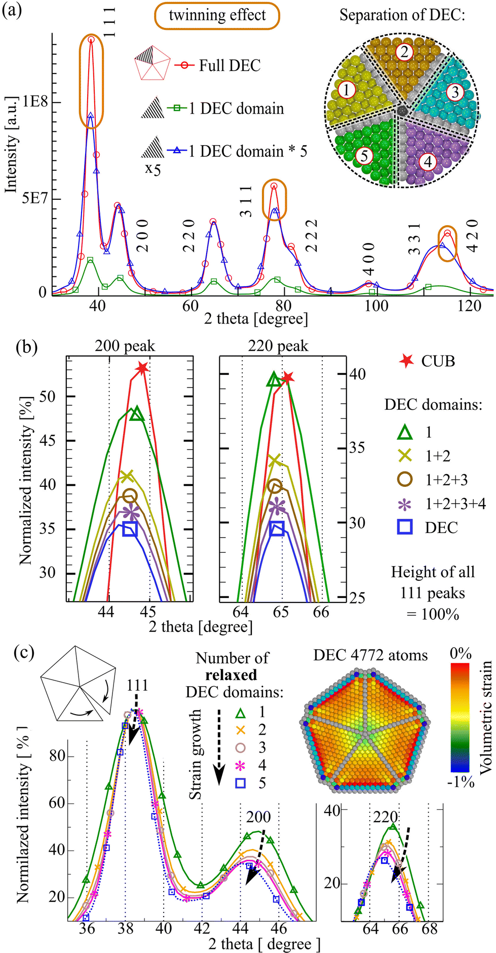
As it can be seen from Fig. 2(c) the multi-twinning also affects the peak width, and consequently, the size estimation following the Scherrer formula. Comparing the calculated XRD patterns of CUBs (2057 atoms) and DECs (4776 atoms) (Fig. 3(a)), one may notice that the full widths at half-maximum (FWHM) of the corresponding 111 peaks are similar. However, their structures and actual sizes are different. The diameter of CUB NPs calculated using the Scherrer equation from the 111 peak is ∼3.6 nm while the actual size is ∼3.8 nm. This means that the Scherrer equation works well for a single domain CUB NPs. However, for the DEC NPs it gives wrong results. The DEC NP diameter calculated from the 111 peak is 3.9 nm, and the actual size is 5.1 nm, meanwhile the diameter calculated from the 200 peak is 2.3 nm, which differs even more (Fig. S4†). | ||
Fig. 3 (a) Calculated XRD 111 and 220 peak patterns of a CUB with 2057 atoms, a DEC with 4776 atoms and 1 DEC domain with 951 atoms (separately relaxed). More details can be found in Fig. S4.† (b) H220/H111 ratio as a function of the 220 peak FWHM. 13 DEC models are separated into 1–5 domain structures. The yellow stars in the lower right corner represent two ICO models with 12![[thin space (1/6-em)]](https://www.rsc.org/images/entities/char_2009.gif) 431 and 14993 atoms (Note S2†). 431 and 14993 atoms (Note S2†). | ||
Analysis of 220 peak widths (by the Scherrer equation) of both DEC and its single domain gives the same size of−2.7 nm. This means that for DECs, the 220 peak width does not correspond to the size of the whole cluster, but rather to the size of the single domain.29 This is one of the reasons for the discrepancy between NP sizes estimated by XRD and TEM.
It should be noted that the 220 DEC peak is less sensitive to strains (Fig. 2(c)) and to the shape of the domain (Fig. S5†) than the 200 peak. We assume that it is caused by the fact that the [200] direction has a small multiplicity,8 whereas the [220] direction has 12 orientations allowing better domain size averaging. Therefore the 220 peak width can be used as an indicator of the mean size of the single domain. In addition, this peak does not overlap significantly with other peaks (there is a strong overlap only for very small NPs), which makes background line estimation easier. Taking into account all these features, we propose to use the 220 peak in further multidomain XRD analysis.
Estimation of the number of domains
As can be seen from Fig. 2(b), the ratio of heights of the 220 to 111 peaks allows one to find the number of domains in a cluster. The analytical prediction of H220/H111 seems to be possible only for models with a small number of domains. The more domains, the more difficult the prediction. Additionally, in order to apply the analytical solution to an actual sample, the Debye–Waller factor must be taken into account. However, the classical formula cannot be used, because, as follows from the simulations, the Debye–Waller factor depends on the cluster size. Therefore, in order to systematically analyse the dependence of the ratio of peak heights on the number of domains, we used extensive atomistic simulations, similar to that in Fig. 2(b).We built 13 models of Marks DEC (m = n, p = 330), with the size ranging from 3.15 to 8.95 nm. Then using molecular dynamics simulation, each model was equilibrated at 293 K for at least 30 psec, followed by separation into one, two, three and four domain structures (as it is shown in Fig. 2(b)). For each model, we calculated the diffraction pattern followed by the H220/H111 ratio analysis as a function of the FWHM of the 220 peak. The results are summarized in Fig. 3(b).
As shown in Fig. 3(b), the H220/H111 ratio decreases stepwise as the number of domains (Num. dom.) increases. The obtained dependencies can be fitted to the linear equations with a constant slope. The spacing between curves can be approximated by the natural logarithm of the number of domains (the spacing is given in the square brackets):
 | (3) |
 | (4) |
The spacing between the curves was determined in the way to minimize the difference between the obtained H220/H111 values and the fitting equation. An important aspect of the fit is the position of H220/H111 for ICO models (Fig. 3(b), yellow stars). The linear eqn (3) fits badly to ideal ICOs. This is due to the simultaneous presence of expansion and contraction elastic strains inside a single domain of an ideal ICO, which significantly enlarge the FWHM of ICO diffraction peaks.31 If we calculate the 220 FWHM ignoring the strain effect, then the eqn (3) points to the correct number of domains (Note S2†).
The dependences shown in Fig. 3(b) were obtained from the models equilibrated at 293 K. However, computational simulations often consider models at ∼0 K, after the relaxation procedure. A change in temperature affects the motion of atoms, which modifies the Debye–Waller factor. Therefore eqn (3) and (4) are not applicable to models at ∼0 K. The separate calibration for the relaxed models is shown in Fig. S5 and described in Note S3.†
Estimation of the whole cluster size
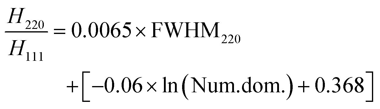
Once the size of the average single domain and the number of domains are known, it is possible to find the size of the whole cluster. This correlation can be found numerically, by analysing the size of a single domain from the 220 peak (using the Scherrer equation) and calculating the actual sizes of clusters with the CLUSTER software32 (Fig. 4(a)).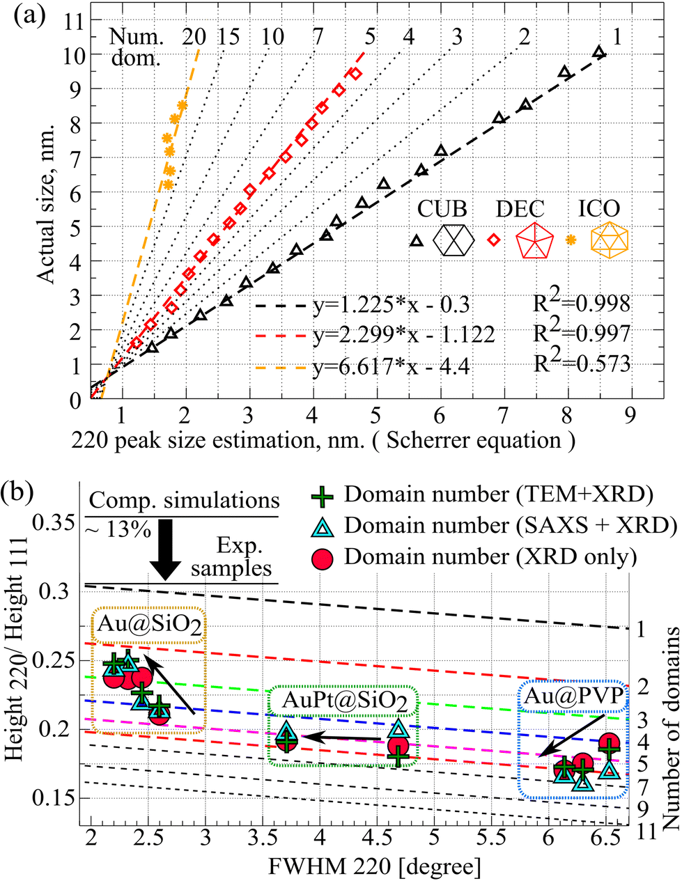 | ||
| Fig. 4 (a) Dependence of the actual cluster size on the single domain size calculated from the 220 peak (using the Scherrer equation) depending on the number of domains (Num.dom.). The black triangles represent CUB models (Table S1†); red diamonds – DEC models; yellow stars – ICO models. The dotted lines correspond to the linear fit of the simulated data (eqn (5)). (b) Domain number analysis of experimental samples by three different methods: MDXRD method alone (red circles; left y-axis); a combination of TEM grain distribution analysis (volume-weighted fraction) and XRD (shown in green pluses, right y-axis); a combination of SAXS mean size analysis (volume-weighted fraction) and XRD (shown in blue triangles, right y-axis). Black arrows show the direction of the sample transition from its initial state to the final one (after temperature/X-ray treatment). | ||
As can be seen from Fig. 4(a) there is a good linear correlation between the Scherrer size estimation and the actual size for all three morphology types. Therefore, the more domains, the greater the value of the slope. Assuming a uniform and linear change of variables, one may derive the following equation for the estimation of the whole cluster size:
| Actual size = a × Scherrer220 size + b. | (5) |
Both coefficients a and b change linearly depending on the number of domains:
| a = 0.2489 × Num.dom. + 0.9118 (R2 = 0.99) | (6) |
| b = −0.2165 × Num.dom. − 0.0639 (R2 = 0.99). | (7) |
The use of eqn (5) allows one to determine the average size of Au clusters in a sample.
Besides the perfect models divided into equal sections, the proposed method can be applied successfully to randomly multi-twinned models of nanostructures. An example is given at the end of the discussion section.
Verification of the MDXRD
To verify the introduced multidomain XRD (MDXRD) concept, we have meticulously analysed 11 samples (Table S2†). For each sample, we analysed the mean volume weighted size and the average number of domains. To assess the MDXRD accuracy, we compared its results with those obtained by reference methods: TEM and small-angle X-ray scattering (SAXS). Nine of these 11 samples (Table 1) show the direct applicability of MDXRD, the remaining two samples (Table 2) serve as examples of limitations of the method.| Group no. | Sample ID | Mean size, [nm] | ||
|---|---|---|---|---|
| MDXRD | TEM | SAXS | ||
| 1 | Au_PVP 1 | 2.2 | 2.3 | 2.6 |
| Au_PVP 2 | 2.8 | 2.7 | 3 | |
| Au_PVP 3 | 2.9 | 2.9 | 3.1 | |
| 2 | Au_PVP_SiO2 RT | 7.1 | 6.7 | 7 |
| Au_PVP_SiO2 400 °C | 5.8 | 6.3 | 6.7 | |
| Au_PVP_SiO2 500 °C | 6.9 | 6.4 | 6.5 | |
| Au_PVP_SiO2 600 °C | 6.9 | 6.7 | 6.7 | |
| 3 | Au_Pt_SiO2 RT | 3.9 | 4.2 | 3.5 |
| Au_Pt_SiO2 450 °C | 5.3 | 5.4 | 5 | |
| Group no. | Sample ID | MDXRD | TEM | SAXS | |||
|---|---|---|---|---|---|---|---|
| Dom. num. | Mean size, [nm] | Dom. num. | Mean size, [nm] | Dom. num. | Mean size, [nm] | ||
| FWHM (no correction) | |||||||
| 4 | Au@C | 6.45 | 13.89 | 0.56 | 5.79 | 2.14 | 7.97 |
| 2 | Au@PVP@SiO2 800 °C | 4.01 | 19.03 | −0.61 | 7.24 | 0.17 | 9.23 |
| Integral breadth | |||||||
| 4 | Au@C | 5.7 | 7.29 | 3.69 | 5.79 | 6.61 | 7.97 |
| 2 | Au@PVP@SiO2 800 °C | 3.7 | 10.18 | 1.58 | 7.24 | 3.01 | 9.23 |
The average number of domains can be obtained not only from XRD, but also by combining XRD with TEM and SAXS using eqn (5): the Sch.220 size values are calculated from XRD, while Act. sizes (volume weighted mean sizes) are calculated by TEM and SAXS techniques:
 | (8) |
The results obtained by combining TEM with XRD and SAXS with XRD are in good agreement. However, the number of domains obtained by MDXRD is significantly and systematically greater than values obtained by combined techniques (Fig. S6†). Since this difference is systematic, it is justified to modify the intercept part (β) of eqn (4) from 0.368 to 0.32 (eqn (9)). The origin of this shift is discussed in the section below. This correction enables achieving a good correlation between MDXRD and combined techniques (Fig. 4(b)). The obtained agreement is much better than in the case of using the regular Scherrer equation for the 111 or 220 peak or Williamson–Hall plot analysis (Table S2†).
 | (9) |
Corrections and limitations
The necessity for 13% shift of the height ratio down (from 0.368 to 0.32; Fig. 4(b)) is caused by the shape of simulated DEC domains. These domains (especially 1 domain models) are asymmetrically elongated in one direction. Therefore, the height ratio of 220 to 111 peaks is greater than that for the one domain CUB model with a more symmetrical shape, which is proved by atomistic simulations (Fig. S7†).We assume that in experimental powder diffraction, the multidomain particles consist of domains, on average, of more regular shape than that of the simulated DEC. The height ratio shift (Fig. 4(b)) is necessary to convert the theoretically calculated dependence into the experimental one. Moreover the standard X-ray powder diffraction data (e.g. JCPDS no. 04-0784) also points to the H220/H111 ratio of 0.32. This fact additionally justifies the necessity for the shift of the H220/H111 ratio.
Although Fig. 4(b) and Table 1 demonstrate a good agreement between MDXRD and other techniques, there are some applicability limitations. In principle, there are no limitations regarding the size of analysed NPs, because twinning will affect XRD patterns regardless of NP sizes. However, the multidomain method is not suitable for samples with a broad size distribution. The intensity of scattered X-rays is proportional to the volume of particles (to the number of atoms). Since the volume is proportional to the third power of the particle size, the contribution of large clusters is greater than the contribution of small ones. As a result, the XRD spectra of samples with a wide size distribution of NPs will mainly represent a large size fraction. Thereby, the mean size will be shifted towards bigger values. Also, applying combined TEM and XRD or SAXS and XRD to such samples gives meaningless results, i.e. as it can be seen from Table 2, the number of domains for the Au@C sample is varying from ∼0.6 to ∼6. The mean size analysis results also differ markedly.
Another example is the Au@PVP@SiO2 sample after treatment at 800 °C. For all previous samples (Au@PVP@SiO2 at RT, 400, 500 and 600 °C) all techniques were consistent with each other. However, at 800 °C, NPs started to grow rapidly, contributing to a high size tail in the size distribution. This results in overestimation in the mean size analysis, because X-ray diffraction is sensitive to the large size particles. The negative number of domains (for TEM + XRD) results from the size estimation of the average domain (the Scherrer equation applied to the 220 peak) that is larger than the mean size of the entire cluster (obtained by TEM), which is meaningless.
For samples with a significant broadening of the size distribution, the average single domain size can be analysed not with the FWHM but with the integral breadth of the 220 peak. This can significantly improve the consistency of the obtained results (Table 2).
To provide better statistics, analysis of six more supplementary samples (alloyed AgPt and CuAg NPs) can be found in Table S2.† These examples confirm the same trend: if the NP size distribution is narrow, the MDXRD and TEM analysis results are in agreement.
As is seen in Table 1, the multidomain approach can be directly applied only to single phase samples (monometallic and bimetallic alloy structures). The analysis of two-phase bimetallic samples is more complicated. Preliminary simulations of core–shell structures (S. Fig. 8†) showed that the multidomain approach can provide reasonable results, if the lattice constants of both metals are similar. Nevertheless, additional justification of this statement is required. Meanwhile, the structural features of Janus NPs cause a dramatic change in the profile of 220 peaks, which does not allow characterizing them by the MDXRD method.
In a broader context, the multidomain approach shows how twin planes affect XRD patterns, i.e. whenever twinning occurs, it can be noticed (as a change in a height ratio of peaks) by diffraction techniques. Since twinning is typical for hexagonal close-packed (hcp) metals, after major update, MDXRD can also be used for the analysis of these metals. However, such update requires further extensive studies, because twinning of hcp structures differs from that of fcc metals.
Apart from the features mentioned above, there are only general requirements of powder XRD that should be met: the amount and granularity of the sample must conform to a powder with the grain size lying within the system resolution and the effect of the preferred orientation should be avoided.
Additional outcomes of MDXRD
The obtained dependencies were calculated for gold. Taking into account that the platinum scattering properties are very similar to those of Au, eqn (5) and (9) can be directly applied to platinum/alloyed Au–Pt samples (Table 1). In addition, the possibility of applying MDXRD to other fcc metals can be considered. The second part of the method (eqn (5)) is not related to the material; therefore, it can be used without corrections. However, some parts of eqn (9) are material dependent. Definitely the β intercept needs to be modified as it depends on the properties of the material. The β parameter represents a height ratio of peaks H220/H111 for the bulk (FWHM ≥ 0); hence, the β value can be taken from the standard XRD database. The spacing between lines can be applied without correction as it depends on the mutual orientation of domains. The slope of the eqn (9) includes two factors: the mutual orientation of domains (independent of the fcc material) and a size dependent Debye Waller (DW) factor. The material dependent DW correction is included as a β parameter, while its size dependence is considered using molecular dynamics simulations. Therefore, to apply MDXRD to a monometallic fcc material, only one parameter is necessary – the characteristic β value. In the case of bimetallic samples, the β parameter can be found using the Vegard's law (Table S2†). Nevertheless, the further justification is required.Interestingly, Fig. 4(a) illustrates the fundamental applicability of the Scherrer equation to nanoparticles. The width of the peaks does not correspond to the entire cluster size, but rather to an averaged signal from all domains. Therefore, on applying only the Scherrer equation, the size estimation error increases with the size and the number of domains. In addition, different diffraction peaks represent the size of the “average domain” differently (Fig. S9†).
Another important aspect of the MDXRD method is the characterization of irregular multidomain structures. Such clusters may have a diffraction pattern similar to that of the regular DEC; however, their interiors are completely different. As it can be seen from Fig. 5, multidomain particles have a set of domains with random shapes and sizes. The average number of domains in such models can only be estimated using eqn (9) adapted for computational modelling (Note S3†).
 | ||
| Fig. 5 Comparison of XRD diffraction patterns of an ideal relaxed DEC and relaxed irregular Au multidomain structures consisting of approximately 5 domains (cross sections are shown). Red atoms correspond to the surface/twin plane and neighbouring defect atoms; all other colours represent ideal fcc domains. | ||
Conclusions
Although the twinning effect which leads to a change in the ratio of peak heights is known,27 the Warren's classical approach focuses on the peak shift and is a phenomenological description of the effect. The multidomain approach consistently explores these phenomena. Starting from the analysis of two merged CUBs (Fig. 1), followed by disassembly of the DEC into domains, we found how the increase of the 111 peak height depends on the number of domains (Fig. 3(b)). The second step was to find the correlation between an average single domain and the entire cluster size as a function of the number of domains (Fig. 4(a)). The combination of these two elements (eqn (3) and (5)) allowed us to perform straightforward XRD analysis of the mean particle size with accuracy, comparable to TEM and SAXS techniques (Table 1).MDXRD is based on diffraction; therefore, it is sensitive to the volume-weighted size and the large-size fraction of particles. If the grain size distribution of particles is monomodal and roughly symmetrical, the multidomain approach can be applied directly (Table 1). However, with a change in the size distribution profile and the appearance of a high size tail, the multidomain method results in significant overestimation of the mean size (Table 2). This limitation is clearly seen from experiments on heating Au@PVP@SiO2 samples (from 23 °C to 800 °C). The MDXRD analysis provided correct results at up to 600 °C, where the size distribution was not significantly extended to high sizes. At 800 °C, when the SiO2 supporting material began to evolve, initiating rapid coalescence, the multidomain approach started to overestimate the mean size. Nevertheless, although the size is overestimated, the morphology characterization remains valid, but for particles of large sizes. This limitation can be overcome to some extent by using the integral breadth (instead of the FWHM). However, in this case, the size estimate is less accurate.
The most important aspect of this work is the development of a tool for the simple morphology analysis of fcc NPs. It is shown for the first time: how the successive appearance of domains affects XRD patterns by changing the ratio of peak heights. We have demonstrated that twin planes are responsible for the formation of various strains that modify the properties of NPs. Using MDXRD, different types of morphology evolution can be followed. From Fig. 4(b) (Au@PVP series), one can see how the X-ray exposure triggers a slow growth of nanoparticles leading to an increase in the number of domains. At the same time, from the Au@SiO2 sample, ordering of the bulk morphology is observed, which can be seen as a decrease in the number of domains. In a broader context, the multidomain XRD approach is an important step towards revealing the structure–property correlations in NP studies.
Experimental
Computational simulations
To construct 3D atomistic models of fcc nanocrystals and calculate their diffraction patterns, we used the program Cluster developed by us.32,33 The program enables model construction of fcc ‘magic number’ CUBs and non-periodic ICOs and DECs.This program enables flexible model design and its energy relaxation following conjugated gradient minimization and/or molecular dynamics. The used potential scheme followed that of Sutton & Chen.34 Powder diffraction patterns were calculated via the Debye summation formula. Diffraction pattern calculation from a single oriented NP followed a simple summation of the cosine phase terms. All XRD patterns were calculated using laboratory Cu radiation.
To transform the initial decahedron into a Marks configuration (m = n, p = 3) and to divide the DEC into domains, we used the Blender software with the “Atomic Blender (PDB/XYZ)” add-on. The initial nanoparticle structure was created with the Cluster, and then imported as an XYZ file into the Blender. After manual correction the modified structures were exported as an XYZ file back to the Cluster for further computational simulations.
Irregular multidomain structures (Fig. 5) can be modelled by adding a high density of vacancies in the fcc lattice, followed by energy relaxation.
For the analysis of both simulated and experimental XRD patterns, we used the Pearson type VII function as it is the most commonly used one. All obtained dependencies (Fig. 3(b)–4(b); eqn (3)–(7)) were calculated using this function; therefore, the use of other functions may affect the results.
Sample description
For the verification of MDXRD, we prepared four main (no. 1–4) and two supplementary (no. 5–6) groups of samples:To provide better statistics for the MDXRD validation, we prepared two supplementary groups of samples. These samples were not analysed by the SAXS technique; therefore, they were considered as supplementary samples.
Experimental equipment
555.5 eV. The scattering patterns were registered with an in-vacuum detector “Eiger 9M” having CdTe sensors. All samples were mounted together with references on a sample changer under Helium gas to reduce the air scattering.
Author contributions
Ilia Smirnov conceived the project, prepared figures, synthesized NPs, performed experiments, and performed data analysis; Zbigniew Kaszkur supervised the project, contributed to refining the effect of twinning on XRD patterns, and developed and updated the Cluster program for all computational simulations; Armin Hoell edited the manuscript, performed SAXS measurements, and assisted with data analysis; Ilia Smirnov and Zbigniew Kaszkur wrote the manuscript. All authors contributed to the discussion of the results and commented on the manuscript.Conflicts of interest
There are no conflicts to declare.Acknowledgements
This work was supported by the Polish National Science Centre (NCN), grant number 2018/29/B/ST4/00710. We thank DESY for granting the beamtime for this project under proposal number: I–20210744 EC. We are grateful to Maciej Zielinski for sharing the sample and data. The authors thank Dr Sylvio Haas (Beamline Scientist in charge at beamline P62, DESY) for the technical assistance at the beamline. We thank Marion Flatken for help during the measurements at the beamline.References
- D. M. Foster, R. Ferrando and R. E. Palmer, Nat. Commun., 2018, 9, 1–6 CrossRef CAS PubMed.
- E. yakout El koraychy, C. Roncaglia, D. Nelli, M. Cerbelaud and R. Ferrando, Nanoscale Horiz., 2022, 7, 883–889 RSC.
- Y. Xia, D. Nelli, R. Ferrando, J. Yuan and Z. Y. Li, Nat. Commun., 2021, 12, 3019 CrossRef PubMed.
- C. L. Johnson, E. Snoeck, M. Ezcurdia, B. Rodríguez-González, I. Pastoriza-Santos, L. M. Liz-Marzán and M. J. Hÿtch, Nat. Mater., 2008, 7, 120–124 CrossRef CAS PubMed.
- J. Wang, G. Cao, Z. Zhang and F. Sansoz, Nanoscale, 2019, 11, 12672–12679 RSC.
- J. W. Kim, A. Ulvestad, S. Manna, R. Harder, E. E. Fullerton and O. G. Shpyrko, Nanoscale, 2017, 9, 13153–13158 RSC.
- J. Carnis, A. R. Kshirsagar, L. Wu, M. Dupraz, S. Labat, M. Texier, L. Favre, L. Gao, F. E. Oropeza, N. Gazit, E. Almog, A. Campos, J.-S. Micha, E. J. M. Hensen, S. J. Leake, T. U. Schülli, E. Rabkin, O. Thomas, R. Poloni, J. P. Hofmann and M.-I. Richard, Nat. Commun., 2021, 12, 5385 CrossRef CAS PubMed.
- M. Dupraz, N. Li, J. Carnis, L. Wu, S. Labat, C. Chatelier, R. van de Poll, J. P. Hofmann, E. Almog, S. J. Leake, Y. Watier, S. Lazarev, F. Westermeier, M. Sprung, E. J. M. Hensen, O. Thomas, E. Rabkin and M.-I. Richard, Nat. Commun., 2022, 13, 3003 CrossRef CAS PubMed.
- T. Nilsson Pingel, M. Jørgensen, A. B. Yankovich, H. Grönbeck and E. Olsson, Nat. Commun., 2018, 9, 2722 CrossRef PubMed.
- D. Kim, M. Chung, J. Carnis, S. Kim, K. Yun, J. Kang, W. Cha, M. J. Cherukara, E. Maxey, R. Harder, K. Sasikumar, S. K. R. S. Sankaranarayanan, A. Zozulya, M. Sprung, D. Riu and H. Kim, Nat. Commun., 2018, 9, 3422 CrossRef PubMed.
- C. Zhang, W. Zhang, F. Karadas, J. Low, R. Long, C. Liang, J. Wang, Z. Li and Y. Xiong, Nanoscale, 2022, 14, 7702–7710 RSC.
- M. Jørgensen and H. Grönbeck, Angew. Chem., Int. Ed., 2018, 57, 5086–5089 CrossRef PubMed.
- F. H. Kaatz, D. Y. Murzin and A. Bultheel, ACS Catal., 2021, 11, 9073–9085 CrossRef CAS.
- D. Nelli, C. Roncaglia and C. Minnai, Adv. Phys.: X, 2023, 8, 2127330 Search PubMed.
- X. Ma, H. Sun, Y. Wang, X. Wu and J. Zhang, Nano Energy, 2018, 53, 932–939 CrossRef CAS.
- X. Qian and H. S. Park, J. Mech. Phys. Solids, 2010, 58, 330–345 CrossRef CAS.
- G.-S. Park, K. S. Min, H. Kwon, S. Yoon, S. Park, J.-H. Kwon, S. Lee, J. Jo, M. Kim and S. K. Kim, Adv. Mater., 2021, 33, e2100653 CrossRef PubMed.
- L. Wang, P. Guan, J. Teng, P. Liu, D. Chen, W. Xie, D. Kong, S. Zhang, T. Zhu, Z. Zhang, E. Ma, M. Chen and X. Han, Nat. Commun., 2017, 8, 1–7 CrossRef PubMed.
- C.-C. Chen, C. Zhu, E. R. White, C.-Y. Chiu, M. C. Scott, B. C. Regan, L. D. Marks, Y. Huang and J. Miao, Nature, 2013, 496, 74–77 CrossRef CAS PubMed.
- B. H. Kim, J. Heo, S. Kim, C. F. Reboul, H. Chun, D. Kang, H. Bae, H. Hyun, J. Lim, H. Lee, B. Han, T. Hyeon, A. P. Alivisatos, P. Ercius, H. Elmlund and J. Park, Science, 2020, 368, 60–67 CrossRef CAS PubMed.
- A. F. Suzana, A. Rochet, A. R. Passos, J. P. Castro Zerba, C. C. Polo, C. V. Santilli, S. H. Pulcinelli, F. Berenguer, R. Harder, E. Maxey and F. Meneau, Nanoscale Adv., 2019, 1, 3009–3014 RSC.
- J. M. Yuk, M. Jeong, S. Y. Kim, H. K. Seo, J. Kim and J. Y. Lee, Chem. Commun., 2013, 49, 11479–11481 RSC.
- D. M. Wells, G. Rossi, R. Ferrando and R. E. Palmer, Nanoscale, 2015, 7, 6498–6503 RSC.
- A. Cervellino, C. Giannini, A. Guagliardi and D. Zanchet, Eur. Phys. J. B, 2004, 41, 485–493 CrossRef CAS.
- A. Longo and A. Martorana, J. Appl. Crystallogr., 2008, 41, 446–455 CrossRef CAS.
- L. Velterop, R. Delhez, T. H. de Keijser, E. J. Mittemeijer and D. Reefman, J. Appl. Crystallogr., 2000, 33, 296–306 CrossRef CAS.
- B. E. Warren, X-Ray Diffraction, Addison-Wesley, Reading, MA, 1969 Search PubMed.
- A. Stukowski, Modell. Simul. Mater. Sci. Eng., 2010, 18, 15012 CrossRef.
- C. Song, O. Sakata, L. S. R. Kumara, S. Kohara, A. Yang, K. Kusada, H. Kobayashi and H. Kitagawa, Sci. Rep., 2016, 6, 1–7 CrossRef PubMed.
- C. L. Cleveland, U. Landman, T. G. Schaaff, M. N. Shafigullin, P. W. Stephens and R. L. Whetten, Phys. Rev. Lett., 1997, 79, 1873–1876 CrossRef CAS.
- Z. Kaszkur and I. Smirnov, arXiv:2212.06926 [cond-mat.mtrl-sci], 2022.
- B. Mierzwa and Z. Kaszkur, in Applied Crystallography, WORLD SCIENTIFIC, 2004 Search PubMed.
- Z. Kaszkur, Program Cluster, https://www.zbigichf.ayz.pl/program-cluster/.
- A. P. Sutton and J. Chen, Philos. Mag. Lett., 1990, 61, 139–146 CrossRef.
Footnote |
| † Electronic supplementary information (ESI) available. See DOI: https://doi.org/10.1039/d3nr00456b |
| This journal is © The Royal Society of Chemistry 2023 |