
 Open Access Article
 This Open Access Article is licensed under a Creative Commons Attribution-Non Commercial 3.0 Unported Licence
Domain wall propagation and pinning induced by current pulses in cylindrical modulated nanowires†
C.
Bran
 *a,
J. A.
Fernandez-Roldan
b,
J. A.
Moreno
c,
A.
Fraile Rodríguez
de,
R. P.
del Real
a,
A.
Asenjo
a,
E.
Saugar
a,
J.
Marqués-Marchán
a,
H.
Mohammed
c,
M.
Foerster
f,
L.
Aballe
f,
J.
Kosel
cg,
M.
Vazquez
a and
O.
Chubykalo-Fesenko
a
*a,
J. A.
Fernandez-Roldan
b,
J. A.
Moreno
c,
A.
Fraile Rodríguez
de,
R. P.
del Real
a,
A.
Asenjo
a,
E.
Saugar
a,
J.
Marqués-Marchán
a,
H.
Mohammed
c,
M.
Foerster
f,
L.
Aballe
f,
J.
Kosel
cg,
M.
Vazquez
a and
O.
Chubykalo-Fesenko
a
aInstituto de Ciencia de Materiales de Madrid, CSIC, Madrid, 28049, Spain. E-mail: cristina.bran@icmm.csic.es
bHelmholtz-Zentrum Dresden-Rossendorf e.V., Institute of Ion Beam Physics and Materials Research, Bautzner Landstrasse 400, 01328 Dresden, Germany
cKing Abdullah University of Science and Technology, Computer Electrical and Mathematical Science and Engineering, Thuwal 23955-6900, Saudi Arabia
dDepartament de Física de la Matèria Condensada, Universitat de Barcelona, Barcelona, 08028, Spain
eInstitut de Nanociencia i Nanotecnologia (IN2UB), Universitat de Barcelona, Barcelona, 08028, Spain
fALBA Synchrotron Light Facility, CELLS, Barcelona, 08290, Spain
gSilicon Austria Labs, Villach 9524, Austria
First published on 10th April 2023
Abstract
The future developments in 3D magnetic nanotechnology require the control of domain wall dynamics by means of current pulses. While this has been extensively studied in 2D magnetic strips (planar nanowires), few reports on this exist in cylindrical geometry, where Bloch point domain walls are expected to have intriguing properties. Here, we report an investigation on cylindrical magnetic Ni nanowires with geometrical notches. An experimental work based on synchrotron X-ray magnetic circular dichroism (XMCD) combined with photoemission electron microscopy (PEEM) indicates that large current densities induce domain wall nucleation, while smaller currents move domain walls preferably antiparallel to the current direction. In the region where no pinning centers are present, we found a domain wall velocity of about 1 km s−1. Thermal modelling indicates that large current densities temporarily raise the temperature in the nanowire above the Curie temperature, leading to nucleation of domain walls during the system cooling. Micromagnetic modelling with a spin-torque effect shows that for intermediate current densities, Bloch point domain walls with chirality parallel to the Oersted field propagate antiparallel to the current direction. In other cases, domain walls can be bounced from the notches and/or get pinned outside their positions. We thus found that current is not only responsible for domain wall propagation, but also is a source of pinning due to the Oersted field action.
1. Introduction
Cylindrical magnetic nanowires provide versatile functionalities for data and energy storage, sensing, magnetic nanocircuits or magneto-mechanical actuators.1 They are promising candidates as building blocks for novel three-dimensional nanotechnology.2 The future implementation of such technology requires manipulation of magnetism in cylindrical magnetic nanowires by means of low power consumption stimuli such as electric currents. Spintronics is widely recognized within the scientific/technological community as a candidate for future energy-saving nano-applications.3 In comparison with the use of external fields, current-induced magnetization dynamics offers more energy efficiency. However, unlike planar nanowires, spintronics-based manipulation of magnetism in cylindrical magnetic nanowires has not yet been developed despite their great potential for high storage density and other novel multifunctionalities.Magnetic domain walls (DWs) are expected to play a decisive role as information carriers in magnetic circuits and thus manipulating their dynamics by means of electrical currents is important for future developments.4,5 Cylindrical symmetry gives rise to interesting possible magnetic configurations.6–10 Typical nanowires investigated experimentally, with diameters above 50 nm, present two types of DWs:11–13 vortex–antivortex (VAV) and the Bloch point (BP). The dynamics of both DWs is expected to be different from that of planar nanowires.14,15 For example, DWs in cylindrical geometry have been predicted to not suffer from the Walker breakdown phenomenon, characteristic of a planar geometry, and thus potentially very high velocities, above 1000 m s−1, have been theoretically predicted.15,16 Whether these velocities can be achieved experimentally is still an open question.
Although DW dynamics is well studied in planar magnetic nanowires (prepared by lithography), in cylindrical geometry only a scarce number of articles have reported experimental measurements. Ivanov et al.17 measured the motion of 3D domain walls by simultaneous application of a field and current in bi-segmented Co/Ni nanowires, estimating the DW velocity as a few hundreds of meters per second. Schöbitz et al.18 have observed current-induced domain wall motion in Ni-based nanowires by Magnetic Force Microscopy (MFM) and X-ray Magnetic Circular Dichroism (XMCD) combined with Photo-Emission Electron Microscopy (PEEM) measurements,18 estimating the velocity up to 600 m s−1. On the other hand, simulations show that during the current-induced dynamics, the BP DW may be converted into a VAV domain wall, limiting its velocity. Additionally, the Oersted field was predicted to play an important role, being the source of DW transformation and dynamics, even without the direct action of spin-transfer torques.15,16
Furthermore, if the BP DW velocities are found to be as high as theoretically predicted, the control of DW pinning will be an important aspect towards the implementation of spintronics based on cylindrical nanowires. This may be achieved by creating special notches designed to stop their propagation. While the use of notches to pin DWs is well established in planar geometry,19,20 an efficient control of DW pinning under an applied field in cylindrical nanowires has not yet been achieved.21–23
In this article, we investigate the motion of DWs in Ni cylindrical nanowires with specially designed notches. To compare their effect with straight nanowires, we fabricated them only in one part of the NW, leaving the other one free of defects. Significantly, while our experiment is successful in terms of nucleation, motion, and pinning, we also unexpectedly observed that DWs move not only in the direction antiparallel to the current (as set by the spin-transfer torque), but also in the parallel direction, i.e., against the electron flow. Our simulations (which include the spin-torque effects and the Oersted field) assist in understanding the current-induced dynamics of DWs in the presence of notches. They show that DWs can be scattered from the notches and propagate in the opposite direction. Importantly, we identified a different DW pinning mechanism when the Oersted field with the rotational sense opposite to the initial BP DW can be a source of its pinning outside the defect region.
2. Results and discussion
2.1. Experimental
Geometrically modulated cylindrical Ni nanowires with an fcc crystallographic structure were grown by electrodeposition into the pores of anodic alumina membranes (Fig. S1(b)-ESI†).24 Nanopores with a uniform diameter on one side and periodical geometrical modulations/notches on the other side were synthesized by pulsed anodization by applying a constant voltage of 130 V first for 400 s, which produces alumina pores with a constant diameter, followed by short voltage pulses of 100 and 130 V in order to produce the side of the nanopores with modulations/notches. The fabricated alumina templates were filled by electrodeposition-forming arrays of Ni nanowires. They were removed from the alumina membranes by chemical etching and deposited onto a Si substrate. Finally, they were kept in contact with Au electrodes to allow the injection of an electric current (Fig. S1(c and d)-ESI†). More details about the fabrication and contacting procedures are given in the ESI.† The SEM images of a contacted nanowire with the main diameter of about 100 nm and 13 μm length are displayed in Fig. 1(a). The nanowire shows modulations/notches at the left side (area marked in green) and a uniform cylindrical geometry (free of notches) at the right side (area marked in orange). The geometry is schematically shown in the top panel. The close-up SEM images of Fig. 1(b) and (c) correspond to the marked green and orange areas in Fig. 1(a).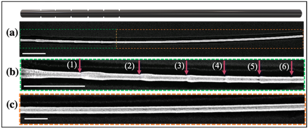 | ||
| Fig. 1 Schematic view of a contacted Ni nanowire (top panel). (a) SEM image of a contacted 13 μm Ni nanowire with notches at the left side (marked in green), (b) the close-up SEM image of the green marked area in (a), showing the position of each notch marked by red arrows, and (c) the close-up SEM image of the orange marked area in (a). The scale bar is 1 μm. | ||
As observed in Fig. 1(b), at the right side of the notches, there is some broadening in the nanowire diameter due to small variations in the current density which occurs during the anodization process.
Fig. 2 presents the XMCD-PEEM images of the same nanowire acquired at the Ni L3-edge with the X-ray incidence at about 45° to the nanowire axis, i.e., sensitive to both parallel and perpendicular magnetization components with respect to the NW axis. The top panels in Fig. 2 present the direct (XAS) image of the wire where the areas with and without notches have been marked by dashed arrows.
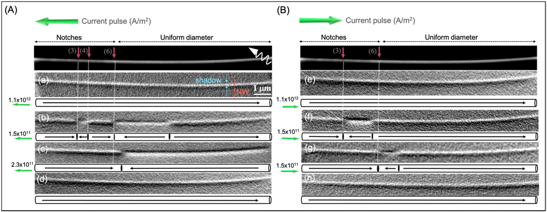 | ||
| Fig. 2 XAS images (top panel in A and B) and a sequence of the XMCD-PEEM images taken after current pulses with different intensities and polarities (indicated by the green arrows) were applied along the contacted Ni modulated nanowire. (a and e) XMCD-PEEM images of the Ni NW, presenting a single domain state. (b–d) and (f–h) XMCD-PEEM images of the Ni NW taken after current pulses of 8 ns with different amplitudes and polarities were applied along its length, as represented by the green arrows in the figure. The red arrows and the white dashed line mark the different pinning centers produced by the notches. The graphical illustrations below each PEEM image represent the magnetic configurations of the NW. | ||
Fig. 2(a) in panel (A) shows the NW in a single domain magnetic state as indicated by the uniform dark/bright XMCD contrast in the NW and its shadow,25 respectively. In the following, we refer to the contrast of the NW itself when we write “dark” or “bright” contrast.
Fig. 2(b)–(d) in panel (A) present the XMCD-PEEM images taken after current pulses of 8 ns with left polarity were applied.
In Fig. 2(b), the NW is imaged after applying a high amplitude current pulse of 1.1 × 10¹² A m−2 for 8 ns that is large enough to break the magnetization into a multidomain state, as seen from the XMCD contrast, dark/bright/dark/bright/dark. There are five magnetic domains oriented antiparallel/parallel/antiparallel/parallel/antiparallel to the polarization vector (i.e. along the NW axis with three DWs pinned at the notches labelled (3), (4) and (6) and one DW pinned in the region of the NW with a uniform diameter). The notch positions in each XMCD-PEEM image have been determined through the correlation between the direct X-ray absorption (XAS) image of the NW and the SEM data.
The orientation of the X-ray beam, around 45° away from the wire axis, provides magnetic contrast not only from the domains but also from the DWs. The bipolar contrast observed in the shadow of the DWs suggest that they are Bloch Point DWs,26 a fact confirmed also by the simulated XMCD-PEEM contrast in Fig. S3-ESI.†
After the application of a second current pulse to the magnetic state shown in Fig. 2(b) with the same polarity but a smaller amplitude, 1.5 × 10¹¹ A m−2, the state in Fig. 2(c) was obtained. The magnetic images suggest that the DW initially pinned at notch (6) has displaced towards the right, i.e., antiparallel to the current direction (along the electron flow). Note that no pinning center is present at that point.
Concerning the DWs initially pinned at notches (3) and (4), while the natural direction of motion is that the one pinned at position (3) would displace to the right, the imaging does not allow us to exclude the situation in which the DW (4) would propagate to the left, i.e. parallel to the current (opposite to the electron flow).
The overall result is that only one main domain wall is visible in Fig. 2(c). A further current pulse of 2.3 × 10¹¹ A m−2 with the same polarity, applied to the magnetic state imaged in Fig. 2(c), pushes the DW from left to the right, finally developing into a single domain state (Fig. 2(d)).
Although we have only one data set for the current density of 2.3 × 10¹¹ A m−2 where the DW has propagated outside the NW, we can estimate the lower bound of the DW velocity. Note that we have not seen additional DW nucleation at this current density. Neither did we expect a depinning of an additional DW from the right end of the NW since the pinning there is strong and even in an ideal case cannot take place without an applied field.27 Additionally, the ends of the NW are kept at 300 K and thus thermal depinning of DWs can be excluded. An estimation of the DW velocity from Fig. 2(d) for a current pulse of 2.3 × 10¹¹ A m−2, applied for 8 ns, gives rise to a value above 1000 m s−1, in agreement with the theoretical predictions15,16,28 and higher than the previously reported experimental values.17,18
Fig. 2(e) in panel B shows the NW in a single domain magnetic state as indicated by the uniform XMCD contrast. Fig. 2(f)–(h) present the XMCD-PEEM images taken after current pulses of 8 ns with right polarity were applied.
Domain walls were nucleated again by applying a high-amplitude current pulse, 1.35 × 10¹² A m−2, to the single domain magnetic state presented in (e). The resulting state, visible in Fig. 2(f), has three domains and two DWs, one pinned at notch (3) and another at the left side of notch (6). Then a sequence of low current pulses (1.5 × 10¹¹ A m−2) also with right polarity was applied to study DW propagation. In this case, both DWs seem to displace along the NW, parallel to the applied current. In Fig. 2(g), the DW at the left is pinned at notch (6) and the one at the right has stopped outside of the notch. Upon application of a new current pulse with the same intensity, the NW saturates, as can be seen from the uniform bright contrast in Fig. 2(h).
Additional information for the behavior of the DW movement is presented in Fig. S2(b) and (c).† In Fig. S2(b),† the NW is imaged before injecting a current pulse. Here, we observed three magnetic domains oriented parallel/antiparallel/parallel to the polarization vector (i.e. along the NW axis). By injecting an intermediate current pulse of 5 × 10¹¹ A m−2, the DWs, one pinned at the notch (6) and the other, outside of the notch (right-side end of the NW), move along the current, parallel to it, and the NW gets saturated, as can be observed from the uniform dark contrast in Fig. S2(c).† Note that at these intermediate current densities, thermal depinning can be expected (see below).
To summarize the effect of the current, we observed that (i) large current densities (1012 A m−2) produce DW nucleation, wherein the DW appeared to be pinned after the pulse was switched off (Fig. 2(b) and (f)). (ii) Smaller currents (1011 A m−2) move DWs. The results show DW dynamics with a lower current density compared to that predicted in cylindrical nanowires with a smaller diameter for transverse domain walls.15 We attribute this fact to the higher Bloch point domain wall mobility as compared to the transverse one.16,18 While the largest DW propagation occurs antiparallel to the current direction (i.e. along the electron flow as is expected and previously reported17), some propagation parallel to the current is also observed. (iii) Some domain walls are stopped at notches (particularly notch (6)). However, others are stopped at different inter-notch places and their positions are not reproducible. This suggests a different pinning mechanism which cannot be fully ascribed to microstructural defects and modulations. Note that DW propagation in the direction of the applied current as well as the pinning after the application of low-amplitude current pulses take place in the left part of the NW, i.e. where the notches are present, while in the right part, without notches, the propagation is smooth and always against the current. (iv) For intermediate current pulses, the domain walls move both parallel and antiparallel to the current direction. This happens also in the right part of the NW presented in Fig. S2(c)† (for much higher current densities), which we attribute to thermal domain wall depinning. All of the above indicates an important role of the notches in current-induced domain wall dynamics.
2.2. Micromagnetic modelling
To understand the experimental behavior, we first assessed the temperature rise due to the Joule heating by the current pulse of realistic temporal shape and a maximum current density at 8 ns (more details in the Methods section and the ESI†). The simulations show that temperature reaches the maximum value at the timescale of 9 ns and decays to the ambient temperature in the ca. 40–50 ns timescale. Fig. 3(a) presents the calculated maximum temperature distribution during the application of current along the direction of the axis in a single Ni NW, showing that its maximum is reached at about 300 nm from the NW ends. Note that in the simulations the temperature at the ends is maintained at 300 K due to the presence of contacts. Our modelling shows that the current pulses with magnitudes higher than 8 × 10¹¹ A m−2 raise the temperature in the middle of the NW above the Curie temperature (for Ni, Tc = 628 K (ref. 29)). For a current pulse of 3 × 10¹¹ A m−2, the temperature increase is around 30 K, while for 1 × 10¹¹ A m−2, it is only a few K.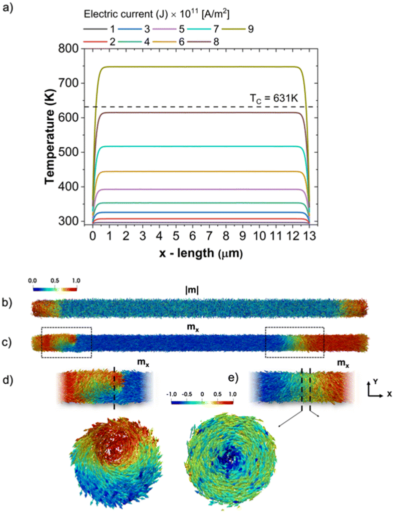 | ||
| Fig. 3 (a) The simulated temperature profile along the nanowire for different values of the current densities. (b and c) Results of thermal micromagnetic modelling showing the magnetization distribution in the wire during (b) and after the current pulse (c) for a temperature profile of 650 K. The images (d) and (e) show nucleated DWs of VAV (d) and BP type (e). The cross-sectional images of each domain wall are presented in the bottom panel. | ||
To model thermal nucleation with high current densities, we used a micromagnetic framework based on the Landau–Lifshitz–Bloch equation30 with thermal fluctuations31 (more details in the Method section and the ESI†). Importantly, these micromagnetics is a valid approach close and above the Curie temperature, Tc. The assumed temperature profile follows the one obtained using COMSOL Multiphysics® software at 9 ns and lasts 50 ns. Our simulations show that the current pulses with magnitudes corresponding to the heating below Tc do not lead to any DW nucleation, neither during the heat pulse nor after it, speaking in favor of a large energy barrier for this process. Fig. 3(b) shows the modulus of the reduced magnetization during the pulse when the maximum temperature of 650 K (higher than Tc) was reached. The wire presents nearly null magnetization at its center while still being ferromagnetic at the edges due to the cooling effects of the electrodes.
Fig. 3(c) shows the results of nucleation after a temperature profile with a maximum temperature of 650 K being applied. Importantly, nucleation occurs after the temperature pulse, i.e. during cooling down of the magnetic system. The results show a pair of nucleated DWs: one was of the VAV type (left in Fig. 3(c) and the augmented image in Fig. 3(d)), and another – of the BP type (right in Fig. 3(c) and the augmented image in Fig. 3(e)). In the simulated system, these DWs propagate in the opposite directions in the absence of any external stimuli. In a realistic situation, they may be pinned at some pinning centers such as magnetic notches and defects. Note that the type of nucleated DW is arbitrary and will vary in simulations with different temperature disorders.
We turn now to the computational results of magnetization dynamics at low current densities, considering the temperature fluctuations being less relevant (more details in the ESI†). The geometry represents a cylindrical NW of 100 nm in diameter and several microns in length with three notches and a pre-nucleated BP DW (initially pinned at the central notch for convenience). Based on the experimental data presented here and also previous reports indicating that the VAV DW is transformed to a BP DW during the dynamics,26,32 we considered only the last case. The current interacts with magnetization through the Zhang-Li spin transfer torque and the associated Oersted field33 (more details in the ESI†). Note that two types of BP domain walls can exist: one with a rotational sense parallel to the Oersted field direction (called here as “good” chirality) and the other one – with a rotational sense antiparallel to it (“bad” chirality BP DW). The BP DW is followed by the intersection of three iso-surfaces defined by mx = 0 (parallel to NW and coloured in red), my = 0 (coloured in green), and mz = 0 (coloured in blue).
Our modelling results of DW dynamics with the current switched on are presented in Fig. 4 and 5. It is worth to mention that the XMCD-PEEM images were collected in a stationary situation after the current was switched off and DWs were stopped, while the simulations allowed us to understand the dynamic processes during the current application. The simulations show that in all cases the DW dynamics is finished at 8 ns (either because a fast DW propagated outside the NW or it stopped the propagation due to pinning), thus the pictures at 8 ns will reflect the stationary situation.
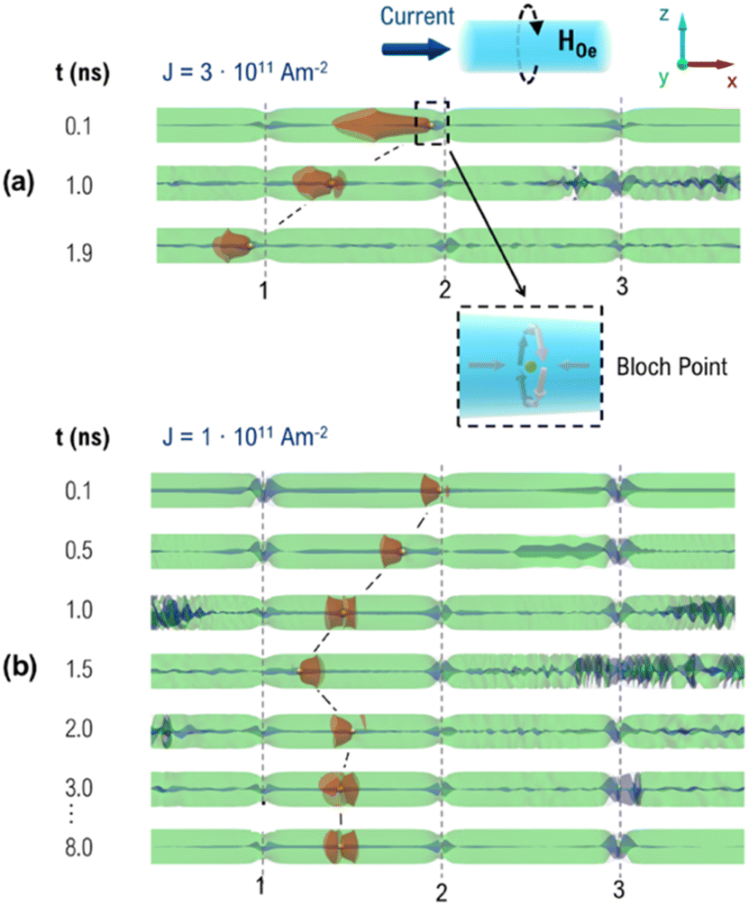 | ||
| Fig. 4 Dynamics of a Bloch point domain wall with ‘good’ chirality under two applied current densities in a nanowire with three geometrical notches labelled 1–3. The dark blue arrow above the images indicates the current direction, while the dashed black arrow – the direction of the Oersted field (HOe). The BP DW characteristics (close-up image) are presented in the inset (dashed square), i.e., initially, the DW has a head-to-head structure with a counter-clockwise rotational sense coinciding with that of the Oersted field. The iso-surfaces of the x-, y-and z-zero components of magnetization are coloured in red, green and blue and the yellow sphere indicates the position of the Bloch point. (a) The Bloch point with ‘good’ chirality propagates in the direction opposite to the driving spin-polarized current for an intermediate current density J = 3 × 10¹¹ A m−1. (b) A low current density J = 1 × 10¹¹ A m−1 results in domain wall recoil from the pinning center and temporal propagation in the opposite direction. | ||
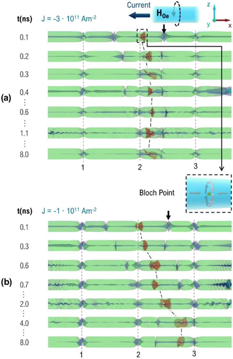 | ||
| Fig. 5 Dynamics of the Bloch point (marked by the black arrows) with ‘bad’ chirality under two applied current densities in a nanowire with three geometrical constrictions. The dark blue arrow above the images indicates the current direction, while the dashed black arrow – the direction of the Oersted field. The BP DW characteristics (close-up image) are presented in the inset (dashed square), i.e., initially, the DW has a head-to-head structure with a counter-clockwise rotational sense opposite to that of the Oersted field. Red, green and blue colours represent the isosurfaces of mx = 0, my = 0 and mz = 0, respectively. (a) The Bloch point with ‘bad’ chirality is pinned by the effect of the Oersted field produced by a spin-polarized current for an intermediate current density J = −3 × 10¹¹ A m−1. The black arrows indicate quasi-domain walls created by the encounter of two chirality domains: from the BP DW and that created by the Oersted field. (b) At a low current density J = −1 × 10¹¹ A m−1, the domain wall propagates in the direction opposite to the driving spin-polarized current until it is bounced from the notch. | ||
The modelling results indicate that under the considered current densities (1 × 10¹¹–4 × 10¹¹ A m−2), the DW always gets unpinned from the central notch. The large-distance propagation typically occurs in the NW axis following the direction antiparallel to the current (indicated by dark blue arrows on the top of the graphs), i.e. in the direction of the electron flow. This result is general for negative (left) and positive (right) applied currents and explains the main direction of the propagation in the experimental results. It also corresponds to the sign of a non-adiabatic spin-transfer torque reflecting the direction of the electron flow. Note the complex dynamic DW structure (indicated by the iso-surface with mx = 0, the reddish region), which is dynamically changing during the propagation (called the “butterfly” DW). An important remark is that only a BP DW with “good” chirality driven by intermediate current densities can cross the whole NW without pinning, see Fig. 4(a). For all other situations, we observe a pinning process either near the left notch (small current densities and “good” BP chirality, Fig. 4(b)) or near to the right notch (small current densities and “bad” BP chirality, Fig. 5(b)) or even in the middle constriction (large current densities and “bad” BP chirality, Fig. 5(a)).
An inspection of the pinning process for low positive currents (“good” DW chirality) in Fig. 4(b) indicates that the BP is first unpinned from the middle notch but then recoils (bounces) when approaching the neighbouring notch, which leads to its propagation in the opposite direction, and finally it stops at an intermediate position in the segment after few nanoseconds. We attribute this recoil to the presence of small chiral structures (not spatially resolvable by PEEM) created at the notches. Due to magnetostatic energy minimization, together with the action of a different local Oersted field, the magnetization at the notch acquires certain circulations (visible as blueish regions in Fig. 4 and 5). These structures interact with the DW and are responsible for its repulsion from the notch. Also, note a strong emission of spin-waves from NW ends and notches, which can also interact with the DW.
The same DW is of the “bad” chirality type when the current is applied in the opposite direction. These DWs may experience a chirality switching;26,32 however, we did not observe it in these particular cases (see the results in Fig. 5). For negative currents (oriented to the left), DW first propagates to the right and is pinned close to the right notch. What is striking is that for higher currents this DW gets stopped near the initial pinning site but at a position farther from the notch. This effect is due to the Oersted field creating an azimuthal magnetization component with the direction opposite to that of the BP DW, and thus there appears one more quasi-domain wall (indicated by black arrows), where two chirality domains meet each other. This quasi-domain wall, which is induced by the Oersted field, is quite robust and topologically protected (since in order to annihilate it, one would need to unwind one of the chirality) and is a source of pinning for the initial Bloch point wall. A similar quasi-domain wall is created at the left side from the original domain wall. Both, together produce its pinning.
In summary, the simulations show that BP DW with “good” chirality move under current, but can be reflected from notches, moving more efficiently at a higher current density. In contrast, the results are different for the “bad” chirality BP DW: while at low current densities, an equivalent motion as for the “good” chirality is observed, at higher current densities, a pinning by the Oersted field sets in, cancelling any motion under these conditions. Thus, DW mobility is limited by the “bad” chirality only at a high current density, but is not affected at a low current density.
3. Conclusions
In conclusion, by combined theoretical and experimental studies we have demonstrated the possibility to move Bloch point domain walls by means of current pulses in modulated Ni nanowires. First, domain walls were nucleated by current pulses with a high amplitude, which raised the temperature in the middle part of the nanowire above the Curie temperature and provided thermally induced stochastic nucleation. When the system cools down, these domain walls appeared pinned at the notches. For smaller currents, domain walls can be moved. As expected, the largest domain wall propagation occurs in the direction antiparallel to the applied current direction (parallel to the electron flow) and the pinning occurs at the notches. Unexpectedly, we also observed short-distance propagation in the direction parallel to the current as well as pinning of domain walls outside the notches. Our dynamical simulations help in ascertaining the origin of these effects. We have identified two different pinning mechanisms for domain walls in cylindrical nanowires: one related to the effect of notches themselves and another induced by the Oersted field which creates quasi-domain walls of chiral nature. As for the first mechanism, it seems that the pinning is additionally assisted by the Oersted field and a more efficient control can be expected than that with an external field. For the latter case, to our knowledge, this is the first time that this mechanism is reported. Importantly, it is not related to the presence of notches and will limit the “bad chirality” domain wall propagation in spintronic devices. Finally, we cannot exclude the influence of thermal depinning mechanisms for intermediate current densities.An important finding is our estimation of the domain wall velocity in the region free of pinning centres, as high as theoretically predicted, i.e., of the order of 1 km s−1, and higher than previously observed experimentally. We also report lower current densities which move DWs as compared to the previously reported results. We believe our results to be of high significance for further development of spintronic applications based on cylindrical magnetic nanowires.
4. Methods
4.1. Synthesis and preparation
Ni nanowires with imprinted notches along their length were produced in anodic aluminum oxide (AAO) templates.24,34–36 The modulated pores of the AAO templates were fabricated by pulsed hard anodization (Fig. S1(a)†) in oxalic aqueous solution. The nanowires were deposited in the fabricated pores by electrodeposition in a three-electrode cell using a single Watts-type bath containing 0.38 M NiSO4·7H2O, 0.08 M NiCl2·6H2O and 0.16 M H3BO3 at a constant voltage of 1 V for about 40 minutes.The total length of the nanowires in the membrane is about 28 μm. The center-to-center inter-pore distance is kept constant at 320 nm (see Fig. S1(b)†).
After the alumina template was dissolved by chemical etching, the nanowires were dispersed on a Si/SiO2 substrate and electrically contacted. More details about the sample preparation are presented in the ESI file.†
4.2. XMCD-PEEM measurements
The XMCD-PEEM measurements were performed at the CIRCE beamline of the ALBA Synchrotron Light Facility (Barcelona, Spain) using an ELMITEC LEEM III instrument with an energy analyzer.37 The samples were illuminated with circularly polarized X-rays at a grazing angle of 16° with respect to the surface. The emitted photoelectrons (low energy secondary electron with ca. 1 eV kinetic energy) used to form the surface image are proportional to the X-ray absorption coefficient and thus the element-specific magnetic domain configuration is given by the pixel-wise asymmetry of two PEEM images sequentially recorded with left-and right-handed circularly polarized light.37,38 Sample holders with integrated printed circuit board (PCB)39 were used for the injection of current pulses into the NW, with ultrasonic wire bonds as connections to the gold electrode of the sample.4.3. Micromagnetic modelling
The thermal simulations of individual modulated Ni nanowires have been carried out using COMSOL Multiphysics® software to determine the temperature in the system under the influence of the current pulses with a rise time of 8 ns and total duration of 15 ns. We assume a 13 μm Ni nanowire slightly buried in the SiO2 substrate and Cr/Au contacts maintained at 300 K. More details are present in the ESI.†Micromagnetic simulations: Thermal nucleation close to and above the Curie temperature with spatial temperature profiles calculated from COMSOL Multiphysics® simulations has been investigated using a home-made micromagnetic code based on the Landau–Lifshitz–Bloch approach. A current pulse duration up to 50 ns was considered to emulate the heat accumulation in the system. The simulations of non-thermal magnetization dynamics were done using Landau–Lifshitz–Gilbert micromagnetics with a Zhang-Li spin-transfer torque as implemented in the Mumax program.40 DW dynamics was investigated under a spin-polarized current with polarization (P = 0.5), non-adiabaticity (ξ = 0.1) and damping (0.02) in a Ni nanowire with the standard parameters of Ni used in previous studies41 (more details in the ESI†). Importantly, here the Oersted field takes into account the reduced current density in the modulations.
Conflicts of interest
There are no conflicts to declare.Acknowledgements
This work was supported by the grants PID2019-108075RB-C31 funded by the Ministry of Science and Innovation MCIN/AEI/10.13039/501100011033 and S2018/NMT-4321 NANOMAGCOST-CM funded by the Government of Madrid Region, Spain. We acknowledge the service from the MiNa Laboratory at IMN and the funding from CM (project SpaceTec, S2013/ICE2822), MINECO (project CSIC13-4E-1794), and EU (FEDER, FSE).References
- Magnetic Nano- and Microwires: Design, Synthesis, Properties and Applications, ed. M. Vazquez, Woodhead Publishing, Elsevier, 2nd edn, 2020 Search PubMed.
- A. Fernández-Pacheco, R. Streubel, O. Fruchart, R. Hertel, P. Fischer and R. P. Cowburn, Nat. Commun., 2017, 8, 15756 CrossRef PubMed.
- E. Y. Vedmedenko, R. K. Kawakami, D. D. Sheka, P. Gambardella, A. Kirilyuk, A. Hirohata, C. Binek, O. Chubykalo-Fesenko, S. Sanvito, B. J. Kirby, J. Grollier, K. Everschor-Sitte, T. Kampfrath, C.-Y. You and A. Berger, J. Phys. D: Appl. Phys., 2020, 53(45), 453001 CrossRef CAS.
- D. Atkinson, D. A. Allwood, G. Xiong, M. D. Cooke, C. C. Faulkner and R. P. Cowburn, Nat. Mater., 2003, 2(2), 85–87 CrossRef CAS PubMed.
- R. Hertel, J. Phys. Condens. Matter, 2016, 28(48), 483002 CrossRef CAS PubMed.
- I. M. Andersen, L. A. Rodríguez, C. Bran, C. Marcelot, S. Joulie, T. Hungria, M. Vazquez, C. Gatel and E. Snoeck, ACS Nano, 2020, 1399–1405 CrossRef CAS PubMed.
- C. Bran, J. A. Fernandez-Roldan, E. M. Palmero, E. Berganza, J. Guzman, R. P. Del Real, A. Asenjo, A. Fraile Rodríguez, M. Foerster, L. Aballe, O. Chubykalo-Fesenko and M. Vazquez, Phys. Rev. B: Condens. Matter Mater. Phys., 2017, 96(12), 125415 CrossRef.
- L. A. Rodríguez, C. Bran, D. Reyes, E. Berganza, M. Vázquez, C. Gatel, E. Snoeck and A. Asenjo, ACS Nano, 2016, 10(10), 9669–9678 CrossRef PubMed.
- S. Allende, D. Altbir and K. Nielsch, Phys. Rev. B: Condens. Matter Mater. Phys., 2009, 80(17), 174402 CrossRef.
- C. Bran, J. A. Fernandez-Roldan, R. P. Del Real, A. Asenjo, Y.-S. Chen, J. Zhang, X. Zhang, A. Fraile Rodríguez, M. Foerster, L. Aballe, O. Chubykalo-Fesenko and M. Vazquez, ACS Nano, 2020, 14(10), 12819–12827 CrossRef CAS PubMed.
- C. A. Ferguson, D. A. Maclaren and S. McVitie, J. Magn. Magn. Mater., 2015, 381, 457–462 CrossRef CAS.
- S. Jamet, N. Rougemaille, J. C. Toussaint and O. Fruchart, Magnetic Nano- and Microwires, ed. M. Vázquez, in Woodhead Publishing Series in Electronic and Optical Materials, Woodhead Publishing, 2015, pp. 783–811 Search PubMed.
- R. Moreno, V. L. Carvalho-Santos, D. Altbir and O. Chubykalo-Fesenko, J. Magn. Magn. Mater., 2022, 542, 168495 CrossRef CAS.
- R. Wieser, E. Y. Vedmedenko, P. Weinberger and R. Wiesendanger, Phys. Rev. B: Condens. Matter Mater. Phys., 2010, 82(14), 144430 CrossRef.
- M. Yan, A. Kákay, S. Gliga and R. Hertel, Phys. Rev. Lett., 2010, 104(5), 57201 CrossRef PubMed.
- X.-P. Ma, J. Zheng, H.-G. Piao, D.-H. Kim and P. Fischer, Appl. Phys. Lett., 2020, 117, 062402 CrossRef.
- Y. P. Ivanov, A. Chuvilin, S. Lopatin and J. Kosel, ACS Nano, 2016, 10(5), 5326–5332 CrossRef CAS PubMed.
- M. Schöbitz, A. De Riz, S. Martin, S. Bochmann, C. Thirion, J. Vogel, M. Foerster, L. Aballe, T. O. Menteş, A. Locatelli, F. Genuzio, S. Le-Denmat, L. Cagnon, J. C. Toussaint, D. Gusakova, J. Bachmann and O. Fruchart, Phys. Rev. Lett., 2019, 123(21), 217201 CrossRef PubMed.
- S. S. P. Parkin, M. Hayashi and L. Thomas, Science, 2008, 320(5873), 190–194 CrossRef CAS PubMed.
- H. Y. Yuan and X. R. Wang, Phys. Rev. B: Condens. Matter Mater. Phys., 2015, 92, 054419 CrossRef.
- E. M. Palmero, M. Méndez, S. González, C. Bran, V. Vega, M. Vázquez and V. M. Prida, Nano Res., 2019, 12(7), 1547–1553 CrossRef CAS.
- C. Bran, E. Berganza, J. A. Fernandez-Roldan, E. M. Palmero, J. Meier, E. Calle, M. Jaafar, M. Foerster, L. Aballe, A. Fraile Rodríguez, O. Chubykalo-Fesenko and M. Vazquez, ACS Nano, 2018, 12(6), 5932–5939 CrossRef CAS PubMed.
- S. Ruiz-Gómez, M. Foerster, L. Aballe, M. P. Proenca, I. Lucas, J. L. Prieto, A. Mascaraque, J. de la Figuera, A. Quesada and L. Pérez, Sci. Rep., 2018, 8(1), 16695 CrossRef PubMed.
- C. Bran, J. A. Fernandez-Roldan, R. P. del Real, A. Asenjo, O. Chubykalo-Fesenko and M. Vazquez, Nanomaterials, 2021, 11(3), 600 CrossRef CAS PubMed.
- C. Bran, E. Berganza, E. M. Palmero, J. A. Fernandez-Roldan, R. P. Del Real, L. Aballe, M. Foerster, A. Asenjo, A. Fraile Rodríguez and M. Vazquez, J. Mater. Chem. C, 2016, 4(5), 978–984 RSC.
- A. Wartelle, B. Trapp, M. Staňo, C. Thirion, S. Bochmann, J. Bachmann, M. Foerster, L. Aballe, T. O. Menteş, A. Locatelli, A. Sala, L. Cagnon, J.-C. Toussaint and O. Fruchart, Phys. Rev. B, 2019, 99(2), 24433 CrossRef CAS.
- J. A. Fernandez-Roldan, R. P. del Real, C. Bran, M. Vazquez and O. Chubykalo-Fesenko, Phys. Rev. B, 2020, 102(2), 024421 CrossRef CAS.
- H.-G. Piao, J.-H. Shim, D. Djuhana and D.-H. Kim, Appl. Phys. Lett., 2013, 102(11), 112405 CrossRef.
- C. Kittel, Introduction to Solid State Physics, 8th edn, 2004 Search PubMed.
- N. Kazantseva, D. Hinzke, U. Nowak, R. W. Chantrell, U. Atxitia and O. Chubykalo-Fesenko, Phys. Rev. B: Condens. Matter Mater. Phys., 2008, 77(18), 184428 CrossRef.
- R. F. L. Evans, D. Hinzke, U. Atxitia, U. Nowak, R. W. Chantrell and O. Chubykalo-Fesenko, Phys. Rev. B: Condens. Matter Mater. Phys., 2012, 85(1), 014433 CrossRef.
- A. De Riz, J. Hurst, M. Schöbitz, C. Thirion, J. Bachmann, J. C. Toussaint, O. Fruchart and D. Gusakova, Phys. Rev. B, 2021, 103(5), 054430 CAS.
- J. A. Fernandez-Roldan, R. P. Del Real, C. Bran, M. Vazquez and O. Chubykalo-Fesenko, Phys. Rev. B, 2020, 102(2), 1–6 CrossRef.
- W. Lee and S.-J. Park, Chem. Rev., 2014, 114, 7487 CrossRef CAS PubMed.
- M. S. Salem, P. Sergelius, R. M. Corona, J. Escrig, D. Görlitz and K. Nielsch, Nanoscale, 2013, 5(9), 3941 RSC.
- K. Pitzschel, J. M. Moreno, J. Escrig, O. Albrecht, K. Nielsch and J. Bachmann, ACS Nano, 2009, 3(11), 3463–3468 CrossRef CAS PubMed.
- L. Aballe, M. Foerster, E. Pellegrin, J. Nicolas and S. Ferrer, J. Synchrotron Radiat., 2015, 22(3), 745–752 CAS.
- J. Kimling, F. Kronast, S. Martens, T. Böhnert, M. Martens, J. Herrero-Albillos, L. Tati-Bismaths, U. Merkt, K. Nielsch and G. Meier, Phys. Rev. B: Condens. Matter Mater. Phys., 2011, 84(17), 174406 CrossRef.
- M. Foerster, J. Prat, V. Massana, N. Gonzalez, A. Fontsere, B. Molas, O. Matilla, E. Pellegrin and L. Aballe, Ultramicroscopy, 2016, 171, 63–69 CAS.
- A. Vansteenkiste, J. Leliaert, M. Dvornik, M. Helsen, F. Garcia-Sanchez and B. Van Waeyenberge, AIP Adv., 2014, 4(10), 107133 CrossRef.
- Y. Liu, D. J. Sellmyer and D. Shindo, Handbook of Advanced Magnetic Materials: Nanostructural Effects, Springer Berlin Heidelberg, Berlin, 2005 Search PubMed.
Footnote |
| † Electronic supplementary information (ESI) available. See DOI: https://doi.org/10.1039/d3nr00455d |
| This journal is © The Royal Society of Chemistry 2023 |