
 Open Access Article
 This Open Access Article is licensed under a
 Creative Commons Attribution 3.0 Unported Licence
Photon bunching in cathodoluminescence induced by indirect electron excitation†‡
Vasudevan
Iyer
a,
Kevin
Roccapriore
a,
Jacob
Ng
b,
Bernadeta
Srijanto
a,
David
Lingerfelt
 a and
Benjamin
Lawrie
*ac
a and
Benjamin
Lawrie
*ac
aCenter for Nanophase Materials Sciences, Oak Ridge National Laboratory, Oak Ridge, TN 37831, USA. E-mail: lawriebj@ornl.gov
bTechnical University of Denmark, 2800 Kongens Lyngby, Denmark
cMaterials Science and Technology Division, Oak Ridge National Laboratory, Oak Ridge, TN 37831, USA
First published on 16th May 2023
Abstract
The impulsive excitation of ensembles of excitons or color centers by a high-energy electron beam results in the observation of photon bunching in the second-order correlation function of the cathodoluminescence generated by those emitters. Photon bunching in cathodoluminescence microscopy can be used to resolve the excited-state dynamics and the excitation and emission efficiency of nanoscale materials, and it can be used to probe interactions between emitters and nanophotonic cavities. Unfortunately, the required integration times for these measurements can be problematic for beam-sensitive materials. Here, we report substantial changes in the measured bunching induced by indirect electron interactions (with indirect electron excitation inducing g2(0) values approaching 104). This result is critical to the interpretation of g2(τ) in cathodoluminescence microscopies, and, more importantly, it provides a foundation for the nanoscale characterization of optical properties in beam-sensitive materials.
1 Introduction
Cathodoluminescence (CL) microscopies have become workhorse tools for the characterization of nanomaterials with spatial resolution well beyond the optical diffraction limit.1–6 As a result of near-field, high-energy, electron interactions, CL provides access to excitation pathways not accessible in conventional optical microscopies.7 Furthermore, time-resolved CL has emerged as a crucial tool for probing ultrafast dynamics of excited states in nanoscale materials.8,9 Time-resolved CL can rely on pulsed electron beams generated with electrostatic beam-blankers10 or pulsed-laser excitation of the electron gun,11 but both of these approaches reduce the spatial resolution of the microscope and add to the complexity of the microscope column design. Ultrafast beam blankers in scanning electron microscopes (SEMs) limit the temporal resolution to ∼100 picoseconds and provide spatial resolution of ∼50 nm.12 Pulsed laser excitation of the emitter leads to sub-ps electron pulses at the expense of poor spatial resolution.13,14Measures of the CL second order correlation function g2(τ) in electron microscopes with continuous wave electron beams can provide access to nanoscale dynamics without recourse to pulsed electron sources.15–18 Moreover, spatially resolved measurements of g2(τ) can be used to extract the excitation and emission efficiency with few-nanometer resolution.19
CL bunching is typically understood as a result of high energy electron excitation of bulk plasmons, each of which can excite multiple defect centers within a sub-picosecond window.9 In diamond, for example, high energy electrons can efficiently excite a 30 eV bulk plasmon mode.20 However, the indirect excitation mechanisms involved in the generation of bunched photons have not been investigated in detail so far. While bulk-plasmon mediated CL bunching has been explored carefully, CL bunching for electron-beams incident on a substrate at some distance from color centers or excitons of interest has not been explored carefully. Similarly, the effect of aloof excitations and secondary electron excitations on CL bunching has not been described until now.
In this article, we study the effect of bulk plasmons and secondary and aloof electron excitations on the measured CL bunching for nitrogen vacancy (NV) centers in nanodiamonds using g2(τ) CL mapping supported by Monte-Carlo simulations and analytical modeling. We show that indirect excitation pathways can substantially modify the measured photon bunching, and we observe an exponential increase in g2(0) as the electron beam moves away from the nanodiamond, reaching values approaching g2(0) ∼ 10![[thin space (1/6-em)]](https://www.rsc.org/images/entities/char_2009.gif) 000, hundreds of times greater than the g2(0) measured for the same electron beam directly incident on the nanodiamond. We study the role of the substrate on the measured photon bunching and compare g2(τ) for nanodiamonds deposited on metallic (aluminum) and insulating (SiO2) films. We also probe aloof excitation pathways directly with nanodiamonds suspended over holes in a SiN membrane.
000, hundreds of times greater than the g2(0) measured for the same electron beam directly incident on the nanodiamond. We study the role of the substrate on the measured photon bunching and compare g2(τ) for nanodiamonds deposited on metallic (aluminum) and insulating (SiO2) films. We also probe aloof excitation pathways directly with nanodiamonds suspended over holes in a SiN membrane.
2 Experimental methods
Fluorescent nanodiamonds (Adamas Nano) with an average particle size of 140 nm were dropcast on a SiN membrane and on a patterned sample comprising 50 nm thick aluminum pads on a continuous 300 nm thick SiO2 film on a silicon substrate (which allowed for direct comparison of the NV CL photon statistics on Al and on SiO2 under identical imaging conditions). Each nanoparticle contains ∼1200 NV0 centers; this defect density is high enough to suppress any spatial heterogeneity in the CL emitted from the nanodiamond, consistent with other reports in the literature.21CL microscopy was performed in a FEI Quattro SEM with a Delmic Sparc CL collection system. The electron beam excites the sample through a hole in a parabolic mirror. The mirror collimates the CL emission, which is sent to an Andor Kymera spectrometer for spectrum mapping or to a Hanbury Brown–Twiss interferometer for g2(τ) measurements. The Hanbury Brown–Twiss interferometer comprises a fiber beamsplitter and a pair of Quantum Opus large area superconducting nanowire single photon detectors (SNSPDs), as shown in Fig. 1(a). Detected photons are time tagged by a HydraHarp 400 time-interval analyzer with 128 ps bin sizes. The secondary electron (SE) signal is simultaneously measured on an Everhart–Thornley detector.
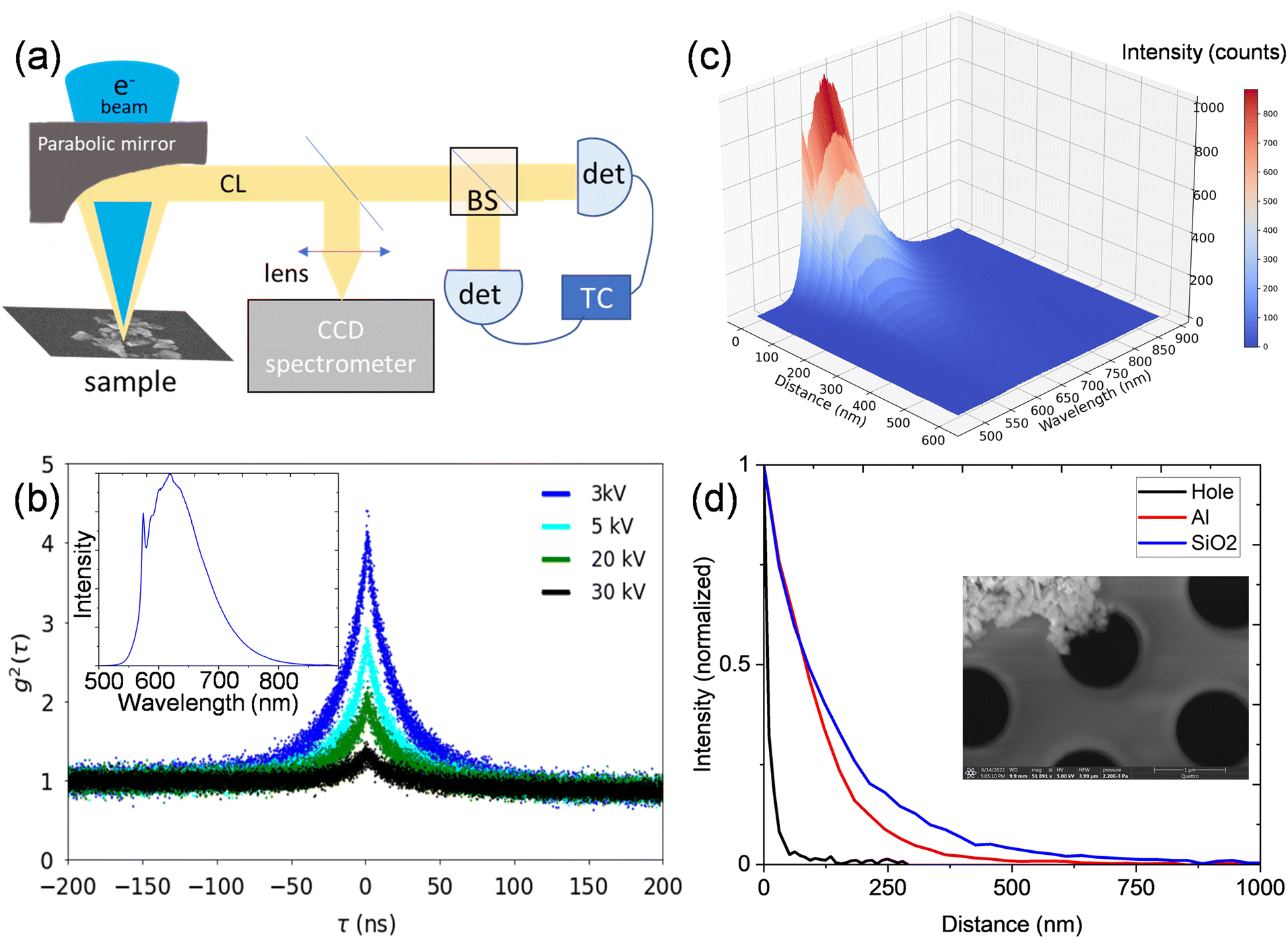 | ||
| Fig. 1 (a) Schematic of CL collection in an SEM, where CL spectrum imaging is performed with a CCD spectrometer and g2(τ) measurement is performed using a beam splitter and two SNSPDs. A time correlator is used to time tag each detected photon. (b) g2(τ) traces taken with electron beam parked on a nanodiamond crystal containing an ensemble of NV centers, showing decreasing bunching with increasing electron beam energy and 4.8 pA current. The inset shows a typical CL spectrum with a peak at 575 nm associated with the NV0 zero-phonon line and a broad phonon sideband at longer wavelengths. No other color centers were observed in any of the CL spectra. (c) Hyperspectral CL as a function of distance from a nanodiamond on an aluminum film at 5 kV and 7 pA. (d) Intensity slice at 625 nm from CL spectra of nanodiamonds on Al and SiO2 and nanodiamonds suspended on a TEM membrane as a function of distance from the nanodiamond (all at 5 kV and 7pA). The inset shows a nanodiamond cluster at the edge of a hole in a SiN membrane. | ||
3 Results
The inset in Fig. 1(b) shows a typical CL spectrum from the nanodiamond, with the distinctive NV0 peak at 575 nm and a broad phonon sideband at longer wavelengths. The NV− peak is suppressed under electron-beam excitation due to beam-induced charge-state conversion.22 No other color centers were observed in any CL spectra. The change in measured bunching as a function of electron-beam energy is shown in Fig. 1(b) for a single nanodiamond crystal on the aluminum film. The bunching decreases with increasing energy at constant 7 pA current, as previously observed in literature.23 The changes in g2(0) can be analytically modeled to assign an effective excitation efficiency as a function of electron beam distance from the nanodiamond. An analytical model developed by Solà-Garcia et al. has been previously used to describe g2(τ) as a function of current, lifetime and excitation efficiency.17 We use that framework here with the assumption that g2(τ) can be fit to a single exponential decay, and we model the second order correlation function as: | (1) |
| γ = 1 − e−b. | (2) |
The energy-dependent bunching seen in Fig. 1(b) can then be understood to result from increasing bulk plasmon excitation efficiency with increasing beam energy, yielding reduced bunching in eqn (1).
We next examine the CL response of a nanodiamond on an aluminum film when the electron beam is not directly incident on the nanodiamond as shown in Fig. 1(c) (where zero distance is defined as the edge of the nanodiamond). The CL intensity decays uniformly over a distance of several hundred nanometers, consistent with a combination of well-understood indirect excitation pathways, including secondary electron excitation, aloof excitation and surface-plasmon-polariton (SPP)-mediated excitation. The efficiency with which Al SPPs directly excite NV centers is expected to be small compared with secondary-electron excitation efficiency, but SPPs do modify the photonic local density of states around the nanodiamond, and can thus introduce a Purcell enhancement of the NV center recombination rate, which should appear as brighter emission and faster recombination rates for nanodiamonds on Al, compared with nanodiamonds on SiO2. The normalized CL intensity at a wavelength of 625 nm is plotted as a function of distance for nanodiamonds on Al and SiO2 films and a holey SiN membrane in Fig. 1(d). The inset shows suspended nanodiamonds on a holey SiN membrane. The length scales for aloof excitations over a SiN hole are substantially smaller than those for secondary-electron mediated excitation, but in each case, substantial CL intensity can be measured with indirect electron-beam excitation.
We investigate the spatially resolved bunching dynamics in a similar fashion, i.e. as a function of electron-beam distance from the nanodiamond. The second order correlation functions measured over a 120 seconds integration time at 4(6) spots for nanodiamonds on Al (SiO2) are shown in Fig. 2(a and b). In both cases, we observe a dramatic increase in g2(0) with increasing distance from the nanodiamond. The NV center lifetime, obtained by fitting each g2(τ) curve with a single exponential decay,15 exhibited no statistically significant dependence on position, with an average value of 25 ± 1 ns on Al and 43 ± 1 ns on SiO2. The lifetimes are similar to those observed previously in literature (NV0 is known to exhibit a longer lifetime than NV−)24,25 and the faster lifetime on the aluminum substrate can be attributed to either a SPP-mediated Purcell enhancement26,27 or to hot-electron transfer between the diamond and the metallic film.28,29 We also collected 2D bunching maps with 25 nm pixel resolution and 10 s per pixel integration times. As shown in Fig. 2(c and d), g2(0) increases exponentially with increasing distance from the nanodiamond (middle panel) and little change was observed in the time constant (lower panel). At electron-beam positions far from the nanodiamond where the total CL counts were too low to reconstruct g2(τ) with sufficient statistical confidence, we left the map blank. The nanodiamonds are located at the bright spots in the panchromatic CL images shown in the top panel of Fig. 2(c and d). Additional g2(τ) maps for nanodiamonds located near the edge of the aluminum film are included in the ESI.‡ Maps of g2(τ) for aloof nanodiamond CL were more challenging to acquire because of the limited spatial extent over which aloof CL can be acquired, but a comparison of the measured bunching in an aloof configuration and under direct electron-beam excitation is also included in the ESI.‡
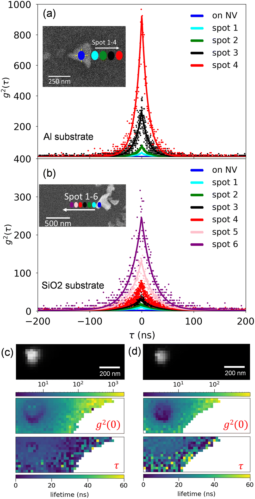 | ||
| Fig. 2 Measured NV CL g2(τ) for various positions on (a and c) Al and (b and d) SiO2 films. The magnitude of g2(0) dramatically increases as the beam moves away from the nanodiamond in both cases. (c) and (d) Show the 2D bunching map collected with 10 s integration per pixel and a 25 nm pixel size, including the panchromatic CL intensity (top panels), the measured CL bunching (middle panels) and the measured bunching time constant (bottom panels). All data was acquired with a 5 kV, 7 pA electron beam. | ||
The top panel of Fig. 3 illustrates the position dependence of NV CL bunching extracted from exponential fits to the g2(τ) shown in Fig. 2(a and b). A least squares fit to the extracted bunching illustrates the exponential growth in the measured bunching as a function of distance from the nanodiamond. On the other hand, the photon counts recorded by the SNSPDs exhibit an exponential decay as shown in the bottom panel of Fig. 3. The position dependent excitation efficiency is calculated from eqn (1) and (2) using the measured bunching and plotted in the inset of Fig. 3 (top panel), demonstrating a clear exponential decay of excitation efficiency with distance. To obtain further insight into the indirect excitation mechanisms, a Monte-Carlo simulation is performed in CASINO to model the density of secondary electrons as a function of distance from the point of excitation.30 The inset in the bottom panel of Fig. 3 depicts the electron trajectories in the simulation. The red trajectories are the electrons that can escape the substrate and excite the nanodiamond. The extracted number of electrons are plotted in grey and scaled to match the counts at 40 nm distance. The position dependence of the number of secondary electrons that interact with the nanodiamond is qualitatively consistent with the position dependence of the NV CL counts. A comparison of the CASINO simulations for electron interactions in both Al and SiO2 substrates is included in the ESI.‡ Critically, we see a greater number of secondary electrons reach the nanodiamond on the SiO2 for a given distance from the nanodiamond (compared with nanodiamonds on the Al film). This increase in effective electron beam current on the SiO2 substrate is consistent with the reduced bunching seen in Fig. 3.
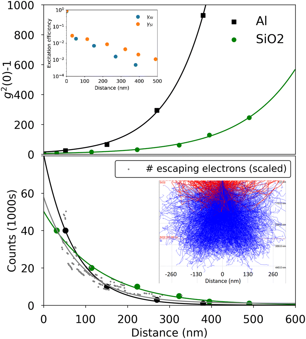 | ||
| Fig. 3 (Top panel) g2(0) as a function of distance from nanodiamonds on Al and SiO2 substrates. The inset shows the excitation efficiency, γ calculated from the measured bunching using eqn (1) and (2). (Bottom panel) Single channel CL counts per s. The solid lines are exponential fits. (Inset of bottom panel) Electron trajectories in SiO2 from CASINO Monte-Carlo simulation, where red trajectories illustrate the escaping secondary electrons. The number of escaping electrons (scaled) as a function of distance is shown in grey, with a fit to the modeled data again shown with a solid line. All data was acquired with a 5 kV, 7 pA electron beam. | ||
Finally, we investigated the current and voltage dependence of g2(τ) for an electron beam parked at a fixed distance of 30 nm from the nanodiamond on the SiO2 substrate. We found increasing g2(0) with decreasing current (Fig. 4(a)), as observed previously in literature, and consistent with the understanding that, at high currents, the CL photon statistics are dominated by the Poissonian electron distribution while at low currents, the CL photon statistics are dominated by the impulsive excitation of ensembles of emitters by each electron. However, we also observed increasing g2(0) with increasing voltage (Fig. 4(b)), in marked contrast to previous reports in the literature and to measurements reported here with the electron-beam directly incident on the nanodiamond, as shown in Fig. 1(b).16
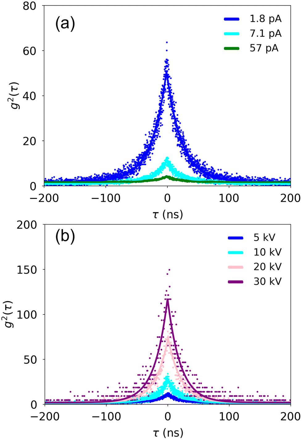 | ||
| Fig. 4 (a) Current dependence at 5 kV accelerating voltage and (b) accelerating voltage dependence at ∼10 pA of g2(τ) for electron beam parked at 30 nm distance from the nanodiamond on the SiO2 substrate. | ||
This seemingly anomalous scaling can be considered separately for the aloof-excitation regime and for the secondary-electron excitation regime. When a nanodiamond is directly irradiated by high energy electrons, its bulk plasmon mode exhibits a large cross section for excitation through momentum-transferring inelastic scattering processes between the incident electron and the nanodiamond-bound electrons. The excited bulk plasmon mode will decay by way of inelastic scattering processes between the electrons associated with the plasmon mode and the other electrons (and nuclei) comprising the nanodiamond. In this way, plasmons excited in the nanodiamond due to the passage of external electrons through their bulk excite ensembles of NV centers, which can then decay radiatively through CL. The same plasmon-mediated NV-centered excitation pathway can also occur when the external electrons that traverse the interior of the nanodiamond are not the primary electrons comprising the beam, but are instead secondary electrons ejected from the substrate in the direction of the nanodiamond. The excitation of plasmons by these secondary electrons is, for example, responsible for the behavior observed in Fig. 1(d) for the position-dependent CL intensity from substantially identical nanodiamonds deposited onto continuous substrates versus those suspended over a hole in a TEM membrane. This secondary electron excitation mechanism is phenomenologically comparable to the existing plasmon-mediated excitation process described in eqn (1) and (2), but the effective electron-beam current at the nanodiamond falls off with increasing distance.
In contrast to the case presented above where a sufficiently-energetic primary/secondary electron penetrates the volume of the nanodiamond, the so-called “optical” (i.e., zero momentum transfer limit) selection rules for electronic excitations take effect when primary/secondary electrons pass outside of the volume of the nanodiamond. Under these conditions, excitation of the diamond bulk plasmon mode is forbidden. However, NV centers can still be directly excited in this case by the evanescent electric field from a primary/secondary electron passing outside of the nanodiamond, with the probability of inducing a given excitation (within the electric-dipole approximation31) proportional to the squared modulus of the inner product between its associated transition dipole moment and the electric field emanated by the distant beam. The aloof excitation efficiency is expected to be most prominent for primary and secondary electrons incident within 10–20 nm of the nanodiamond, so the position-dependent excitation efficiency illustrated in Fig. 1(d) for nanodiamonds adjacent to a hole in a SiN membrane is determined by this aloof excitation mechanism, while the nanodiamonds on bulk substrates are excited by a combination of aloof excitation from primary and secondary electrons and from secondary electrons that hit the nanodiamond and excite the bulk plasmon directly. Because of the excitation efficiency of bulk plasmons and the diameter of the nanodiamonds relative to the aloof interaction cross-section, we assume that “direct” secondary-electron excitation is the primary contribution to the NV center CL seen for nanodiamonds on bulk substrates when the electron beam is not directly incident on the nanodiamond.
With the distance dependence of the relative contribution of different pathways for exciting the NV-center transitions established, we are equipped to rationalize the behavior of g2(0) with increasing beam energy observed in Fig. 4(b). An increase in total CL intensity from an ensemble of quasi-impulsively excited color centers will be observed with increasing aloof beam energy due to the electric field emanated by the beam electrons becoming stronger in the directions transverse to their motion (a consequence of relativistic length contraction that is described for a charged particle undergoing uniform motion within the Liénard–Wiechert formalism32). Since higher-energy aloof electron beams will excite an ensemble of color centers in a nearby nanodiamond with greater efficiency (due to the increased beam–matter interaction strength described above), and more concurrently (due to the increasingly local-in-time nature of the perturbation) than lower-energy ones, brighter and increasingly bunched CL can be anticipated a priori for higher-energy aloof irradiation. On the other hand, secondary electrons that hit the nanodiamond “directly” after being excited in the substrate some distance from the nanodiamond can excite diamond bulk plasmon modes, but the effective current at the nanodiamond will decay exponentially with increasing beam energy, as shown in the ESI.‡ It then follows directly that the bunching expected in eqn (1) will climb exponentially with increasing beam energy as a result of the decay in the effective electron-beam current. This model treats the secondary-electron energy dependence of the plasmon excitation efficiency as a second order effect, but such effects could be included for a more quantitative picture of the spatially dependent bunching generated by indirect electron-beam excitation.
4 Conclusion
In conclusion, a clear understanding of indirect electron-beam excitation processes is critical to the understanding of CL g2(τ) microscopies. We found that the measured bunching increases exponentially as the electron beam is moved away from an ensemble of emitters, with a corresponding exponential decrease in the total number of counts measured. The distance dependence of the bunching is consistent with a reduced effective electron-beam current for secondary electrons that hit the nanodiamond after scattering in the substrate, though aloof interactions introduce a similar effect at shorter length scales. Cathodoluminescence microscopies have become increasingly critical tools for probing beam-sensitive 2D materials33,34 and perovskite films.35,36 The ability to probe nanoscale excited state dynamics in these materials without direct electron-beam excitation will enable new CL imaging modalities that would otherwise introduce unmanageable beam-induced damage due to excessive dwell times.Conflicts of interest
There are no conflicts to declare.Acknowledgements
This research was supported by the Center for Nanophase Materials Sciences, which is a U.S. Department of Energy Office of Science User Facility and by the U. S. Department of Energy, Office of Science, Basic Energy Sciences, Materials Sciences and Engineering Division. J. N. was supported by the U.S. Department of Energy, Office of Science, Office of Workforce Development for Teachers and Scientists (WDTS) under the Science Undergraduate Laboratory Internship program.Notes and references
- F. J. Garcìa de Abajo and V. Di Giulio, ACS Photonics, 2021, 8, 945–974 CrossRef PubMed.
- F. Hayee, L. Yu, J. L. Zhang, C. J. Ciccarino, M. Nguyen, A. F. Marshall, I. Aharonovich, J. Vučković, P. Narang, T. F. Heinz and J. A. Dionne, Nat. Mater., 2020, 19, 534–539 CrossRef CAS PubMed.
- M. Kuttge, E. J. R. Vesseur, A. F. Koenderink, H. J. Lezec, H. A. Atwater, F. J. García de Abajo and A. Polman, Phys. Rev. B: Condens. Matter Mater. Phys., 2009, 79, 113405 CrossRef.
- D. A. Garfinkel, V. Iyer, R. Seils, G. Pakeltis, M. R. Bourgeois, A. W. Rossi, C. Klein, B. J. Lawrie, D. J. Masiello and P. D. Rack, ACS Appl. Nano Mater., 2022, 5, 1798–1807 CrossRef CAS.
- T. Sannomiya, A. Konecna, T. Matsukata, Z. Thollar, T. Okamoto, F. J. García de Abajo and N. Yamamoto, Nano Lett., 2019, 20, 592–598 CrossRef PubMed.
- J. A. Hachtel, S.-Y. Cho, R. B. Davidson, M. A. Feldman, M. F. Chisholm, R. F. Haglund, J. C. Idrobo, S. T. Pantelides and B. J. Lawrie, Light: Sci. Appl., 2019, 8, 1–9 CrossRef CAS PubMed.
- V. Iyer, Y. S. Phang, A. Butler, J. Chen, B. Lerner, C. Argyropoulos, T. Hoang and B. Lawrie, APL Photonics, 2021, 6, 106103 CrossRef CAS.
- S. Meuret, L. H. G. Tizei, F. Houdellier, S. Weber, Y. Auad, M. Tencé, H.-C. Chang, M. Kociak and A. Arbouet, Appl. Phys. Lett., 2021, 119, 062106 CrossRef CAS.
- N. Varkentina, Y. Auad, S. Y. Woo, A. Zobelli, L. Bocher, J.-D. Blazit, X. Li, M. Tencé, K. Watanabe and T. Taniguchi, et al. , Sci. Adv., 2022, 8, eabq4947 CrossRef CAS PubMed.
- C. Dıaz-Guerra, J. Piqueras, A. Castaldini, A. Cavallini and L. Polenta, J. Appl. Phys., 2003, 94, 2341–2346 CrossRef.
- M. Merano, S. Sonderegger, A. Crottini, S. Collin, P. Renucci, E. Pelucchi, A. Malko, M. H. Baier, E. Kapon, B. Deveaud and J.-D. Ganière, Nature, 2005, 438, 479–482 CrossRef CAS PubMed.
- R. J. Moerland, I. G. C. Weppelman, M. W. H. Garming, P. Kruit and J. P. Hoogenboom, Opt. Express, 2016, 24, 24760–24772 CrossRef CAS PubMed.
- M. Solà-Garcia, PhD thesis, University of Amsterdam, 2021 Search PubMed.
- D.-S. Yang, O. F. Mohammed and A. H. Zewail, Proc. Natl. Acad. Sci. U. S. A., 2010, 107, 14993–14998 CrossRef CAS PubMed.
- S. Meuret, M. Solà Garcia, T. Coenen, E. Kieft, H. Zeijlemaker, M. Ltzel, S. Christiansen, S. Woo, Y. Ra, Z. Mi and A. Polman, Ultramicroscopy, 2019, 197, 28–38 CrossRef CAS PubMed.
- S. Meuret, L. H. G. Tizei, T. Cazimajou, R. Bourrellier, H. C. Chang, F. Treussart and M. Kociak, Phys. Rev. Lett., 2015, 114, 197401 CrossRef CAS PubMed.
- M. Solà-Garcia, K. W. Mauser, M. Liebtrau, T. Coenen, S. Christiansen, S. Meuret and A. Polman, ACS Photonics, 2021, 8, 916–925 CrossRef PubMed.
- M. A. Feldman, E. F. Dumitrescu, D. Bridges, M. F. Chisholm, R. B. Davidson, P. G. Evans, J. A. Hachtel, A. Hu, R. C. Pooser, R. F. Haglund and B. J. Lawrie, Phys. Rev. B, 2018, 97, 081404 CrossRef CAS.
- S. Meuret, T. Coenen, S. Y. Woo, Y.-H. Ra, Z. Mi and A. Polman, Nano Lett., 2018, 18, 2288–2293 CrossRef CAS PubMed.
- L. Zhang, R. Erni, J. Verbeeck and G. Van Tendeloo, Phys. Rev. B: Condens. Matter Mater. Phys., 2008, 77, 195119 CrossRef.
- L. H. G. Tizei and M. Kociak, Nanotechnology, 2012, 23, 175702 CrossRef CAS PubMed.
- M. Solà-Garcia, S. Meuret, T. Coenen and A. Polman, ACS Photonics, 2020, 7, 232–240 CrossRef PubMed.
- S. Meuret, T. Coenen, H. Zeijlemaker, M. Latzel, S. Christiansen, S. Conesa-Boj and A. Polman, Phys. Rev. B, 2017, 96, 035308 CrossRef.
- G. Liaugaudas, G. Davies, K. Suhling, R. U. A. Khan and D. J. F. Evans, J. Phys.: Condens. Matter, 2012, 24, 435503 CrossRef CAS PubMed.
- J. Storteboom, P. Dolan, S. Castelletto, X. Li and M. Gu, Opt. Express, 2015, 23, 11327–11333 CrossRef CAS PubMed.
- H. Li, J. Y. Ou, B. Gholipour, J. K. So, D. Piccinotti, V. A. Fedotov and N. Papasimakis, Appl. Phys. Lett., 2021, 118, 261103 CrossRef CAS.
- S. Yanagimoto, N. Yamamoto, T. Sannomiya and K. Akiba, Phys. Rev. B, 2021, 103, 205418 CrossRef CAS.
- S. Wieghold and L. Nienhaus, Joule, 2020, 4, 524–538 CrossRef CAS.
- B. Lawrie, R. Haglund and R. Mu, Opt. Express, 2009, 17, 2565–2572 CrossRef CAS PubMed.
- D. Drouin, P. Hovington and R. Gauvin, Scanning, 1997, 19, 20–28 CrossRef CAS.
- G. C. Schatz and M. A. Ratner, Quantum Mechanics in Chemistry, Courier Corporation, 2002 Search PubMed ch. 5.
- R. Feynman, R. Leighton and M. Sands, The Feynman Lectures on Physics: Mainly Electromagnetism and Matter, Addison-Wesley Publishing Company, 1965, ch. 26 Search PubMed.
- G. Nayak, S. Lisi, W. Liu, T. Jakubczyk, P. Stepanov, F. Donatini, K. Watanabe, T. Taniguchi, A. Bid, J. Kasprzak, M. Richard, V. Bouchiat, J. Coraux, L. Marty, N. Bendiab and J. Renard, Phys. Rev. Mater., 2019, 3, 114001 CrossRef CAS.
- D. Curie, J. T. Krogel, L. Cavar, A. Solanki, P. Upadhyaya, T. Li, Y.-Y. Pai, M. Chilcote, V. Iyer, A. Puretzky, I. Ivanov, M.-H. Du, F. Reboredo and B. Lawrie, ACS Appl. Mater. Interfaces, 2022, 14, 41361–41368 CrossRef CAS PubMed.
- C. Xiao, Z. Li, H. Guthrey, J. Moseley, Y. Yang, S. Wozny, H. Moutinho, B. To, J. J. Berry, B. Gorman, Y. Yan, K. Zhu and M. Al-Jassim, J. Phys. Chem. C, 2015, 119, 26904–26911 CrossRef CAS.
- E. J. Taylor, V. Iyer, B. S. Dhami, C. Klein, B. J. Lawrie and K. Appavoo, 2022, preprint, arXiv:2201.06546. DOI:10.48550/arXiv.2201.06546.
Footnotes |
| † This manuscript has been authored by UT-Battelle, LLC, under contract DE-AC05-00OR22725 with the US Department of Energy (DOE). The US government retains and the publisher, by accepting the article for publication, acknowledges that the US government retains a nonexclusive, paid-up, irrevocable, worldwide license to publish or reproduce the published form of this manuscript, or allow others to do so, for US government purposes. DOE will provide public access to these results of federally sponsored research in accordance with the DOE Public Access Plan (https://energy.gov/downloads/doe-public-access-plan). |
| ‡ Electronic supplementary information (ESI) available. See DOI: https://doi.org/10.1039/d3nr00376k |
| This journal is © The Royal Society of Chemistry 2023 |