
 Open Access Article
 This Open Access Article is licensed under a
 Creative Commons Attribution 3.0 Unported Licence
Stacking influence on the in-plane magnetic anisotropy in a 2D magnetic system
Sandra
Ruiz-Gómez
a,
Lucas
Pérez
bcd,
Arantzazu
Mascaraque
bc,
Benito
Santos
ef,
Farid
El Gabaly
 g,
Andreas K.
Schmid
h and
Juan
de la Figuera
*i
g,
Andreas K.
Schmid
h and
Juan
de la Figuera
*i
aMax-Planck-Institut für Chemische Physik fester Stoffe, 01187 Dresden, Germany
bDept. Física de Materiales, Universidad Complutense de Madrid, 28040 Madrid, Spain
c“Surface Science and Magnetism of Low Dimensional Systems”, UCM, Unidad Asociada al IQFR-CSIC, 28040 Madrid, Spain
dIMDEA Nanociencia, 28049 Madrid, Spain
eInstituto Regional de Investigación Científica Aplicada (IRICA), 13005 Ciudad Real, Spain
fDept. Física Aplicada, Universidad de Castilla-La Mancha, 13071 Ciudad Real, Spain
gSandia National Laboratories, Livermore, California 94550, USA
hLawrence Berkeley National Laboratory, Berkeley, California 94720, USA
iInstituto de Química-Física “Rocasolano”, CSIC, Madrid 28006, Spain. E-mail: juan.delafiguera@csic.es; Tel: +34 91 745 9517
First published on 11th April 2023
Abstract
The magnetization patterns on three atomic layers thick islands of Co on Ru(0001) are studied by spin-polarized low-energy electron microscopy (SPLEEM). In-plane magnetized micrometer wide triangular Co islands are grown on Ru(0001). They present two different orientations correlated with two different stacking sequences which differ only in the last layer position. The stacking sequence determines the type of magnetization pattern observed: the hcp islands present very wide domain walls, while the fcc islands present domains separated by much narrower domain walls. The former is an extremely low in-plane anisotropy system. We estimate the in-plane magnetic anisotropy of the fcc regions to be 1.96 × 10⁴ J m−3 and of the hcp ones to be 2.5 × 10² J m−3.
1 Introduction
Two-dimensional magnetism1 has a rich history that started in the first part of the XXth century with the discussion of the Heisenberg and Ising Hamiltonians.2 Further theoretical developments included the Mermin–Wagner theorem that precluded long-range order for an isotropic system.3 The experimental realization of a two-dimensional magnetic system involves three distinct families of materials, which are chronologically described in ref. 1: (i) quasi-2D magnetism in bulk compounds with weak interlayer interactions, first discussed in the 50s, (ii) Fe, Co and Ni metallic ultrathin films (down to a single atomic layer4,5) on different single crystal metallic substrates, where magnetic order was first observed in the early 90s, and (iii) van der Waals materials showing ferromagnetic ordering, discovered in the last decade. The latter field has been growing rapidly in the last few years.6 These 2D magnets show exotic physical phenomena as well as the possibility of tuning magnetism by electric fields, strain, chemical functionalization or stacking engineering.7 Most of these materials are layered, cleavable transition-metal chalcogenides and halides; so, although very interesting from the fundamental point of view, these materials are not currently easy to grow and integrate on top of spintronic devices.8 Thus, the realization of 2D magnetic systems consisting of metallic films a few atoms thick supported by non-magnetic materials remains an active field of research. In fact, we note that such systems have been originally proposed as the best realization of 2D ferromagnets with exact XY symmetry.9The control of magnetism in these ultrathin metal films is governed by magnetic anisotropy, whose physical origin lies in the competition between the magnetic dipolar interaction and the spin–orbit interaction that gives rise to the magnetocrystalline anisotropy. Although the magnetic anisotropy energy is larger in thin films and surfaces than in bulk materials,10 in the former case it is still only a few meV per atom. It can thus be readily modified by strain,11 temperature,12 or adsorbates,13–17 providing tools to control the magnetization.
Here we study the case of 3-atoms thick cobalt films supported on a Ru(0001) substrate. Cobalt layers a few atoms thick on Ru(0001) are 2D-magnetic systems that present long range order: a film one atomic layer thick has a Curie temperature of 200 K and in-plane magnetization, films two atoms thick have a Curie temperature of 500 K and out-of-plane magnetization, and films three atoms thick have again an in-plane magnetization and a Curie temperature above 600 K.5Ab initio calculations5,18 have shown that the spin reorientation transitions arise from a combination of strain and surface effects. Recent work has taken advantage of the low magnetocrystalline anisotropy of the monolayer-thick Co films on Ru(0001) to study skyrmion formation under low magnetic fields19,20 or even proximity superconductivity effects,21 promoting Co films a few atomic layers thick on ruthenium as a novel quantum material.
Bulk cobalt presents two different close-packed crystal structures: hcp at low temperatures and fcc at higher temperatures. The transition between them, at a temperature of 690 K, is a classic martensitic transformation.22 The low transition temperature is reflected in the low stacking fault energy in both structures.23 It has been noted long ago that the grain size affects the stable structure.24 When growing Co on single crystal metal substrates, it is not uncommon to obtain a different stacking sequence from the bulk hcp. For example, films of tens of atomic layers on Pt(111) present an fcc stacking sequence.25 Thus, cobalt layers a few atoms thick are an excellent system to study the effect of stacking in a 2D system. Up to two layers, Co films on Ru present only one stacking sequence. Regions one and two atoms thick follow the Ru hcp stacking sequence. Using the ABC naming scheme for the possible position of each hexagonal layer, the stacking sequence on a given Ru terrace can be described as abA and abAB respectively for one and two-layer regions, with lower case indicating the Ru layers, and upper case the Co layers (we are disregarding here the presence of a moiré pattern between the Ru substrate and the Co layers for regions thicker than one atom).26 However, on islands three atoms thick the top layer can be located in two different positions:26 either abABC or abABA sequences can be found. The first case corresponds to an fcc sequence, while the second corresponds to an hcp sequence. As both islands have the same strain state, this opens up the way to study the effect of the stacking sequence on the magnetic properties in the thinnest possible system where such a stacking difference between hexagonal layers can exist.
In this work, we explore the dependence of the magnetic texture on the stacking sequence for 3-atoms-thick Co regions by spin-polarized low-energy electron microscopy (SPLEEM27), finding that the effective anisotropy changes by two orders of magnitude.
2 Experimental methods
The experiments have been performed using a spin-polarized electron microscope (SPLEEM28) of the National Center for Electron Microscopy, part of the Molecular Foundry in the Lawrence Berkeley National Laboratory. This instrument29 allows acquisition of low-energy electron images with magnetic contrast using a spin-polarized electron beam for illumination, whose spin orientation can be selected along any desired direction.30 The base pressure of the main chamber, where the growth of the Co films takes place under observation in real time by SPLEEM,31 is in the low 10−11 mbar. The Ru(0001) single crystal substrate has been cleaned by repeated cycles of consecutive exposures to oxygen and flashing to 1700 K. Before cobalt growth, the sample was flashed several times in vacuum to remove all the oxygen. The cleanliness of the films was checked by Auger electron spectroscopy. The growth has also been performed using the same recipe in synchrotron experiments in the past,32 where neither contamination nor oxidation was detected by X-ray absorption spectroscopy. Cobalt films have been grown from a doser with a Co rod heated by electron bombardment inside a cooling water jacket, with the pressure remaining below 7 × 10⁻¹¹ mbar. The doser is calibrated by measuring the time required to complete the first layer of cobalt on ruthenium.26 The typical flux is one (atomic) monolayer (ML) every 3 minutes. The growth temperature was 600 K, measured using a type C thermocouple. All observations have been performed in situ.Micromagnetic simulations were performed with the MuMax3 software33 using an Nvidia GeForce GTX 1660 Ti with 6 GB. The simulations were performed in a slab with typical voxel sizes of 1 nm × 1 nm × 0.6 nm. For the simulation of the experimental magnetic texture, the geometry was taken from the experimental images and the voxel size was 2.8 nm × 2.8 nm × 0.2 nm. The choices of material parameters are discussed when the simulation results are presented.
3 Results
At the growth temperature employed, cobalt on Ru(0001) grows layer-by-layer in the form of triangular islands coalescing into complete layers.26 The in-plane lattice spacing of films thicker than a single layer is relaxed close to the Co-bulk value. Relative to the underlying Ru there are different absorption sites for the 1st cobalt layer atoms in multilayer films, mostly hcp and fcc but also bridge and on-top positions, as shown by the presence of a moiré pattern.26 But within the film itself, there is only one stacking sequence up to a thickness of two monolayers.34 Three atom-thick islands can be grown to be up to several micrometer wide.32 Those islands present two different stacking sequences reflected by the in-plane orientation of their triangular shape:26 islands with different stacking sequences are outlined green and red in Fig. 1(a). | ||
| Fig. 1 (a) LEEM image with a 12 μm field of view (FOV) from a film of Co on Ru(0001). The two types of islands with different stacking sequences—hcp and fcc—are outlined in red and green respectively. (b) SPLEEM image of the same area, corresponding to in-plane magnetization. The sample is imaged at 400 K. | ||
The two different stacking sequences (indicated in the schematic of Fig. 2) are named ABC (for the fcc stacking sequence) and ABA (for the hcp stacking sequence). They have been identified in ref. 26 using low-energy electron diffraction (LEED) intensity vs. energy curves acquired from each island type, by comparison with multiple scattering calculations, and correlated with their triangular orientation. Furthermore, the two types of islands have different electron reflectivities at particular energies acquiring images with the specular beam. It has also been found that the islands that grow from the step edges present preferentially an hcp stacking sequence. SPLEEM microscopy used in the present work does not allow acquisition of selected area diffraction patterns, so the identification of each island type relies on the electron reflectivity differences and the identification of the shape of islands grown from the step edges.
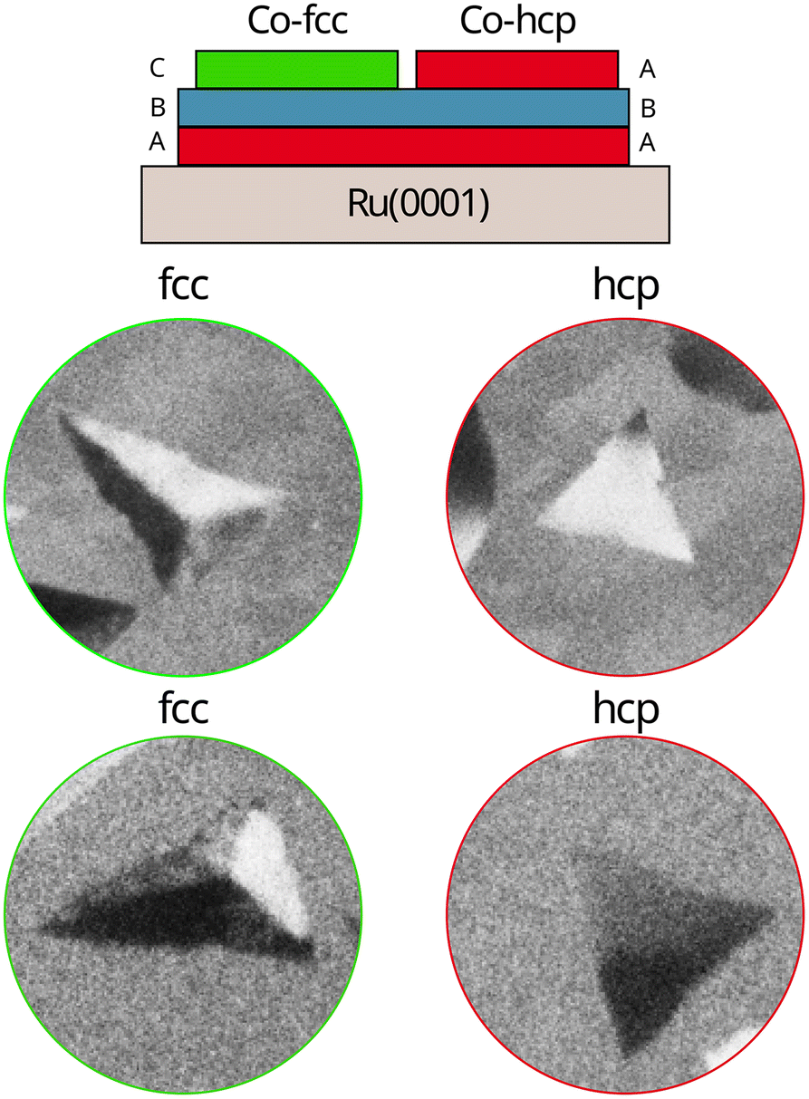 | ||
| Fig. 2 Top: schematic of the fcc and hcp growth stacking sequences of 3 ML cobalt islands. SPLEEM images of several islands. Top row: fcc and hcp islands, respectively, on the same substrate terrace. Bottom row: fcc and hcp islands on another Ru terrace where the orientation of the islands is different. All the images are acquired with a start voltage of 7.5 eV and correspond to a FOV of 2.8 μm. The sample is imaged at 400 K. | ||
Strain effects are often relevant for nanostructures35 and ultrathin films alike. In fact, the spin-orientation for a Co layer film can only be explained by the expanded lattice parameter of that single layer when compared with bulk Co.5 The strain state of the two islands can be obtained from the LEED patterns acquired from each type of island:26 within the experimental error, both types have the same lattice parameter and thus have the same strain state. This is not unexpected, as they share the same underlying two layers.
We use spin-polarized LEEM (SPLEEM) to determine the magnetization pattern in remanence (i.e. with no applied magnetic field) on each type of island. In SPLEEM, a spin-polarized electron beam is used to acquire low-energy electron microscopy (LEEM31) images.27 As described in detail in our published work,5,34,36 the pixel-by-pixel asymmetry between the LEEM images acquired with opposite spin-polarization provides a nanometer-resolution map of the component of the magnetization along the selected spin-direction: bright (dark) areas indicate that the local surface magnetization has a component parallel (anti-parallel) to the spin-polarization direction of the electron beam, while gray areas signal a zero magnetization component. In particular, the magnetization component imaged in the presented SPLEEM images corresponds to a direction rotated 33° counterclockwise of the y-axis of the figure. The area surrounding the islands is covered with a complete film 2 ML thick. Those areas are magnetized with the easy-axis out-of-plane, as observed in the SPLEEM images with out-of-plane contrast, in agreement with previous reports.5 They thus appear gray in Fig. 1(b) or 2. The domain patterns observed on the 3 ML Co islands belong to two different classes. One is a pattern composed of domains separated by narrow domain walls between them, often dividing each triangle into three regions, as shown in the two images on the left side of Fig. 2. The other class comprises either single domain islands or islands with a very wide domain wall, as shown in the right side of Fig. 2.
Although in Fig. 1 it would seem that the correlation is between the island orientation and the magnetization pattern, we show in Fig. 2 that the correlation is not with the orientation itself, but rather with the island stacking sequence. On Ru(0001) the substrate termination changes at consecutive terraces due to its hcp stacking sequence,37 so the particular identification of islands with a given orientation changes from terrace to terrace.5,38 Nevertheless, we have shown that the particular stacking sequence of each island can be determined by LEEM images at particular electron energies and by comparison with the shapes of islands growing from an upper substrate step.26 In the images presented in Fig. 2, the top row islands are on the same substrate terrace, and the lower ones are on a different substrate terrace. Moving from one terrace to another one where the fcc islands have a different orientation (compare the left upper image of Fig. 2 with the left lower one), the pattern is still composed of sharp domain walls. Likewise for the hcp islands: the two islands on the right hand side of Fig. 2 are nearly single domains irrespective of their particular orientation.
In all cases, the walls are of the Néel type: the magnetization is always within the film plane. This is to be expected given that the thickness of those areas is 0.6 nm (3 atomic layers). In the fcc islands (left column in Fig. 2) the domain walls observed have a typical width of 0.24 ± 0.02 μm. In the hcp islands, the domain wall width is comparable in size with the islands, giving rise to either single domain islands or, at most, islands with a wide domain wall that occupies most of the island (see the right side of Fig. 2). We note that in all cases the width of the walls is much larger than for bulk Bloch walls in Co (∼30 nm![[thin space (1/6-em)]](https://www.rsc.org/images/entities/char_2009.gif) 39).
39).
The domains in the fcc islands, as shown in Fig. 2, resemble closure domains where the magnetization follows the sides of the islands, as observed in magnetite islands.40 However, we need to consider not one component but the full vector of the magnetization. As SPLEEM allows us to change the illumination electron beam spin direction, we can reconstruct the vector magnetization by measuring SPLEEM images with the spin direction along three non-coplanar directions. The vector magnetization is shown in Fig. 3a using a hue scale for the in-plane direction and saturation for the out-of-plane component. The 2 ML areas have out-of-plane magnetization. The domains of the 3 ML islands, instead, are in-plane.5 The domain pattern in the fcc island is not a closure domain, and the magnetization direction in each domain is not parallel to each side. For single domain islands, the magnetization vector in the out-of-plane magnetization of the 2-layer thick surrounding area is such as to close the magnetic flux that arises from the 3-layer island.
 | ||
| Fig. 3 (a) Reconstruction of the vector magnetization from the images acquired at three orthogonal directions. (b) Micromagnetic simulation relaxing the experimental configuration presented in (a). The SPLEEM images were measured at a sample temperature of 387 K. | ||
4 Discussion
We have observed that the domain wall width thus depends on the stacking sequence in 3 ML thick islands. What is the origin of such a difference? The domain wall width is determined by the ratio of the exchange stiffness and the effective in-plane magnetic anisotropy. The effective in-plane anisotropy in such thin films is typically a combination of interface and magnetocrystalline anisotropies.The exchange stiffness Aex itself is not expected to depend strongly on the stacking sequence. Moreno et al.39 in particular searched for a possible dependence of the exchange stiffness on the stacking sequence39 and none was found. We thus assume that both the hcp and the fcc islands have the same exchange stiffness. The change in the domain wall width should then arise because of changes in the in-plane anisotropy. We further note that the interface or other anisotropies should be the same in the two types of islands, as the lower two layers and the interface with the Ru are identical, as well as their strain states.26 Thus the differences should arise specifically from a dependence of the magnetocrystalline anisotropy on the stacking sequence of the last Co layer.
While it might be surprising that the magnetocrystalline anisotropy would change so much with the change in the stacking of a single atomic layer, such a large difference is suggested from the differences between bulk fcc and hcp Co magnetocrystalline anisotropies. Hcp Co has a strong uniaxial anisotropy in the direction perpendicular to the basal (0001) plane, of the order of K1 ∼ 4.5 × 10⁵ J m−3.41 Within the basal plane, the first magnetocrystalline anisotropy is the fourth order term which has an in-plane six-fold symmetry, K4sin6θcos6ϕ, with θ being the polar angle and ϕ the azimuthal one. At room temperature, K4 is 5.5 × 10³ J m−3.41 Fcc Co, on the other hand, is a cubic structure that has a substantial first order anisotropy of Kc1 = −2.7 × 10⁴ J m−3.42 So it is reasonable to expect that the effective in-plane anisotropy might be lower for the hcp than for the fcc islands.
However, it is known that the magnetocrystalline anisotropies in the bulk can differ substantially from the ones for ultrathin films. Furthermore, effective anisotropy includes also interface or surface terms. So we proceed to obtain them from the experimental observations. In order to do so, we first need the exchange stiffness for a 3 ML thick Co film. We use as the starting point the value obtained by Moreno et al.39 for bulk Co. For 2 ML and 3 ML regions, we scale the bulk value39 by the ratio of the Curie temperature of each region to the 1400 K bulk value. The Curie temperature for the 1 ML region is 200 K.5 For the 2 ML region we have measured that the Curie temperature is 500 K.5 We lack an experimental estimate of the 3 ML case, as we only know that it is higher than 600 K. However, at higher temperatures dewetting and alloying already take place in the Co–Ru system.26 So instead of measuring it experimentally, we assume a linear dependence on the number of layers, following Schneider et al.4 This provides an estimate of the Curie temperature for 3 ML regions of 800 K. We thus estimate the exchange stiffness for 2 and 3 ML regions to be 1.28 × 10⁻¹¹ J m−1 and 2.05 × 10⁻¹¹ J m−1 respectively.
In the absence of experimental data, we assume that the saturation magnetization should be the same through the film, and we set it to the bulk value of 1.83 T, i.e. MS = 1.46 × 10⁶ A m−1.43
In the case of fcc islands for which the domain walls are well defined, we can use the classic dependence  . However, such expression is only valid for thicker films. To minimize the magnetostatic energy of the wall with decreasing film thickness, the Néel wall width increases.44 In order to determine the proper relationship, we perform micromagnetic simulations on a rectangular slab, 4 μm long and 0.5 μm wide. The cell height of the simulation corresponds to the thickness of the experimental film (0.6 nm), while the in-plane size has been selected to be 1 nm wide. The material parameters used were MS = 1.46 × 10⁶ A m−1 and Aex = 2.05 × 10⁻¹¹ J m−1. The cubic in-plane anisotropy was varied until the experimental domain width of 0.24 μm was obtained. The required in-plane anisotropy was found to be 1.96 × 10⁴ J m−3. If we consider that our islands present a (111) orientation with the sides along the 〈110〉 in-plane directions, the cubic anisotropy axis would be along the 〈111〉 directions, which makes a 19° angle with the plane. Thus, we estimate the cubic anisotropy to be 2.1 × 10⁴ J m−3, which is surprisingly similar to the bulk value (2.7 × 10⁴ J m−3 (ref. 42)) even if the domain wall width is an order of magnitude larger than that for bulk Co,39 highlighting the role of the magnetostatic energy in determining the wall width in such an ultra-thin system.
For the hcp islands, the domain wall width is not well defined, other than being of the order of the island size. Using the same micromagnetic calculation would give an in-plane anisotropy of the order of 103 J m−3 for a micron-sized domain wall. For lower anisotropies, the system relaxes to a single domain state in the micromagnetic simulation. To provide an alternative way of estimating the anisotropy in the hcp islands, we use the fluctuations that have been observed in the domains on the hcp islands upon increasing the temperature. While for 400 K no changes in the domains are observed (see Fig. 1), for a temperature of 500 K (Fig. 4) we observed changes in the domains within 10 s. We then use the classic estimate of the switching time τ of a magnetic particle τs/τ0 = exp(KeffV/kBT), with T as the measurement temperature, V as the volume of the island, τ0 as an attempt frequency of the order of 10−10 s, and kB as the Boltzmann constant. This provides an estimate of Keff = 2.5 × 10² J m−3. The effective anisotropy of the hcp islands is nearly two orders of magnitude smaller than that of the fcc islands. Even if it is not zero, this might well be one of the systems that more closely resembles the prediction of the lack of magnetic anisotropy in a hexagonal 2D magnetic system, put forward by Pokrovsky and others.9
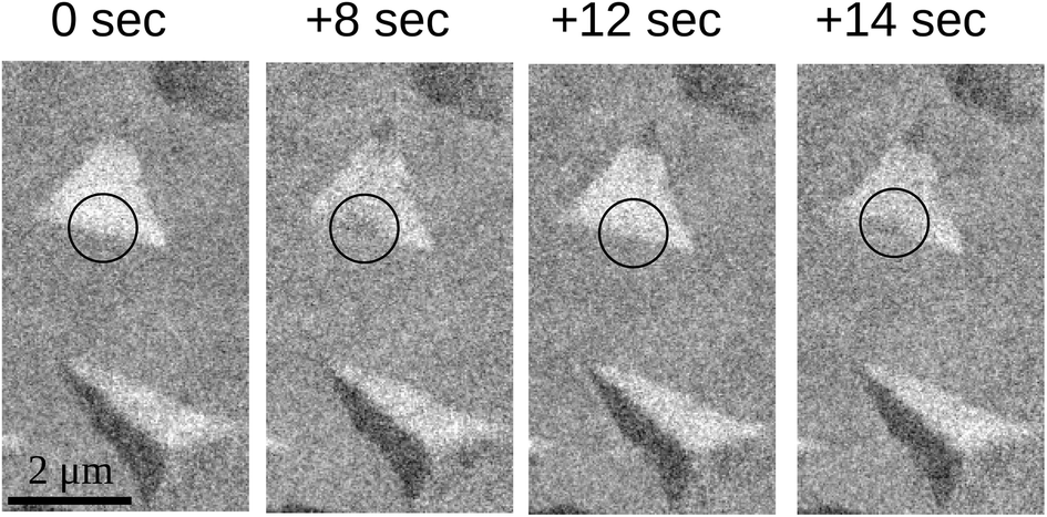 | ||
| Fig. 4 SPLEEM images at a temperature of 500 K with in-plane contrast along an angle of 135°. A fluctuating domain is marked with a circle in an hcp island. | ||
Using those material parameters, we carried out a micromagnetic simulation for a region with the same dimensions as the experimental one shown in Fig. 3a. The cell in-plane width was 2.8 nm and the cell height has been set to 0.2 nm, in order to use two cells for the 2 ML areas, and three cells for the 3 ML areas. We remark that the micromagnetic approximation fails at the border between both regions, as the change in angle between adjacent cells is too large. Thus no perfect agreement should be expected at the boundaries between both regions as atomistic spin dynamics should be required there. However far from the step edges the micromagnetic approximation is valid. For the 2 ML regions that present out-of-plane magnetization,5 we use a uniaxial magnetocrystalline anisotropy in the out-of-plane direction of 1.39 × 10⁶ J m−3 (to be compared to the shape anisotropy of 1.33 × 10⁶ J m−3). For the fcc islands and hcp islands respectively, we use the experimentally determined 2.1 × 10⁴ J m−3 and 2.5 × 10² J m−2. The result is shown in Fig. 3b.
The relaxed configuration is very similar to the experimentally measured one, including the directions of the domains, the domain wall widths, and even the domains observed in each island. This similarity suggests that all the physics in our films is adequately captured by a micromagnetic simulation with the indicated material parameters, without the need to invoke additional terms or the influence of defects. This indicates that we can correctly predict the behavior of such ultrathin magnetic nanostructures by employing micromagnetic simulations without resorting to atomistic spin dynamics studies, at least within the lateral scale of several nanometers.
5 Conclusions
We have determined the origin of the magnetic anisotropy between 2D systems of Co layers three atoms thick which differ only in the stacking of the third layer. Islands with different stacking sequences present markedly different magnetic domain wall widths, while their shape, size and strain state are identical. The experimental observations allow the estimation of the effective in-plane magnetocrystalline anisotropy for each stacking sequence, which is of the order of 1.96 × 10⁴ J m−3 for the fcc one and 2.5 × 10² J m−3 for the hcp one. The latter case is very close to the experimental realization of a 2D system with hexagonal symmetry which should have no in-plane anisotropy in a large temperature range.9Author contributions
The experiments have been planned by J. d. F. B. S., A. M., A. K. S. and F. E. G. performed the experiment. The simulations have been performed by S. R. G. and J. d. F. The data were analyzed by S. R. G., L. P., A. M. and J. d. F. All the authors participated in writing the manuscript under the lead of J. d. F.Conflicts of interest
There are no conflicts to declare.Acknowledgements
This work is supported by the Grants PID2021-124585NB-C31, PID2020-117024GB-C43 and TED2021-130957B-C54 funded by MCIN/AEI/10.13039/501100011033, by “ERDF A way of making Europe” and by the “European Union NextGenerationEU/PRTR”, by the Grant S2018-NMT-4321 funded by the Comunidad de Madrid, by “ERDF A way of making Europe”, and by the Office of Science, Office of Basic Energy Sciences, Scientific User Facilities Division, of the U.S. Department of Energy under contract no. DE-AC02—05CH11231. S. Ruiz-Gomez thanks the Alexander Von Humboldt Foundation for financial support. Sandia National Laboratories is a multimission laboratory managed and operated by the National Technology and Engineering Solutions of Sandia LLC, a wholly owned subsidiary of Honeywell International Inc. for the U.S. Department of Energy's National Nuclear Security Administration under contract DE-NA0003525. This paper describes objective technical results and analysis. Any subjective views or opinions that might be expressed in the paper do not necessarily represent the views of the U.S. Department of Energy or the United States Government.Notes and references
- D. L. Cortie, G. L. Causer, K. C. Rule, H. Fritzsche, W. Kreuzpaintner and F. Klose, Adv. Funct. Mater., 2020, 30, 1901414 CrossRef CAS.
- L. Onsager, Phys. Rev., 1944, 65, 117–149 CrossRef CAS.
- N. D. Mermin and H. Wagner, Phys. Rev. Lett., 1966, 17, 1133–1136 CrossRef CAS.
- C. M. Schneider, P. Bressler, P. Schuster, J. Kirschner, J. J. de Miguel and R. Miranda, Phys. Rev. Lett., 1990, 64, 1059 CrossRef CAS PubMed.
- F. E. Gabaly, S. Gallego, C. Munoz, L. Szunyogh, P. Weinberger, C. Klein, A. K. Schmid, K. F. McCarty and J. de la Figuera, Phys. Rev. Lett., 2006, 96, 147202 CrossRef PubMed.
- X. Jiang, Q. Liu, J. Xing, N. Liu, Y. Guo, Z. Liu and J. Zhao, Appl. Phys. Rev., 2021, 8, 031305 CAS.
- S. Zhang, R. Xu, N. Luoc and X. Zou, Nanoscale, 2021, 13, 1398–1424 RSC.
- K. S. Burch, D. Mandrus and J. G. Park, Nature, 2018, 563, 47–52 CrossRef CAS PubMed.
- A. Abanov, A. Kashuba and V. L. Pokrovsky, Phys. Rev. B: Condens. Matter Mater. Phys., 1997, 56, 3181–3195 CrossRef CAS.
- J. Stöhr and H. Siegmann, Magnetism: from fundamentals to nanoscale dynamics, Springer, Berlin, Germany, 1st edn, 2006, vol. 152 Search PubMed.
- Z. Tian, D. Sander and J. Kirschner, Phys. Rev. B: Condens. Matter Mater. Phys., 2009, 79, 024432 CrossRef.
- D. P. Pappas, K. Kämper and H. Hopster, Phys. Rev. Lett., 1990, 64, 3179 CrossRef CAS PubMed.
- D. Sander, W. Pan, S. Ouazi, J. Kirschner, W. Meyer, M. Krause, S. Müller, L. Hammer and K. Heinz, Phys. Rev. Lett., 2004, 93, 247203 CrossRef CAS PubMed.
- R. Denk, M. Hohage and P. Zeppenfeld, Phys. Rev. B: Condens. Matter Mater. Phys., 2009, 79, 073407 CrossRef.
- B. Santos, S. Gallego, A. Mascaraque, K. F. McCarty, A. Quesada, A. T. N'Diaye, A. K. Schmid and J. de la Figuera, Phys. Rev. B: Condens. Matter Mater. Phys., 2012, 85, 134409 CrossRef.
- A. Quesada, G. Chen, A. T. N'Diaye, P. Wang, Y. Z. Wu and A. K. Schmid, J. Mater. Chem. C, 2021, 9, 2801–2805 RSC.
- G. Chen, C. Ophus, A. Quintana, H. Kwon, C. Won, H. Ding, Y. Wu, A. K. Schmid and K. Liu, Nat. Commun., 2022, 13, 1350 CrossRef CAS PubMed.
- S. Gallego, M. Munoz, L. Szunyogh and P. Weinberger, Philos. Mag., 2008, 88, 2655–2665 CrossRef CAS.
- M. Hervé, B. Dupé, R. Lopes, M. Böttcher, M. D. Martins, T. Balashov, L. Gerhard, J. Sinova and W. Wulfhekel, Nat. Commun., 2018, 9, 1015 CrossRef PubMed.
- L. Mougel, P. M. Buhl, R. Nemoto, T. Balashov, M. Hervé, J. Skolaut, T. K. Yamada, B. Dupé and W. Wulfhekel, Appl. Phys. Lett., 2020, 116, 262406 CrossRef CAS.
- L. Mougel, P. M. Buhl, Q. Li, A. Müller, H.-H. Yang, M. J. Verstraete, P. Simon, B. Dupé and W. Wulfhekel, Appl. Phys. Lett., 2022, 121, 231605 CrossRef CAS.
- Z. Nishiyama, Martensitic Transformation, Academic Press, 1978 Search PubMed.
- C. J. Aas, L. Szunyogh, R. F. L. Evans and R. W. Chantrell, J. Phys.: Condens. Matter, 2013, 25, 296006 CrossRef CAS PubMed.
- E. A. Owen and D. M. Jones, Proc. Phys. Soc., London, Sect. B, 1954, 67, 456–466 CrossRef.
- P. Varga, E. Lundgren, J. Redinger and M. Schmid, Phys. Status Solidi A, 2001, 187, 97–112 CrossRef CAS.
- F. E. Gabaly, J. Puerta, C. Klein, A. Saa, A. Schmid, K. McCarty, J. Cerda and J. de la Figuera, New J. Phys., 2007, 9, 80 CrossRef.
- N. Rougemaille and A. K. Schmid, Eur. Phys. J.: Appl. Phys., 2010, 50, 20101 CrossRef.
- E. Bauer, Surface Microscopy with Low Energy Electrons, Springer Berlin Heidelberg, 2014 Search PubMed.
- K. Grzelakowski, T. Duden, E. Bauer, H. Poppa and S. Chiang, IEEE Trans. Magn., 1994, 30, 4500–4502 CrossRef.
- T. Duden and E. Bauer, Rev. Sci. Instrum., 1995, 66, 2861 CrossRef CAS.
- K. F. McCarty and J. de la Figuera, Surface Science Techniques, Springer Berlin Heidelberg, 2013, vol. 51, p. 531 Search PubMed.
- A. Mascaraque, L. Aballe, J. Marco, T. Mentes, F. El Gabaly, C. Klein, A. Schmid, K. McCarty, A. Locatelli and J. de la Figuera, Phys. Rev. B: Condens. Matter Mater. Phys., 2009, 80, 305006 CrossRef.
- A. Vansteenkiste, J. Leliaert, M. Dvornik, M. Helsen, F. Garcia-Sanchez and B. V. Waeyenberge, AIP Adv., 2014, 4, 107133 CrossRef.
- F. E. Gabaly, K. F. McCarty, A. K. Schmid, J. de la Figuera, M. C. Munoz, L. Szunyogh, P. Weinberger and S. Gallego, New J. Phys., 2008, 10, 073024 CrossRef.
- I. A. Malik, H. Huang, Y. Wang, X. Wang, C. Xiao, Y. Sun, R. Ullah, Y. Zhang, J. Wang, M. A. Malik, I. Ahmed, C. Xiong, S. Finizio, M. Kläui, P. Gao, J. Wang and J. Zhang, Sci. Bull., 2020, 65, 201–207 CrossRef CAS PubMed.
- R. Ramchal, A. K. Schmid, M. Farle and H. Poppa, Phys. Rev. B: Condens. Matter Mater. Phys., 2004, 69, 214401 CrossRef.
- J. de la Figuera, F. E. Gabaly, J. M. Puerta, J. I. Cerda and K. F. McCarty, Surf. Sci., 2006, 600, L105 CrossRef CAS.
- R. Q. Hwang, C. Güunther, J. Schröder, S. Günther, E. Kopatzki and R. J. Behm, J. Vac. Sci. Technol., A, 1992, 10, 1970 CrossRef CAS.
- R. Moreno, R. F. L. Evans, S. Khmelevskyi, M. C. Muñoz, R. W. Chantrell and O. Chubykalo-Fesenko, Phys. Rev. B, 2016, 94, 104433 CrossRef.
- S. Ruiz-Gomez, L. Perez, A. Mascaraque, A. Quesada, P. Prieto, I. Palacio, L. Martin-Garcia, M. Foerster, L. Aballe and J. de la Figuera, Nanoscale, 2018, 10, 5566–5573 RSC.
- D. M. Paige, B. Szpunar and B. K. Tanner, J. Magn. Magn. Mater., 1984, 44, 239–248 CrossRef CAS.
- W. Sucksmith and J. E. Thompson, Proc. R. Soc. London, Ser. A, 1954, 225, 362–375 CAS.
- M. Grimsditch, E. E. Fullerton and R. L. Stamps, Phys. Rev. B: Condens. Matter Mater. Phys., 1997, 56, 2617–2622 CrossRef CAS.
- R. C. O'Handley, Modern Magnetic Materials: Principles and Applications, Wiley, 1999 Search PubMed.
| This journal is © The Royal Society of Chemistry 2023 |