Highly parallel stateful Boolean logic gates based on aluminum-doped self-rectifying memristors in a vertical crossbar array structure

Taegyun Park a, Seung Soo Kim a, Byeol Jun Lee a, Tae Won Park a, Hae Jin Kim *b and Cheol Seong Hwang *a
aDepartment of Materials Science and Engineering and Inter-University Semiconductor Research Center, Seoul National University, Seoul 08826, Republic of Korea. E-mail: cheolsh@snu.ac.kr
bDepartment of Materials Science and Engineering, Myongji University, Yongin, 17058, Republic of Korea. E-mail: haejinkim@mju.ac.kr

Received 18th January 2023 , Accepted 1st March 2023

First published on 2nd March 2023


Abstract

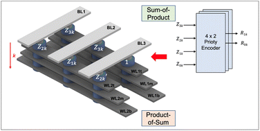
The self-rectifying memristor with electronic bipolar resistive switching shows electroforming-free, highly rectifying properties and low operating power. Furthermore, configuring the memristors in a vertical array structure provides a higher memory density than in a planar array structure. These combined advantages can be exploited in in-memory computing, which may provide a new and efficient stateful logic gate with high parallelism compared to the conventional stateful logic gates in the planar array structure. The different switching mechanism compared to the previous logic gates based on filamentary-type switching is explained and exploited to realize the AND and OR Boolean logic gates. Since the AND and OR logic functions are the basic operations of sum-of-product (SoP) and product-of-sum (PoS) expressions, any canonical expression for Boolean logic can be implemented in the vertical crossbar array (CBA). Accordingly, the composite logic gate, such as an exclusive OR operation, is demonstrated. In addition, the implementation of the memristive priority encoder is proposed using parallel logic gates. Although the switching speed should be improved in further work, a higher parallelism with a larger number of layers in the vertical array structure can mitigate the low operation speed issue.


Introduction

As the demand for data processing units is growing for data-centric applications, developing new logic gates beyond the von-Neumann architecture is essential. In-memory processing combining the dynamic random-access memory and graphic process unit is a typical example of the current trend toward this end.1 However, they still belong to the von-Neumann computing category, which does not eliminate the critical memory wall problem. In this regard, in-memory computing is a promising candidate for resolving the issue by minimizing or removing the data movement between the processing unit and memory.2 Furthermore, logic gates can be comprised of memristors, known as stateful logic gates, which are beneficial for implementing all Boolean logic gates in fewer devices by logic cascading since the same physical input and output format for a logic gate can be encoded as resistance states of a memristor.

The memristor is a two-terminal device that can change its resistance between the high-resistance state, off-state (Roff), and the low-resistance state, on-state (Ron), when applying voltage or passing a controlled amount of electrical charge.3 The use of the filament-type memristor has been mainly focused on in-memory computing due to its high switching speed and stability among diverse resistive switching mechanisms.4–6 This mechanism uses the formation and rupture of the conductive filament by the applied bias above the threshold voltage, namely the set voltage (Vset) for the transition from Roff to Ron and the reset voltage (Vreset) for the transition from Ron to Roff.[thin space (1/6-em)]7 The bias polarities of the Vset and Vreset are different for bipolar resistive switching, which can be utilized to form a stateful logic gate. Combining the memristors into an array structure can conditionally alter their resistances to correspond to the results of the logic operation upon applying the bias.8 The input of the logic gate can be encoded into the initial resistance of the memristors, and the output of the logic gate is encoded into the final resistance, which is a typical method in the stateful logic circuit.9

The first phase of stateful logic gate development realized all possible Boolean logic operations and logic cascading for complex gates.8,10–12 Then, improvements in latency and area cost of the logic gate have been recently studied.13,14 Despite many previous studies demonstrating promising improvement in the unit logic device, circuit configuration, and drive algorithm, practical demonstration at the array level is still challenging. As the operation speed of the stateful logic circuit is generally lower than that of complementary metal-oxide-semiconductor devices, parallel operation of many circuit units is essential. Therefore, demonstrating the stateful logic circuits at the array level, such as in the passive crossbar array (CBA), is vital. However, the passive CBA generally has a sneak-current issue. In particular, filament-based memristors have a relatively high current level, aggravating the sneak-current problem further.15,16 Therefore, recent developments in selection devices, such as a selector or transistor, have focused on suppressing the sneak current.17,18 However, it involves many preparation challenges since the drivable current level of the selection device must match the operation current level of the memristor. The high operation current level of filamentary type memristors renders meeting this condition challenging.

Consequently, much attention has been drawn to the development of self-rectifying memristors (SRMs), which are known as an interface type of electronic switching that have a high rectification ratio, low power consumption, and electroforming-free characteristics.19–22 These characteristics are beneficial for using the SRM as a logic gate. Nevertheless, logic gates based on the SRM have not been reported yet due to retention problems. Since the switching mechanism of the SRM is related to the trapping and de-trapping of electrons in the trap states, the trapped electrons can be escaped if the trap levels are too shallow, especially at elevated temperatures. This problem of the SRMs incurs data retention problems, which may render them less explored for logic applications. A recent work published by the authors23 resolves the retention problem by engineering deeper trap levels inside the switching layer of HfO2 with aluminum (Al) doping, resulting in sufficient data retention time to be used as a logic gate. In addition, engineering the high work function using platinum (Pt) as the top electrode provides the self-rectifying characteristic, suppressing the sneak current for the possible demonstration of logic operations in the CBA in this work.

Herein, SRMs using Pt/Ta2O5/Al-doped HfO2/TiN (PTA:HT) stacked materials are fabricated in a two-layered 2 × 2 vertical CBA configuration to implement stateful logic gates. Consequently, new parallel ASM-two-2AND and ASM-two-2OR gates within the anti-serial (AS) memristors have been experimentally realized, which have a higher parallelism in the vertical CBA than in the planar CBA. For better representation in this work, the references to logic gates follow the nomenclature rule used in the previous study,13 where “Structure-N-n Function” was used. The number of logic inputs and memristor cells is represented by N and n, respectively. The types of structures include PM, APM, SM, ASM, and M, denoting “parallel memristors”, “antiparallel memristors”, “series memristors”, “antiserial memristors”, and “single memristors”, respectively. If a series resistor is added, the letter “R” is added to the structure name. For example, the ASM-two-2AND logic gate denotes two (N = 2) anti-serial memristors that take two inputs to operate the AND logic operation. The proposed parallel logic gates can further be used to implement any other logic gates expressed in the sum-of-product (SoP) and product-of-sum (PoS). As an example, the XOR logic function has been demonstrated. Lastly, a method for parallel logic gates has been introduced for the priority encoder based on SRMs.

Results and discussion

Self-rectifying memristors in crossbar array structures

PTA:HT SRMs were fabricated for the logic gate implementation in a two-layered vertical 2 × 2 CBA structure with bit lines (BLs) and word lines (WLs). The detailed fabrication process is introduced in the Experimental section. Fig. 1(a) shows the schematic diagram of the vertical CBA, wherein the two TiN WLs (width/thickness = 100/0.035 μm) are stacked, separated by a 60 nm thick SiO2 layer. These WL structures are covered by a 10 nm thick Al-doped HfO2 layer, the switching layer, and a 5 nm thick Ta2O5 rectifying layer. Pt BLs (width/thickness = 100/0.05 μm) are formed in the orthogonal direction on top, and thus, the two intersecting side-wall areas, indicated by the red arrow in Fig. 1(a), constitute two SRMs that can be switched in the lateral direction between WL and BL. SiO2 layers in the longitudinal cross-section of BL2 separate the top and bottom memristors, D2t2 and D2b2. The individual connection to the top and bottom layers can be controlled by different contact-pad open etching times to WLs. As a result, the four WLs shown in Fig. 1(b) are identified according to different pad-open regions. Accordingly, eight memristor cells can be defined in the 2 × 2 vertical CBA structure. The corresponding WL and BL numbers indicate each memristor at the intersection. For example, the SRM at the intersection between WL2 on the top layer (WL2t) and BL2 is named D2t2. To switch the D2t2 memristor to the Ron state, the bias of Vset can be applied to BL2 while WL2t is grounded. Since SiO2 layers effectively block the current flow between WLs, resistive switching can occur at the intersection of WL2t and BL2. The cross-sectional field-emission transmission electron microscope (FE-TEM) image of D2t2 and D2b2 memristors is shown in Fig. 1(c), which reveals they are separated by the SiO2 isolating layers. Fig. 1(d) shows a higher magnification TEM image of the D2t2 memristor. The location of the Al-doping can be found in energy dispersive spectroscopy images from the FE-TEM shown in Fig. S1 in the ESI.
image file: d3nr00271c-f1.tif
Fig. 1 The vertical crossbar array structure consisting of self-rectifying memristors. (a) The schematic diagram of the 2 × 2 array structure and its longitudinal section of BL and (b) its optical top-view image. (c) Cross-sectional TEM images of D2t2 and (d) its higher magnification TEM image.

By biasing one of the BLs and connecting one of the WLs to the ground, the electrical characteristics of the SRM in the vertical CBA can be measured to examine the possibility of an SRM being used as a logic gate. Fig. 2(a) shows the relatively uniform device-to-device variation. With a read voltage of ±5.5 V, the Ron and Roff of the SRM are summarized in Fig. 2(b). It is worth noting that the resistance states of the SRM in different bias polarities are different due to the self-rectifying property. Thus, the resistance states in positive and negative polarities are distinguished with the sign symbol to the subscripted name, i.e., R+on and R−on. The cycle-to-cycle variation of D1t1 shown in Fig. 2(c) indicates that the two discrete states of R+on and R+off can be distinguished for more than 100 cycles. Due to the deeper trap levels induced by the Al-doping effect, the states can be retained for up to 102 seconds at 85 °C, as shown in Fig. 2(d). Although state drift in R+on is still observed in the Al-doped memristor, the logic operation can be demonstrated considering that the operations are at room temperature with the reference point of 250 GΩ. Consequently, the fabricated SRMs in a 2 × 2 vertical CBA structure represent possible candidates to be used as logic gates. Compared to the conductive filament-based memristors, a switching voltage of +6.5 V for an SRM is considerably higher, and requires a higher voltage interface circuit. Although the low current sensing issue must be resolved in the peripheral design to operate AC measurement, much less operating power can be achieved when considering the on-current order of nA. In contrast, a filament-based memristor has an on-current range from hundreds of μA to several mA. Also, the charge-trap type operation method of this PTA:HT SRM requires a relatively long switching time, which the parallel operation of the circuit structure can mitigate.


image file: d3nr00271c-f2.tif
Fig. 2 The electrical characteristic of memristors in the vertical CBA. (a) The current–voltage relationship representing a low cell-to-cell variation with a set voltage of +6.5 V and a reset voltage of −7.0 V. (b) Electrical properties of the memristor at a read voltage of ±5.5 V. (c) The cycle-to-cycle test between R+on and R+off and (d) the data retention at 85 °C.

The parallelism of logic gates is related to structural features. Here, in this study, two commonly known CBA structures with the same array size of m × n are considered, where m and n are the numbers of WLs and BLs, respectively. The first CBA structure is a stacked planar CBA structure, where each CBA layer has crossing WLs and BLs. Fig. 3(a) represents a planar 2 × 2 CBA with a three-layer stack (k = 3). Two parallel logic circuits can be obtained among the possible WL-wise or BL-wise configurations. When the positive bias is applied to WL1t while connecting WL2t to the ground, the configuration is defined as WL-wise configuration (WLC), and four logic gates of AS memristors can be specified, as shown in the left panel of Fig. 3(b). Similarly, the four logic gates of AS memristors can be defined in BL-wise configuration (BLC) in the planar CBA when the positive bias is applied to the BL1b while connecting BL2b to the ground, as shown in the right panel of Fig. 3(b). The logic gates of AS memristors can be further classified into two groups. When the first top memristor among the AS memristors is positioned in the forward direction to the applied bias, the logic gate is defined as the forward anti-serial (FAS) logic gate. If the memristor is positioned in the reversed direction, it is defined as the reversed anti-serial (RAS) logic gate. Accordingly, two FAS and two RAS logic gates can be defined in the WLC. When n increases, the number of parallel configurations increases linearly, as shown in the left panel of Fig. 3(c). Assuming the logic operation takes a unit of time, the number of parallel logic operations in WLC per unit of time (nop,WLC) can be defined as:

 
nop,WLC = nNFAS + nNRAS,(1)
where NFAS and NRAS are the numbers of FAS and RAS logic gates, respectively, in the primitive parallel configuration that can be used to define basis functions for logic cascading. Similarly, the number of parallel logic operations in the BLC per unit of time (nop,BLC) can be defined for the given m, as shown in the right panel of Fig. 3(c):
 
nop,BLC = mNFAS + mNRAS(2)


image file: d3nr00271c-f3.tif
Fig. 3 The planar 2 × 2 crossbar array structure. (a) The three-layered structure and its configurations. The equivalent circuit of configurations when (b) n = 2, m = 2, and k = 3, and (c) for a larger size. The red and blue dotted boxes represent RAS and FAS logic gates, respectively. The number of possible circuits is independent of k.

The parallelism of logic gates can be improved by increasing the planar CBA size with m or n but is independent of k when k ≥ 3 in the planar CBA structure. In this case, increasing the k value does not enhance parallelism, which can be understood from the fundamental two-dimensional arrangements of the WLs and BLs in this structure. On the other hand, the parallelism of logic gates in the suggested vertical CBA can further be improved by increasing k. The schematic diagram of a three-layered 2 × 2 vertical CBA is shown in Fig. 4(a). On applying the bias to WL1t and connecting WL2t to the ground, the equivalent circuit obtained is presented in the left panel of Fig. 4(b). In the vertical CBA, only RAS logic gates can be realized in WLC. When n increases, nop,WLC is given by the following equation, as shown in the left panel of Fig. 4(c):

 
nop,WLC = nNRAS(3)


image file: d3nr00271c-f4.tif
Fig. 4 The vertical 2 × 2 crossbar array structure. (a) The three-layered structure and its configurations. The equivalent circuit of configurations when (b) n = 2, m = 2, and k = 3, and (c) for a larger size. The high parallel FAS gates indicated in blue dotted boxes can be achieved in the BLC. The number of possible circuits in the BLC is dependent on k.

Compared to the planar CBA, the number of parallel operations in RAS logic gates is the same, but the FAS logic gate is not implemented in WLC. Instead, the FAS logic gates are implemented in the BLC, as shown in the right panel of Fig. 4b. The parallelism can be further improved by increasing m, similar to that in the right panel of Fig. 3c. Still, the k-times more parallel FAS logic gates can be implemented in the BLC in this case, as shown in the right panel of Fig. 4c, given by the following equation:

 
nop,BLC = kmNFAS(4)

Thus, the number of parallel operations in FAS logic gates can be the application, and simultaneous operations of FAS and RAS logic gates may be required. However, operating one type of logic gate at a time provides much higher parallelism and efficiency in general applications. Therefore, the following sections explain the details of the parallel operation of the logic gates using vertical CBA devices.

Parallel logic gates in a vertical crossbar array structure

The FAS and RAS logic gates can be implemented in the two-layered vertical CBA structure for the BLC and WLC. For simplicity, the bias configuration between two nodes is expressed as the 〈applied bias node (applied voltage), ground node (0)〉. For example, when the bias of Va is applied to BL1 and BL2 is connected to ground, the simplified expression is 〈BL1 (Va), BL2 (0)〉. To define the two-input logic gates in the BLC, the Roff and Ron states are encoded as logical “0” and “1”, respectively. The memristors are initialized to “0” states at the initial stage. Then, the two input bits, p and q, of the FAS logic gate are stored in D1t1 and D1t2 memristors, respectively, as their resistance values. Then, 〈BL1 (Va,AND), BL2 (0)〉 can be applied to realize the ASM-two-2AND gate, as shown in Fig. 5(a), where Va,AND = +9 V. Among the possible FAS logic gates shown in Fig. 4(c), the AND gating operation of the AS memristors with D1t1 and D1t2 is shown for simplicity in this figure.
image file: d3nr00271c-f5.tif
Fig. 5 Experimental demonstration of the AND logic gate between D1t1 and D1t2 memristors in the BLC. (a) The bias configuration in the schematic diagram of the vertical CBA, where Va,AND = +9 V. (b) The results of the AND logic operation in D1t1 for each input case. A resistance lower than 250 GΩ is encoded to the “1” state and (c) its truth table of the logic gate.

The results of the other parallel FAS logic gates in the BLC are included in Fig. S2 in the ESI. Since two input bits have four possible input cases, the resistance values of the two memristors at a reading voltage of +5.5 V for each case are shown in Fig. 5(b). The apostrophe to the name represents the memristors in the final state after the logic operation. The logic operation results can be summarized in the truth table, shown in Fig. 5(c). The resistance values of D′1t1 represent the output bit of the two-input AND logic operation (r′). It is worth noting that inputs of the proposed ASM-two-2AND gate are destructive, and the unselected memristor, D1t2, is concurrently reinitialized to the “0” state after the logic operation, which is related to the de-trapping of electrons in the unselected memristor. Since the conduction mechanism of the SRM involves the trapping and de-trapping of electrons in trap states,24 the unselected memristor donates electrons to the selected memristor, resulting in a “0” state. Such reinitialization is advantageous for sequential data processing within the confined memory space. By removing the additional separate initialization step to the input memristors for the next logic operation, efficient parallel logic operations can be achieved. Similarly, the ASM-two-2OR gates can be defined in the WLC.

The two input bits, p and q, are programmed to D1t1 and D2t1, as shown in Fig. 6(a). When the bias configuration of 〈WL1t (Va,OR), WL2t (0)〉 is used, where Va,OR = +12 V, the resultant output bit of the ASM-two-2OR gate is stored to the D2t1 memristor (D′2t1). The resistance states of D1t1 and D2t1 at the initial and final states are shown in Fig. 6(b). Thus, the selected memristor represents the two-input OR function, as shown in the truth table in Fig. 6(c), and the unselected memristor (D′1t1) is reinitialized to the “0” state after the logic operation. The different logic functions can be achieved by modulating the location of the Schottky barrier in the band structure. However, the sneak current in the vertical CBA must be negligible to implement the above-mentioned logic gate operations into the SRM-based circuit. The sneak current can be suppressed by the appropriate bias scheme, such as a 1/2 or 1/3 voltage scheme for the selected and unselected memristor. However, biasing the selected and unselected WLs and BLs costs hardware complexity and high energy consumption.25 Instead, a floating scheme can be applied with the self-rectifying memristor with a relatively high rectification ratio, suppressing the reverse path of the sneak current. This condition was verified in the logic operations of the ASM-two-2AND gate by placing memristor states in the worst case that promotes the sneak-current path, as shown in Fig. S3 in the ESI. As a result, the sneak current was efficiently suppressed in the 2 × 2 vertical CBA so that it could be neglected throughout the study. When the bias is applied to logic gates, i.e., ASM-two-2AND gates between D1t1 and D1t2, the voltage drop by the SRM is determined by the voltage divider between two memristors having four possible states of R−on, R−off, R+on, and R+off. The following equation provides the voltage drop over D1t2:

 
image file: d3nr00271c-t1.tif(5)


image file: d3nr00271c-f6.tif
Fig. 6 Experimental demonstration of the OR logic gate between D1t1 and D1t2 memristors in WLC. (a) The bias configuration in the schematic diagram of the vertical CBA, where Va,OR = +12 V. (b) The results of the logic operation are stored in the D2t1 for each input case. (c) The truth table of the logic gate.

R D1t1 and RD1t2 are the resistances of D1t1 and D1t2 memristors, respectively. When the voltage drop over D1t2 is larger than the magnitude of Vreset, the resistance of the memristor is switched to Roff. When filament-based memristors are used, such switching of each memristor does not influence the switching behavior of nearby memristors as long as the sneak current is sufficiently suppressed. However, this independent switching may not be the case, but additional adverse switching occurs in the PTA:HT device.20,23,26,27

Since the reset process of the electronic bipolar resistive switching memristors is the de-trapping of electrons from the trap states, the de-trapped electrons can fill the trap states in the adjacent memristor, connected to the switching memristor via metal wires. Fig. 7 shows the energy band diagrams at the applied bias for ASM-two-2AND and ASM-two-2OR gates based on the parameters given in Tables S4-1 and S4-2 in the ESI. The static dielectric constants of the Al-doped HfO2 and Ta2O5 are reported to be ≈21 and ≈26, respectively.28,29 Thus, the electric field across the Al-doped HfO2 is higher than that across the Ta2O5 layer, making the switching layer Al-doped HfO2. In the Poole–Frenkel fitting in the previous work,20 the trap level is 1.69 eV, which has higher trap energy levels than the undoped HfO2 layer, outlined with the red dashed line in the energy band diagram.


image file: d3nr00271c-f7.tif
Fig. 7 Energy band diagram of AND and OR logic gates. (a) The ASM-two-2AND gate between D1t1 and D1t2 memristors and (b) ASM-two-2OR gate between D1t1 and D2t1 for each input case when a bias of +9 V and +12 V is applied for the logic operation, respectively.

When the memristor is initialized to R±on states, all deep trap levels are assumed to be filled, whereas trap levels in R±off states are considered empty. The rate of the transportation depends on the slope of the band tilting, which is governed by the built-in potential and applied bias to the memristor given by the voltage divider in eqn (5). For instance, the internal potential of the oxides, ϕi, is 1.13 eV, which corresponds to the difference between the work functions of Pt and TiN (5.65 eV–4.52 eV).30,31 The resultant band tilting of the forward memristor in the ASM-two-2AND logic gate would be qVD1t1ϕi and of the reversed memristor it is qVD1t2 + ϕi. When the bias of Va,AND is applied to the ASM-two-2AND gate, as shown in Fig. 7(a), the carrier injection from the Pt electrode to the Ta2O5 layer is effectively prevented due to the high Schottky barrier height, and only transport of the trapped electrons from D1t2 to D1t1 is allowed during the logic operation. In the input case I, no transportation of electrons occurs during the logic operation because the traps in both D1t1 and D1t2 are empty. Accordingly, the final states of the memristors are the same as the initial states. On the other hand, the trap states in D1t2 are filled with electrons in input case II. Thus, RD1t2 is decreased to R−on from R−off. Consequently, the slope of the band tilting in D1t1 is higher than that of the band tilting in D1t2, which results in a faster de-trapping rate in D1t1. In other words, the de-trapped electrons in D1t2 can fill the trap states in D1t1, but the faster de-trapping rate in D1t1 results in the empty states. In input case III, the band tilting in D1t1 is smaller than the band tilting in D1t2, which means trapping the electrons in D1t1 by the de-trapped electrons from D1t2 would be faster. However, the final trap states in D1t1 are empty since the trap states in D1t2 were empty. In contrast, the trap states in D1t2 are filled with electrons in input case IV. Thus, the resultant trap states in D1t1 are now filled with electrons, resulting in the ASM-two-2AND gate operation.

Similarly, the ASM-two-2OR logic gate can be interpreted with the same model based on the energy band diagram. For instance, Fig. 7(b) shows the energy band diagram when the applied bias of Va,OR is applied to the ASM-two-2OR logic gate between D1t1 and D2t1. The resultant applied voltages of the forward and reverse memristors in the ASM-two-2OR logic gate are qVD2t1ϕi and qVD1t1 + ϕi, respectively. The Schottky barrier is now related to the Pt electrode, located between D1t1 and D2t1. Then, the carrier transport between D1t1 and D2t1 is prohibited, which means that only the de-trapping electrons in D1t1 to the TiN electrode or trapping electrons to D2t1 from the Pt electrode is possible. In input case I, the injected electrons can fill the trap states in D2t1, but the voltage drop over D2t1 is insufficient because a higher voltage drop occurs over D1t1. In input case II, the trap states in D2t1 are filled with electrons. Since the de-trapping electrons in D2t1 are not allowed due to the Schottky barrier, the trapped electrons remain intact after the logic operation. In input case III, the trap states in D1t1 are now filled with electrons, reducing RD1t1 to R+on from R+off. Therefore, the voltage drops over D2t1 are higher than the voltage drops in input case I, resulting in the possible injection of electrons into D2t1. Lastly, the filled trap states in D2t1 in input case IV remain intact due to the Schottky barrier. For the above reasons, the final states of D2t1 represent the ASM-two-2OR gate. Such an interpretation does not consider the space charge nor defects in the fabrication for simplicity, and this will be considered in future work.

Logic cascading in a vertical array structure and its application

The ASM-two-2AND and ASM-two-2OR gates can be further implemented in other Boolean logic operations. Since PoS and SoP are based on the AND and OR functions, functional completeness can be achieved using two parallel logic gates with NOT initialization. For instance, the XOR logic function between two input bits (FXOR_pq) can be completed in two steps after the initialization. The XOR function can be expressed in the following equation:
 
FXOR\_pq = (p + q)([p with combining macron] + [q with combining macron]) = [p with combining macron]q + p[q with combining macron].(6)

Therefore, the PoS form of the XOR function can be implemented with two ASM-two-2OR gates and one ASM-two-2AND gate, whereas the SoP form of the XOR function requires two ASM-two-2AND gates and one ASM-two-2OR gate. Since the vertical CBA has higher parallelism in AND gates, the SoP form of the XOR function is used for the demonstration. Fig. 8(a) shows the 2 × 2 vertical CBA structure for ASM-two-2AND and ASM-two-2OR gates. The numbers in the box represent the step number, and the bold arrows indicate the data result flow after logic operations between two AS memristors. The demonstration implies that two logic operations, either in WLC or BLC, can be combined and stored to the target memristor, i.e., D1t1. First, ASM-two-2AND gates are operated with the bias configuration of 〈VBL1 (Va,AND), VBL2 (0)〉. Then, the results of two ASM-two-2AND gates are stored in D1t1 and D2t1 memristors, and other memristors are reinitialized to the “0” state. Second, the final cascaded result of the XOR function can be obtained in D1t1 by operating ASM-two-2OR gates with the bias configuration of 〈VWL1t (Va,OR), VWL2t (0)〉. Fig. 8(b) shows the computational procedure and memristor states at each step. Since the unselected memristors assume a “0” state after the logic operation, the reinitialization cost for the following logic operation can be reduced. Fig. 8(c) shows the XOR gating process. The normalized resistance for 250 GΩ is used to distinguish the states, where the bright color corresponds to the R+on state. Compared to single-cycle logic gates,32,33 parallel logic gates have an advantage in the application where multiple bits are involved. For instance, the 4 × 2 priority encoder takes four input bits, Z0k, Z1k, Z2k, and Z3k, and gives two output bits, R0k and R1k, and its truth table is shown in Fig. 9(a). The following equations define the outputs:

 
image file: d3nr00271c-t2.tif(7)
 
R1k = Z3k + Z2k(8)


image file: d3nr00271c-f8.tif
Fig. 8 Realization of the XOR function using cascading of parallel logic gates in the 2 × 2 vertical CBA. (a) Bias scheme in ASM-two-2AND and ASM-two-2OR gates. (b) The computation procedure. (c) Experimental demonstration for each input case.

image file: d3nr00271c-f9.tif
Fig. 9 Implementation of 4 × 2 priority encoders in the three-layered 2 × 3 vertical CBA. (a) The truth table of a priority encoder, where “X” bit represents the “don't care” term. (b) The schematic diagram of k-layered priority encoders. (c) The computational procedure.

When non-parallel stateful logic gates are used, they require one step for the AND gate and two steps for OR gates to implement the 4 × 2 priority encoder. In contrast, the parallel logic gates of ASM-two-2AND and ASM-two-2OR require one step for the AND gate and one step for the OR gate. The “X” in the truth table represents the “don't care” term in which either “1” or “0” can be replaced.

The difference becomes more significant when multiple encoders are required, as shown in Fig. 9(b). For the three 4 × 2 priority encoders, non-parallel stateful logic gates would require three steps for the AND gate and six for the OR gate, neglecting the data transfer operations. In contrast, the parallel logic gates can operate the encoders in the same steps as one 4 × 2 priority encoder if k is greater or equal to the number of the required encoders. First, the memristors are initialized, as shown in Fig. 9(c). Here, the subscripted letter “k” corresponds to the number of layers. For instance, the D1t1 memristor located at the first layer (k = 1) is initialized to Z31. After the initialization, the operation of parallel ASM-two-2AND gates is conducted with the bias configuration of 〈BL3 (Va,AND), BL2 (0)〉. The results of the eight memristors are presented in the computation scheme. Then, the parallel ASM-two-2OR gates with the bias configuration of 〈WL1t (Va,OR), WL2t (0)〉 result in a 4 × 2 priority encoder, where each layer represents the kth encoder. Although logic implementation in vertical CBA requires further exploration, the electroforming-free and high rectification ratio of SRM with the high parallelism in vertical CBA are highly promising in in-memory computing.

Experimental sections

Device fabrication

The bottom electrode of 35 nm thick TiN was deposited on a SiO2/Si substrate using radio frequency (RF) sputtering (Sorona, SRN 120). Next, the 60 nm thick SiO2 layer was deposited using plasma-enhanced chemical vapor deposition (PECVD) equipment (Oxford instrument, PlasmaPro System100). Then, the deposition of 35 nm thick TiN was repeated for the top layer of the vertical structure. The passivation layer of 30 nm thick SiO2 was deposited using PECVD to prevent oxidation. Photoresist (SS03A9) was patterned using maskless lithography (Nano System Solutions. Inc, DL-1000HP), and the sample was dry-etched using an ICP etcher (Gigalane, NeoS-MAXIS 200L) for the bottom patterning. The byproduct of the etching was removed utilizing a plasma asher (Plasma finish, V15-G). Finally, 60 nm thick SiO2 was deposited using PECVD to prevent parasitic resistive switching. The vertical hole structure was also created using an ICP etcher and asher after the hole photoresist pattern was created by photolithography. The hole structure was filled with a resistive switching layer of 10 nm thick Al-doped HfO2 using 100 cycles of atomic layer deposition (ALD, CN-1, custom-made ALD cluster system). For every tenth cycle, 9 cycles of the HfO2 film were deposited using Hf[N(CH3)2]4 and O3 as the Hf precursor and the oxygen source, respectively, followed by the 1 cycle of Al layers using the Al(CH3)3 precursor. Next, the rectifier layer of Ta2O5 film was deposited with another ALD (CN-1, Atomic Premium plus 200) using (CH3)3CNTa[N(C2H5)2]3 and H2O-activated plasma as the Ta precursor and the oxygen source, respectively. Next, a 50 nm thick Pt top electrode was deposited using an electron beam evaporator (SORONA, SRN-200i), followed by the lift-off process. The pad-open process involved the following steps. The resistive switching layers were removed using an ICP etcher (Oxford Instruments, PlasmaPro System 100 Cobra) until reaching the passivation layer of SiO2. Then, the passivation layer was removed by a wet etching process using buffered oxide etchant (BOE) until the TiN top layer was opened. The TiN layer was removed using the ICP etcher using Cl2 and BCl3 gases. The BOE removed the SiO2 layers to open the top and bottom layers of the bottom electrodes. Details of the device fabrication are reported elsewhere.23

Electrical characterization

The cross-section of the Pt/Ta2O5/Al-HfO2/TiN sample was observed using a high-resolution TEM (JEOL, JEM-F200) with an accelerating voltage of 200 kV and field-emission scanning electron microscope (Hitachi, S4800). The electrical measurements were conducted using an HP4145B semiconductor parameter analyzer.

Conclusions

Logic gates based on aluminum-doped self-rectifying memristors have advantages of being electroforming-free, having sufficient data retention time, and preventing the sneak-current from high rectification in a crossbar array structure. Still, the slow logic operation speed of the stateful logic gates emphasizes the importance of parallelism. In this study, the vertical crossbar array structure reveals that higher parallelism can be achieved in logic gates based on memristors, which have a higher number of logic operations in a word-line configuration than in the planar structure. For demonstration, aluminum-doped HfO2-based self-rectifying memristors are fabricated in a vertical 2 × 2 crossbar array. Two Boolean logic gates of AND and OR are demonstrated in word-line- and bit-line-wise configurations and interpreted using the energy band diagram model. The logic synthesis method of using the logic cascading of the proposed logic gates is explained with the product-of-sum and sum-of-product forms. Then, the demonstration of the XOR function using the product-of-sum is represented. Lastly, the efficiency of parallel logic gates is emphasized with the implementation of three layers of 4 × 2 priority encoders. Although the proposed logic gate should be further elaborated on a larger scale of the vertical array structure, considering the parasitic capacitance and line resistance, this work introduces a promising logic implementation in the vertical CBA using self-rectifying memristors.

Author contributions

T. Park conceived the idea, arranged figures, and wrote the manuscript, and S. S. Kim fabricated the memristors and measured the logic operations. B. J. Lee participated in band diagram drawing. T. W. Park assisted with reference works. H. J. Kim and C. S. Hwang supervised the whole research and manuscript preparation.

Conflicts of interest

There are no conflicts to declare.

Acknowledgements

T. Park and S. S. Kim contributed equally to this work. This work was supported by the National Research Foundation of Korea (2021R1A3B2079882).

References

  1. Y.-C. Kwon, S. H. Lee, J. Lee, S.-H. Kwon, J. M. Ryu, J.-P. Son, S. O, H.-S. Yu, H. Lee, S. Y. Kim, Y. Cho, J. G. Kim, J. Choi, H.-S. Shin, J. Kim, B. Phuah, H. Kim, M. J. Song, A. Choi, D. Kim, S. Kim, E.-B. Kim, D. Wang, S. Kang, Y. Ro, S. Seo, J. Song, J. Youn, K. Sohn and N. S. Kim, in 2021 IEEE International Solid- State Circuits Conference (ISSCC), 2021, pp. 350–352.
  2. A. Sebastian, M. le Gallo, R. Khaddam-Aljameh and E. Eleftheriou, Nat. Nanotechnol., 2020, 15, 529–544 CrossRef CAS PubMed.
  3. R. Waser, R. Dittmann, C. Staikov and K. Szot, Adv. Mater., 2009, 21, 2632–2663 CrossRef CAS PubMed.
  4. B. J. Choi, A. C. Torrezan, J. P. Strachan, P. G. Kotula, A. J. Lohn, M. J. Marinella, Z. Li, R. S. Williams and J. J. Yang, Adv. Funct. Mater., 2016, 26, 5290–5296 CrossRef CAS.
  5. M. J. Lee, C. B. Lee, D. Lee, S. R. Lee, M. Chang, J. H. Hur, Y. B. Kim, C. J. Kim, D. H. Seo, S. Seo, U. I. Chung, I. K. Yoo and K. Kim, Nat. Mater., 2011, 10, 625–630 CrossRef CAS PubMed.
  6. N. Xu, T. Park, K. J. Yoon and C. S. Hwang, Phys. Status Solidi RRL, 2021, 15 Search PubMed.
  7. D. H. Kwon, K. M. Kim, J. H. Jang, J. M. Jeon, M. H. Lee, G. H. Kim, X. S. Li, G. S. Park, B. Lee, S. Han, M. Kim and C. S. Hwang, Nat. Nanotechnol., 2010, 5, 148–153 CrossRef CAS PubMed.
  8. J. Borghetti, G. S. Snider, P. J. Kuekes, J. J. Yang, D. R. Stewart and R. S. Williams, Nature, 2010, 464, 873–876 CrossRef CAS PubMed.
  9. D. Ielmini and H. S. P. Wong, Nat. Electron., 2018, 1, 333–343 CrossRef.
  10. N. Xu, T. G. Park, H. J. Kim, X. Shao, K. J. Yoon, T. H. Park, L. Fang, K. M. Kim and C. S. Hwang, Adv. Intell. Syst., 2020, 2, 1900082 CrossRef.
  11. K. M. Kim and R. Stanley Williams, IEEE Trans. Circuits Syst. I Regul. Pap., 2019, 66, 4348–4355 Search PubMed.
  12. J. Shen, P. Lu, D. Shang and Y. Sun, Phys. Rev. Appl., 2019, 12, 054062 CrossRef CAS.
  13. N. Xu, T. Park, K. J. Yoon and C. S. Hwang, Phys. Status Solidi RRL, 2021, 15 Search PubMed.
  14. Y. S. Kim, M. W. Son and K. M. Kim, Adv. Intell. Syst., 2021, 3, 2000278 CrossRef.
  15. H. Y. Lee, P. S. Chen, T. Y. Wu, Y. S. Chen, C. C. Wang, P. J. Tzeng, C. H. Lin, F. Chen, C. H. Lien and M. J. Tsai, in Technical Digest - International Electron Devices Meeting, IEDM, 2008.
  16. K. M. Kim, G. H. Kim, S. J. Song, J. Y. Seok, M. H. Lee, J. H. Yoon and C. S. Hwang, Nanotechnology, 2010, 21, 305203 CrossRef PubMed.
  17. V. A. Demin, I. A. Surazhevsky, A. V. Emelyanov, P. K. Kashkarov and M. V. Kovalchuk, J. Comput. Electron., 2020, 19, 565–575 CrossRef CAS.
  18. X. Peng, R. Madler, P. Y. Chen and S. Yu, J. Comput. Electron., 2017, 16, 1167–1174 CrossRef CAS.
  19. D. E. Kwon, J. Kim, Y. J. Kwon, K. S. Woo, J. H. Yoon and C. S. Hwang, Phys. Status Solidi RRL, 2020, 14, 2000209 CrossRef CAS.
  20. J. H. Yoon, S. J. Song, I. H. Yoo, J. Y. Seok, K. J. Yoon, D. E. Kwon, T. H. Park and C. S. Hwang, Adv. Funct. Mater., 2014, 24, 5086–5095 CrossRef CAS.
  21. Y. Kim, J. Kim, S. S. Kim, Y. J. Kwon, G. S. Kim, J. W. Jeon, D. E. Kwon, J. H. Yoon and C. S. Hwang, Adv. Intell. Syst., 2020, 2, 1900116 CrossRef.
  22. Z. Chen, R. Song, Q. Huo, Q. Ren, C. Zhang, L. Li and F. Zhang, Micromachines, 2021, 12, 614 CrossRef PubMed.
  23. S. S. Kim, S. K. Yong, J. Kim, J. M. Choi, T. W. Park, H. Y. Kim, H. J. Kim and C. S. Hwang, Adv. Electron. Mater., 2022, 2200998 Search PubMed.
  24. J. H. Yoon, S. J. Song, I. H. Yoo, J. Y. Seok, K. J. Yoon, D. E. Kwon, T. H. Park and C. S. Hwang, Adv. Funct. Mater., 2014, 24, 5086–5095 CrossRef CAS.
  25. K. J. Yoon, W. Bae, D. K. Jeong and C. S. Hwang, Adv. Electron. Mater., 2016, 2, 1600326 CrossRef.
  26. K. Jeon, J. Kim, J. J. Ryu, S. J. Yoo, C. Song, M. K. Yang, D. S. Jeong and G. H. Kim, Nat. Commun., 2021, 12, 2968 CrossRef CAS PubMed.
  27. K. Jeon, J. J. Ryu, D. S. Jeong and G. H. Kim, Adv. Mater. Interfaces, 2022, 9, 2200392 CrossRef CAS.
  28. M. M. Rahman, J. G. Kim, D. H. Kim and T. W. Kim, Micromachines, 2019, 10, 361 CrossRef PubMed.
  29. B. Renner, P. Lunkenheimer, M. Schetter, A. Loidl, A. Reller and S. G. Ebbinghaus, J. Appl. Phys., 2004, 96, 4400–4404 CrossRef CAS.
  30. D. Gu, S. K. Dey and P. Majhi, Appl. Phys. Lett., 2006, 89, 082907 CrossRef.
  31. C. Y. Wang, C. Y. Chou, H. F. Shiue, H. Y. Chen, C. H. Ling, J. J. Shyue and M. J. Chen, Appl. Surf. Sci., 2022, 585, 152748 CrossRef CAS.
  32. N. Taherinejad, IEEE Trans. Very Large Scale Integr. VLSI Syst., 2021, 29, 925–935 Search PubMed.
  33. T. Park, Y. R. Kim, J. Kim, J. Lee and C. S. Hwang, Adv. Intell. Syst., 2022, 4, 2100267 CrossRef.

Footnote

Electronic supplementary information (ESI) available: EDS analysis, parallel operations, and model. See DOI: https://doi.org/10.1039/d3nr00271c

This journal is © The Royal Society of Chemistry 2023