
 Open Access Article
 This Open Access Article is licensed under a Creative Commons Attribution-Non Commercial 3.0 Unported Licence
Nanoscale friction on MoS2/graphene heterostructures†
Zhao
Liu‡
 a,
Bartosz
Szczefanowicz
a,
J. Marcelo J.
Lopes
b,
Ziyang
Gan
c,
Antony
George
c,
Andrey
Turchanin
c and
Roland
Bennewitz
*a
a,
Bartosz
Szczefanowicz
a,
J. Marcelo J.
Lopes
b,
Ziyang
Gan
c,
Antony
George
c,
Andrey
Turchanin
c and
Roland
Bennewitz
*a
aINM – Leibniz Institute for New Materials, Campus D22, 66123 Saarbrücken, Germany. E-mail: roland.bennewitz@leibniz-inm.de
bPaul-Drude-Institute für Festkörperelektronik, Leibniz-Institut im Forschungsverbund Berlin e.V., Hausvogteiplaz 5-7, 10117 Berlin, Germany
cFriedrich Schiller University Jena, Institute of Physical Chemistry, Lessingstr. 10, 07743 Jena, Germany
First published on 27th February 2023
Abstract
Stacked hetero-structures of two-dimensional materials allow for a design of interactions with corresponding electronic and mechanical properties. We report structure, work function, and frictional properties of 1 to 4 layers of MoS2 grown by chemical vapor deposition on epitaxial graphene on SiC(0001). Experiments were performed by atomic force microscopy in ultra-high vacuum. Friction is dominated by adhesion which is mediated by a deformation of the layers to adapt the shape of the tip apex. Friction decreases with increasing number of MoS2 layers as the bending rigidity leads to less deformation. The dependence of friction on applied load and bias voltage can be attributed to variations in the atomic potential corrugation of the interface, which is enhanced by both load and applied bias. Minimal friction is obtained when work function differences are compensated.
Van der Waals heterostructures are stacks of 2D materials which are held together by the van der Waals attraction among the molecular sheets. Their specific assembly allows for a tuning of materials properties.1 Misfit strain, charge redistribution, and interlayer coupling affect electronic and plasmonic structure of the heterostructures and open new opportunities for electronic and optical devices.2 One example of mechanical mechanisms in van der Waals heterostructures is the demonstration of self-reorientation in the graphene/h-BN system.3 The high in-plane strength and weak out-of-plane interaction of 2D materials have brought them into the focus of tribology, the science of friction, wear, and lubrication. Especially graphene and MoS2, the building blocks of well-established solid lubricants, have been investigated with respect to mechanisms of lubrication.4–9
Friction on van der Waals heterostructures is studied in two categories. In the first category, the shear plane lies between the 2D materials forming the heterostructure. Examples are the pioneering work by Dienwiebel et al. on structural lubricity as function of the twist angle between graphene attached to the tip and graphene as top layer of graphite,5 the demonstration of the same effect for MoS2,9 and the recent study on edge- and step-pinning effects for MoS2 sliding on graphitic surfaces.10 Important concepts in this category are structural superlubricity11 and the role of charge redistribution for the effective potential surface of sliding 2D materials.12 Structural lubricity within heterostructures was demonstrated not only in nanoscale but also in micrometer-scale systems.13
In the second category, sliding friction is measured and modeled for contacts on top of heterostructures of 2D materials. For example, Lavini et al. have discovered an odd–even contrast for the number of MoS2 layers on graphene14 and Vazirisereshk et al. have quantified the friction contrast between each 2D material and the MoS2/graphene heterostructure.15 The interaction of mismatched lattices in graphene/h-BN has been revealed as Moiré pattern in atomic-scale friction maps recorded on the heterostructure.16,17
The combination of attractive tribological and exotic electronic properties has motivated studies on the control of friction on 2D materials by applying an electrical field across the sliding contact. A dependence of nanoscale friction on the applied tip–sample bias has been reported for graphene,18,19 h-BN,20,21 MoS2,22,23 and MoSe2.24 The enhancement of adhesion by electrostatic attraction was identified as a major contribution to friction. All these studies were carried out in ambient environment and effects of the electric field on capillary water bridges at the contact were investigated for their role in friction enhancement.19,20
Here, we report results for nanometer-scale friction on 1–4 layers of chemical vapor deposition (CVD) grown MoS2![[thin space (1/6-em)]](https://www.rsc.org/images/entities/char_2009.gif) 25,26 on epitaxial graphene on SiC(0001).27 Friction force microscopy experiments were performed in ultra-high vacuum using both conductive and insulating probes to investigate the effects of an applied bias voltage. Relevant parameters of adhesion and friction as function of the applied bias voltage are discussed in terms of contact mechanics for the bendable 2D materials, electrostatic adhesion, and polarization of the MoS2.
25,26 on epitaxial graphene on SiC(0001).27 Friction force microscopy experiments were performed in ultra-high vacuum using both conductive and insulating probes to investigate the effects of an applied bias voltage. Relevant parameters of adhesion and friction as function of the applied bias voltage are discussed in terms of contact mechanics for the bendable 2D materials, electrostatic adhesion, and polarization of the MoS2.
1. Results
The CVD growth of MoS2 on graphene/SiC(0001) resulted in a distribution of islands of varying height, ranging from single layers to four or more layers. A typical triangular monolayer MoS2 island is shown in Fig. 1a. The measured height of the island is 0.5 nm, a little less than expected based on chemical structure and reported previously.15,28 The simultaneously recorded friction force map shows higher friction on the MoS2 island compared to the graphene/SiC(0001) substrate. Throughout this report, friction is recorded for the oxidized silicon tip of the AFM sliding on stationary MoS2 islands. In contact mode, the AFM tip can displace MoS2 islands on atomically flat graphene terraces even at very low applied forces.29,30 Here we report results only for islands which are firmly attached to substrate features such as steps of the SiC(0001) substrate. No tip-induced shear displacement of MoS2 layers with respect to the underlying MoS2 island was observed in our friction experiments. Friction maps with atomic stick-slip pattern (see ESI†) reveal that the MoS2 islands are aligned with graphene substrate lattice. The Moiré pattern of the complex interface between reconstructed SiC(0001) and graphene (see ref. 6) obscures any Moiré pattern on monolayer MoS2, which could be expected from the lattice mismatch between graphene and MoS2.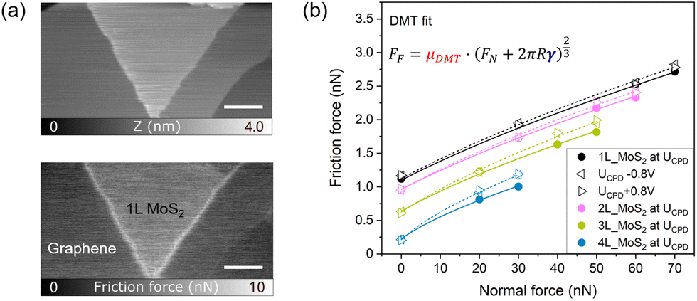 | ||
| Fig. 1 (a) Topographic contact-mode AFM image of a monolayer triangular MoS2 island grown on monolayer graphene/SiC(0001), and friction force map recorded simultaneously with the data presented in (a) at a load of 2.73 nN (scale bars: 100 nm). (b) Friction force as a function of normal force for 1–4 layers of MoS2 on graphene/SiC(0001). Results are presented at compensated contact potential difference (●) and 0.8 V above (▷) or below (◁) using a conductive tip. The data are fitted with the DMT model indicated. | ||
The load dependence of friction on MoS2 islands with a thickness between 1 and 4 layers is summarized in Fig. 1b. The load dependence exhibits the sub-linear characteristic of single-asperity friction with significant adhesion.15,31 Friction decreases from 1 to 4 layers of MoS2, primarily due to a decrease in adhesion. Fig. 1b also shows the relatively small changes in friction when a bias voltage is applied to the sample. We have determined the contact potential difference (CPD) between tip and sample as the bias voltage UCPD at which the electrostatic tip–sample attraction is minimized. This measurement is performed in non-contact mode by Kelvin Probe Force Microscopy (KPFM).32 Friction data was recorded at compensated contact potential difference and for selected voltages above and below UCPD.
To describe the dependence of the friction force FF on the normal force FN by relevant parameters, we have modeled it as FF = τ·A, where τ is the shear strength and A is the contact area which is described by the Derjaguin–Muller–Toporov (DMT) contact mechanics model:33
 | (1) |
 . The DMT fits describe the non-linear load dependence of friction by two parameters, the tip-specific friction coefficient μDMT for single-asperity friction and the adhesion energy γ, which is defined by an adhesive contribution to friction at zero applied load. We will discuss below in how far the deformation of layered materials limits the applicability of the DMT contact mechanics model.34
All experimental results presented in Fig. 1 were recorded with one electrically conductive AFM tip. The conductivity of each tip depends on the thickness of the oxide layer at the tip apex, which is easily worn off in contact-mode experiments. Since we have found differences in bias-dependent friction between conductive and insulating tips, we characterize their properties in comparison. The electrical current vs. applied voltage for a conductive tip in contact with 1 to 4 layers of MoS2 is plotted in Fig. 2a. The current depends strongly on the applied normal load, increasing from 20 to 370 pA when increasing the normal load from 0 nN to 70 nN on a monolayer MoS2 at a bias of −1.2 V. On 4 layers of MoS2, the current increases only from 6 to 12 pA in the same range of normal forces. While we cannot offer a predictive model for the current–voltage characteristics of the interface comprising doped silicon, silicon oxide, MoS2 layers, graphene, and SiC(0001), we noticed that the conductivity was reduced to zero for an insulating tip (Fig. 2a).
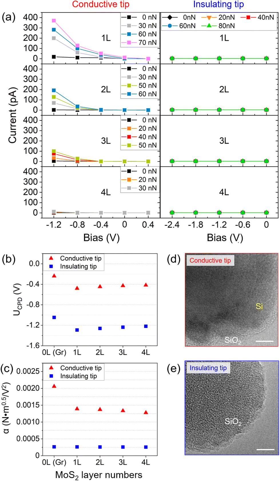 | ||
| Fig. 2 Comparison of a conductive and an insulating tip. (a) Electrical current as function of applied bias and applied load for the tips in contact with 1–4 layers MoS2 on graphene/SiC(0001). (b) Layer-dependence of the contact potential difference UCPD for conductive and insulating tip, determined by non-contact KPFM. (c) Strength of bias-dependent electrostatic tip–sample interaction α for 1–4 layers of MoS2 and the underlying graphene/SiC(0001), determined by non-contact KPFM. (d) TEM image of a conductive tip with crystalline structure of the Si(100) plane close to the apex. (e) TEM image of the insulating tip with amorphous structure of the apex (scale bars: 5 nm). | ||
A bias voltage applied between sample and tip is expected to increase their electrostatic attraction. We have combined friction force microscopy with non-contact Kelvin Probe Force Microscopy using the same AFM tip to determine the bias voltage at which the electrostatic attraction is minimized. The minimum indicates that the contact potential difference is compensated and reveals the work function difference between tip and sample. Fig. 2b compares the contact potential difference UCPD between tip and sample for the conductive and the insulating tip. There is constant offset of 0.81 V between the two tips for all surface layers, which confirms a constant difference in the work function between tips. The relative shift of the work function for different numbers of MoS2 layers with respect to the graphene/SiC(0001) is the same for both tips, the values are provided in Table 1. Performing these experiments in ultrahigh vacuum ensures that the values are not affected by water as the most critical adsorbent.35
| 1L | 2L | 3L | 4L |
|---|---|---|---|
| −242 mV | −210 mV | −188 mV | −174 mV |
In Kelvin Probe Force Microscopy (KPFM), the bias dependence of the electrostatic tip–sample attraction is measured as negative frequency shift of the cantilever's resonance. The normalized frequency shift36 has a parabolic dependence on the applied bias Δf/f0kA3/2 = −α(U − UCPD)2. Fig. 2c shows that the strength of the electrostatic tip–sample attraction is at least a factor of three smaller for the insulating tip and does not vary when measured on graphene or 1 to 4 layers of MoS2. In contrast, the conductive tip has a significantly stronger interaction with graphene and shows a slight decrease in interaction with increasing number of MoS2 layers.
Transmission electron microscopy (TEM) delivers insights into the structure of the AFM tip apex. While the conductive tip exhibits the regular atomic lattice of the Si(001) plane up to 2 nm below the tip end (Fig. 2d), the insulating tip exhibits the amorphous oxide structure for at least ten nanometers from the tip end (Fig. 2e). Such a thick oxide at the apex is result of the micro-fabrication process and typical for un-used tips, but is easily lost in the process of imaging larger areas to find MoS2 islands of different height. Tips were imaged by TEM immediately after the friction experiments on different MoS2 islands.
The dependence of the DMT parameters on the applied bias voltage and on the number of MoS2 layers is summarized in Fig. 3 for one conductive and one insulating tip. For the conductive tip, the DMT friction coefficient μDMT shows a minimum around the compensated contact potential UCPD, with a decrease of about 5% with respect to ±0.8 V bias. The adhesion parameter γ exhibits a weak maximum at UCPD. We note that these bias dependencies do not take the parabolic form which is always observed for the electrostatic attraction in non-contact mode. While μDMT decreases by about 15% from 1 to 4 layers of MoS2, the adhesion γ drops linearly to almost zero.
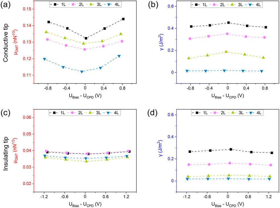 | ||
| Fig. 3 Graphical summary of parameters describing the load dependence of friction in the DMT model for 1–4 layers of MoS2 on graphene/SiC(0001) for (a and b) a conductive tip and (c and d) an insulating tip. (a and c) Bias-dependence of the DMT friction coefficient μDMT. (b and d) Bias-dependence of the adhesion parameter γ. | ||
For the insulating tip, μDMT exhibits a much weaker minimum at the compensated contact potential UCPD and also a much weaker dependence on the number of MoS2 layers (Fig. 3c). The bias dependence of the adhesion is also weaker, but a strong dependence on the number of MoS2 layers lets γ decays towards zero for 1 to 4 layers.
The dependence of friction on the number of MoS2 layers is compared with that for the graphene/SiC(0001) substrate in Fig. 4 for three different conductive tips and one insulating tip. The DMT friction coefficient μDMT is more than six times higher on 1 layer of MoS2 than on the underlying graphene/SiC(0001), it is also more than three times higher for the conducting tips than for the insulating tip on graphene/SiC(0001) and on 1 layer of MoS2. For all conductive tips, μDMT takes a reduced value on 4 layers of MoS2. The adhesion parameter γ is close to zero on graphene/SiC(0001) for all tips. On MoS2, it takes values of up to 500 mJ m−2, or 300 mJ m−2 for the insulating tip, and decays strongly from 1 to 4 layers.
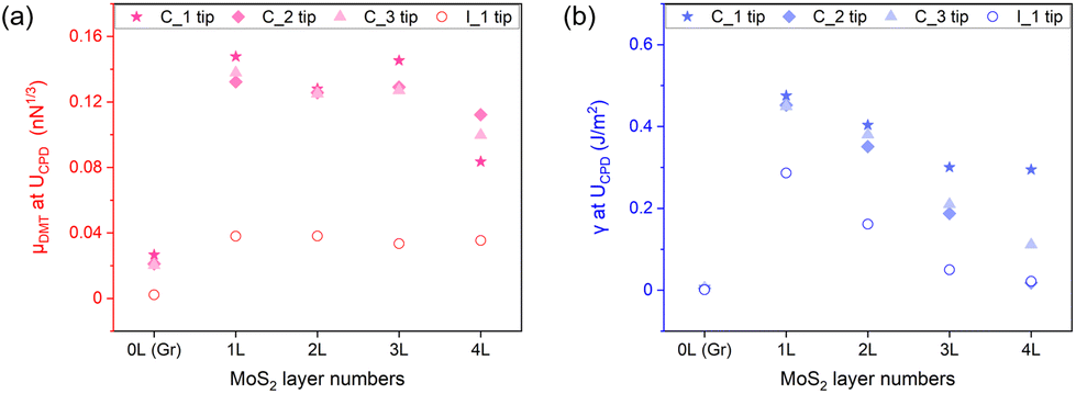 | ||
| Fig. 4 Layer-dependence of the parameters describing the load dependence of friction in the DMT model at compensated contact potential for three conductive tips (full symbols) and one insulating tip (hollow symbol). | ||
2. Discussion
The experimental results for the SiOx tip sliding on MoS2/graphene/SiC(0001) can be summarized in three key observations: the decrease of friction on an increasing number of MoS2 layers is caused mostly by a decrease of adhesion and less by a decrease of shear stress, an applied bias voltage affects the shear stress but not the adhesion, and the effect of the bias voltage depends strongly on the thickness of the oxide layer on the tip.The dominance of adhesion in the layer-dependence of friction on MoS2 is revealed by the offset between friction vs. load curves for different layer number, where the curves have a similar slope (Fig. 1b). Similar characteristics have been reported before for experiments on MoS2 of varying thickness in ambient conditions14,15,37,38 and are confirmed here for measurements in ultrahigh vacuum on CVD-grown MoS2. The strong decrease of adhesion from 1 to 4 layers of MoS2, almost to zero for most tips (Fig. 4b), cannot be attributed to the screening of electrostatic adhesion, since there is almost no bias dependence of adhesion (Fig. 3b and d). We rather suggest that out-of-plane deformation of the MoS2 layers leads to a conformation of the layers to the tip apex shape, thus to a larger contact area, and consequently to higher friction. This so-called ‘puckering’ effect is reduced with increasing number of MoS2 layers due to the increasing bending stiffness.8,37 The interaction of MoS2 with the graphene is expected to be weak (0.15 mJ m−2)39 compared to the interaction between MoS2 layers (0.55 mJ m−2).40 Fang et al. have suggested that the layer-dependence of friction depends on the tip shape, when friction depends on both shear stress and effects of out-of-plane deformation.41 In terms of their arguments, the layer dependence of friction on MoS2 in our experiments is dominated by the out-of-plane deformation caused by a sharp AFM tip. A contribution of out-of-plane deformation to friction is not expected for the epitaxial graphene layer, which is more strongly bound to the graphitic termination of the SiC(0001) substrate.42 This expectation is confirmed by the absence of any significant adhesion on graphene/SiC(0001) for all tips (Fig. 4b).
The tip-specific friction coefficient μDMT exhibits only a weak decrease with increasing number of MoS2 layers (Fig. 4a). This weaker dependence of μDMT on the number of layers confirms that the variation in friction can mostly be attributed to a variation of the effective adhesion γ, and not to a variation of the effective compliance 1/Eeff2/3. The weak dependence of μDMT also indicates that there is no strong variation of Eeff with the number of layers. The parameter μDMT reports the load dependence of friction and we conclude with Vazirisereshk et al.15 that the dominating physical property is the load-dependent atomic potential corrugation which impedes the lateral sliding. In agreement with their atomistic simulations, the coefficient μDMT is significantly smaller for graphene than for MoS2. Lavini et al. have noted that the in-plane polarization of each MoS2 layer may cause a difference in friction between odd numbers of MoS2 layers and even-numbered ones with no net polarization.14 The coefficient of load dependence μDMT indeed shows such an odd/even contrast for all conductive tips (Fig. 4a). For our system of large single-crystal islands of MoS2, the odd/even contrast does not reflect charges at the edges of MoS2 islands but rather contrasts in the load-dependence of the potential corrugation.
Friction is lower when the applied bias voltage compensates contact potential difference between tip and sample (Fig. 3), which was determined as UCPD in the non-contact KPFM mode. This bias dependence of friction is observed only at higher load, while friction at zero applied normal force does not show the bias dependence (Fig. 1b). Although our KPFM experiments reveal that there must be an electrostatic contribution to adhesion, is appears to be a negligible contribution for bias voltages ±1.2 V around UCPD. We suggest that the bias dependence of friction originates in an increase of the potential corrugation when the in-plane polarization of the MoS2 layers is distorted in the external normal electric field.
The shift in work function between graphene/SiC(0001) and MoS2/graphene/SiC(0001) of −242 mV is of the same order as the one reported by Forti et al. for WSe2 on the same substrate, who explained the overall electronic structure in terms of pinning by the n-doping in the graphene layer on SiC(0001).43 The shift in work function of 30 mV between 1L and 2L and then between subsequent layers is smaller than reported for MoS2 flakes on SiOx44 and smaller than for MoS2/graphene/SiC(0001) recorded in ambient conditions, where charged adsorbates influence the work functions.14
Contact potential difference UCPD, conductivity of the contact with the MoS2 layers, and the bias-dependence of electrostatic tip–sample attraction depend critically on the oxide thickness at the tip apex (Fig. 2). While no current was detected through contacts with the 10 nm oxide tip, a tunneling current was measured for the 2 nm oxide tip where the current increased super-linearly with applied bias. This characteristic has been explained by Liao et al. for a metal tip in contact with MoS2/graphite as thermally emitted current across a Schottky barrier.45 The authors attributed the load dependence of the current (Fig. 2a) not only to a variation of the contact area but also to a decrease of the Schottky barrier with increasing pressure. We find that the current is greatly reduced for thicker MoS2 layers and suggest that the tunneling probability across multi-layer MoS2 may be further reduced by the band gap expected for negative sample bias.28,46
The oxide at the tip also has a strong influence on friction and its bias dependence. While the adhesion γ is of similar magnitude and shows the same dependence on the number of MoS2 layers (Fig. 4b) for insulating and conductive tips, the tip-specific coefficient μDMT is by a factor of three lower and does not show any layer dependence for the insulating tip. Furthermore, the bias dependence of μDMT (Fig. 3a) is flat for the insulating tip (Fig. 3b). Please note that compensation of the work function minimizes the electrostatic attraction but does not cancel electric fields across the contact. This is manifest by the observation of significant electrical current through the conductive tip at an applied bias of −0.4 V (Fig. 2a), which is the compensating bias for this tip (Fig. 2b). However, no current is measured through the insulating tip at the higher bias of −1.2 V, which is the compensating bias for this tip.
These observations support our picture of the underlying mechanisms. The adhesion is dominated not by electrical tip properties but by out-of-plane deformations of MoS2 layers towards the shape of the tip apex, with a smaller resulting contact area for the tip whose sharp oxide is not worn off. The friction coefficient μDMT is sensitive to an enhancement of the atomic potential corrugation in the applied electric field, which is rather weak when the potential is applied across an tip oxide as thick as 10 nm.
3. Conclusions
In conclusion, the combination of non-contact Kelvin Probe Force Microscopy with contact-mode friction force microscopy in ultra-high vacuum has revealed the mechanisms of nanoscale friction on ultra-thin layers of MoS2 grown on graphene/SiC(0001). The overall strength of friction is dominated by adhesion which is mediated by a deformation of MoS2 to adapt the tip shape. Friction decreases with increasing number of MoS2 layers as the bending rigidity leads to less deformation. The dependence of friction on applied load and bias voltage can be attributed to variations in the atomic potential corrugation of the MoS2/SiOx interface, which is enhanced by both load and bias. The results enrich our understanding of the mechanical properties of heterostructures of 2D materials and thus contribute to a rational design of lubricating interfaces built from this new class of materials.4. Experimental methods
Sample preparation
The stacked MoS2/graphene heterostructure is fabricated by a two-step procedure. First, the monolayer graphene is prepared ex situ on SiC(0001) surface via the high-temperature (around 1560–1570 °C) graphitization in an Ar atmosphere of 900 mbar.27 Then, 1–4 layer MoS2 crystals were grown on the epitaxial graphene in a chemical vapor deposition (CVD) reactor at 680 °C using a method reported previously.25 No additional cleaning procedures were applied after transfer of the samples to the UHV AFM chamber. After finishing all experiments, we heated the sample in UHV to a temperature of about 550 K for 2 hours and confirmed in additional experiments that surface structure and AFM results were still comparable to those recorded on as-grown samples.Atomic/friction force microscopy experiments
All the experiments were performed in a custom-built UHV AFM (Omicron, VT AFM XA) at room temperature. The softer PPP-CONT silicon cantilevers (Nanosensor, the nominal spring constant kn = 0.2 N m−1 and the first flexural frequency f1 = 12 kHz) were used for both topography/bias and the friction force measurement. The scanning strategy is to search for flat areas with MoS2 islands of different height by means of large-area non-contact mode AFM. We then limit the scanning to that flat area using low-load friction and KPFM experiments to preserve the tip structure for comparability between islands with different number of layers. The normal and lateral forces were calibrated with the sensitivity of the photodetector (obtained from the force–distance curve)47 and the cantilever dimensions (measured by the scanning electron microscope at 10 kV, FEI Quanta 400 SEM). Additionally, the tip structure was analyzed after friction and KPFM experiments with a transmission electron microscope at 200 kV (JEM-2100 LaB6 TEM). The applied normal load ranges from 0 to 120 nN within the elasticity of the selected 2D materials.48 The scanning speed was set as 20 nm s−1 for the whole experiment. Notably, the friction force were calculated from the average lateral force between the first half of forward curve and the second half of the backward curve. It will effectively avoid the seriously tilted slopes of the normal-frictional curves at higher loads (see Fig. S4†), i.e. the underestimation of the friction force.Furthermore, Kelvin probe force microscopy (KPFM) was carried out to measure the contact potential differences (UCPD) between tip and sample surfaces, which is related to the tip–sample electrostatic force Fel as below:
 | (2) |
As we know in the nc-AFM, the frequency shift Δf can be used to describe tip–sample interaction, which is proportional to the tip–sample force and distance 〈Fts·z〉. To factor out the dependence on the experimental parameters, it can be normalized as below:
 | (3) |
| Γ = Γ0 − α(UBias − UCPD)2. | (4) |
Author contributions
Z. L. and R. B. conceived the original idea and the experiments. J. M. J. L., A. G., Z. G. and A. T. prepared the MoS2/graphene/SiC(0001) heterostructure samples. Z. L. and B. S. performed the AFM and FFM experiments. Z. L., R. B. and B. S. wrote the manuscript. All authors discussed the results and revised the manuscript.Conflicts of interest
There are no conflicts to declare.Acknowledgements
This project has been funded by Deutsche Forschungsgemeinschaft within the Priority Program SPP 2244 ‘2DMP’.References
- A. K. Geim and I. V. Grigorieva, Nature, 2013, 499, 419–425 CrossRef CAS PubMed.
- K. S. Novoselov, A. Mishchenko, A. Carvalho and A. H. Castro Neto, Science, 2016, 353, aac9439 CrossRef CAS PubMed.
- C. R. Woods, F. Withers, M. J. Zhu, Y. Cao, G. Yu, A. Kozikov, M. Ben Shalom, S. V. Morozov, M. M. van Wijk, A. Fasolino, M. I. Katsnelson, K. Watanabe, T. Taniguchi, A. K. Geim, A. Mishchenko and K. S. Novoselov, Nat. Commun., 2016, 7, 10800 CrossRef CAS PubMed.
- J. M. Martin, C. Donnet, T. Lemogne and T. Epicier, Phys. Rev. B: Condens. Matter Mater. Phys., 1993, 48, 10583–10586 CrossRef CAS PubMed.
- M. Dienwiebel, G. S. Verhoeven, N. Pradeep, J. W. Frenken, J. A. Heimberg and H. W. Zandbergen, Phys. Rev. Lett., 2004, 92, 126101 CrossRef.
- T. Filleter, J. L. McChesney, A. Bostwick, E. Rotenberg, K. V. Emtsev, T. Seyller, K. Horn and R. Bennewitz, Phys. Rev. Lett., 2009, 102, 086102 CrossRef CAS PubMed.
- D. Berman, A. Erdemir and A. V. Sumant, Carbon, 2013, 54, 454–459 CrossRef CAS.
- C. Lee, Q. Li, W. Kalb, X.-Z. Liu, H. Berger, R. W. Carpick and J. Hone, Science, 2010, 328, 76–80 CrossRef CAS.
- H. Li, J. H. Wang, S. Gao, Q. Chen, L. M. Peng, K. H. Liu and X. L. Wei, Adv. Mater., 2017, 29, 1701474 CrossRef PubMed.
- M. Liao, P. Nicolini, L. Du, J. Yuan, S. Wang, H. Yu, J. Tang, P. Cheng, K. Watanabe, T. Taniguchi, L. Gu, V. E. P. Claerbout, A. Silva, D. Kramer, T. Polcar, R. Yang, D. Shi and G. Zhang, Nat. Mater., 2022, 21, 47–53 CrossRef CAS PubMed.
- O. Hod, E. Meyer, Q. Zheng and M. Urbakh, Nature, 2018, 563, 485–492 CrossRef CAS PubMed.
- M. Wolloch, G. Levita, P. Restuccia and M. Righi, Phys. Rev. Lett., 2018, 121, 026804 CrossRef CAS PubMed.
- Y. M. Song, D. Mandelli, O. Hod, M. Urbakh, M. Ma and Q. S. Zheng, Nat. Mater., 2018, 17, 894–899 CrossRef CAS PubMed.
- F. Lavini, A. Calò, Y. Gao, E. Albisetti, T. Cao, G. Li, L. Cao, C. Aruta and E. Riedo, et al. , Nanoscale, 2018, 10, 8304–8312 RSC.
- M. R. Vazirisereshk, H. Ye, Z. J. Ye, A. Otero-de-la Roza, M. Q. Zhao, Z. L. Gao, A. T. C. Johnson, E. R. Johnson, R. W. Carpick and A. Martini, Nano Lett., 2019, 19, 5496–5505 CrossRef CAS.
- K. Huang, H. Qin, S. Zhang, Q. Li, W. Ouyang and Y. Liu, Adv. Funct. Mater., 2022, 32, 2204209 CrossRef CAS.
- S. Zhang, Q. Yao, L. Chen, C. Jiang, T. Ma, H. Wang, X.-Q. Feng and Q. Li, Phys. Rev. Lett., 2022, 128, 226101 CrossRef CAS PubMed.
- A. Song, R. Shi, H. Lu, X. Wang, Y. Hu, H.-J. Gao, J. Luo and T. Ma, Nano Lett., 2022, 22, 1889–1896 CrossRef CAS PubMed.
- H. Lang, Y. Peng, X. Cao and K. Zou, ACS Appl. Mater. Interfaces, 2020, 12, 25503–25511 CrossRef CAS.
- X. Chen, Y. Huang, K. Zou and Y. Peng, Appl. Surf. Sci., 2022, 581, 152361 CrossRef CAS.
- K. Yu, K. Zou, H. Lang and Y. Peng, Friction, 2021, 9, 1492–1503 CrossRef CAS.
- Y. Zeng, F. He, Q. Wang, X. Yan and G. Xie, Appl. Surf. Sci., 2018, 455, 527–532 CrossRef CAS.
- C. Wang, W. Chen, Y. Zhang, Q. Sun and Y. Jia, Tribol. Lett., 2015, 59, 1–8 CrossRef CAS.
- J. Peng, F. Yang, K. Huang, H. Dong, S. Yan and X. Zheng, Phys. Lett. A, 2020, 384, 126166 CrossRef CAS.
- A. George, C. Neumann, D. Kaiser, R. Mupparapu, T. Lehnert, U. Hübner, Z. Tang, A. Winter, U. Kaiser and I. Staude, et al. , J. Phys. Mater., 2019, 2, 016001 CrossRef CAS.
- S. Shree, A. George, T. Lehnert, C. Neumann, M. Benelajla, C. Robert, X. Marie, K. Watanabe, T. Taniguchi, U. Kaiser, B. Urbaszek and A. Turchanin, 2D Mater., 2020, 7, 015011 CrossRef CAS.
- M. H. Oliveira, T. Schumann, M. Ramsteiner, J. M. J. Lopes and H. Riechert, Appl. Phys. Lett., 2011, 99, 111901 CrossRef.
- X. Liu, I. Balla, H. Bergeron, G. P. Campbell, M. J. Bedzyk and M. C. Hersam, ACS Nano, 2016, 10, 1067–1075 CrossRef CAS PubMed.
- Y. Kobayashi, T. Taniguchi, K. Watanabe, Y. Maniwa and Y. Miyata, Appl. Phys. Express, 2017, 10, 045201 CrossRef.
- M. Z. Liao, Z. W. Wu, L. J. Du, T. T. Zhang, Z. Wei, J. Q. Zhu, H. Yu, J. Tang, L. Gu, Y. X. Xing, R. Yang, D. X. Shi, Y. G. Yao and G. Y. Zhang, Nat. Commun., 2018, 9, 4068 CrossRef PubMed.
- J. Gao, W. D. Luedtke, D. Gourdon, M. Ruths, J. N. Israelachvili and U. Landman, J. Phys. Chem. B, 2004, 108, 3410–3425 CrossRef CAS.
- T. Filleter, K. V. Emtsev, T. Seyller and R. Bennewitz, Appl. Phys. Lett., 2008, 93, 133117 CrossRef.
- B. Derjaguin, V. Muller and Y. Toporov, J. Colloid Interface Sci., 1975, 53, 314–326 CrossRef CAS.
- D. Andersson and A. S. de Wijn, Nat. Commun., 2020, 11, 420 CrossRef CAS.
- S. Y. Lee, U. J. Kim, J. Chung, H. Nam, H. Y. Jeong, G. H. Han, H. Kim, H. M. Oh, H. Lee, H. Kim, Y.-G. Roh, J. Kim, S. W. Hwang, Y. Park and Y. H. Lee, ACS Nano, 2016, 10, 6100–6107 CrossRef CAS.
- F. J. Giessibl, Phys. Rev. B: Condens. Matter Mater. Phys., 1997, 56, 16010–16015 CrossRef CAS.
- P. Huang, A. Castellanos-Gomez, D. Guo, G. Xie and J. Li, J. Phys. Chem. C, 2018, 122, 26922–26927 CrossRef CAS.
- D. L. C. Ky, B.-C. Tran Khac, C. T. Le, Y. S. Kim and K.-H. Chung, Friction, 2018, 6, 395–406 CrossRef CAS.
- M.-Q. Le, Meccanica, 2017, 52, 307–315 CrossRef.
- Z. Fang, X. Li, W. Shi, Z. Li, Y. Guo, Q. Chen, L. Peng and X. Wei, J. Phys. Chem. C, 2020, 124, 23419–23425 CrossRef CAS.
- L. Fang, D.-M. Liu, Y. Guo, Z.-M. Liao, J.-B. Luo and S.-Z. Wen, Nanotechnology, 2017, 28, 245703 CrossRef PubMed.
- Q. Y. Li, C. Lee, R. W. Carpick and J. Hone, Phys. Status Solidi B, 2010, 247, 2909–2914 CrossRef CAS.
- S. Forti, A. Rossi, H. Buch, T. Cavallucci, F. Bisio, A. Sala, T. O. Mentes, A. Locatelli, M. Magnozzi, M. Canepa, K. Mueller, S. Link, U. Starke, V. Tozzini and C. Coletti, Nanoscale, 2017, 9, 16412–16419 RSC.
- O. Ochedowski, K. Marinov, N. Scheuschner, A. Poloczek, B. K. Bussmann, J. Maultzsch and M. Schleberger, Beilstein J. Nanotechnol., 2014, 5, 291–297 CrossRef.
- M. Liao, L. Du, T. Zhang, L. Gu, Y. Yao, R. Yang, D. Shi and G. Zhang, Chin. Phys. B, 2019, 28, 017301 CrossRef CAS.
- X. Dong, C. Yan, D. Tomer, C. H. Li and L. Li, Appl. Phys. Lett., 2016, 109, 051604 CrossRef.
- B. Bhushan, Wear, 2005, 259, 1507–1531 CrossRef CAS.
- A. Klemenz, L. Pastewka, S. G. Balakrishna, A. Caron, R. Bennewitz and M. Moseler, Nano Lett., 2014, 14, 7145–7152 CrossRef CAS.
Footnotes |
| † Electronic supplementary information (ESI) available: Atomic friction maps. See DOI: https://doi.org/10.1039/d3nr00138e |
| ‡ Present address: School of Materials Science and Engineering, Nankai University, 300350 Tianjin, China. |
| This journal is © The Royal Society of Chemistry 2023 |