
 Open Access Article
 This Open Access Article is licensed under a Creative Commons Attribution-Non Commercial 3.0 Unported Licence
Hyperdoped Si nanocrystals embedded in silica for infrared plasmonics†
Meiling
Zhang
a,
Jean-Marie
Poumirol
a,
Nicolas
Chery
a,
Hervé
Rinnert
 b,
Alaa E.
Giba
bc,
Rémi
Demoulin
d,
Etienne
Talbot
d,
Fuccio
Cristiano
e,
Teresa
Hungria
f,
Vincent
Paillard
a,
Fabrice
Gourbilleau
g and
Caroline
Bonafos
*a
b,
Alaa E.
Giba
bc,
Rémi
Demoulin
d,
Etienne
Talbot
d,
Fuccio
Cristiano
e,
Teresa
Hungria
f,
Vincent
Paillard
a,
Fabrice
Gourbilleau
g and
Caroline
Bonafos
*a
aCEMES-CNRS, Université de Toulouse, CNRS, 31055 Toulouse, France. E-mail: caroline.bonafos@cemes.fr
bUniversité de Lorraine CNRS, IJL, Nancy, France
cNational Institute of Laser Enhanced Sciences, Cairo University, Giza 12613, Egypt
dNormandie Univ, UNIROUEN, INSA Rouen, CNRS, Groupe de Physique des Matériaux, 76000 Rouen, France
eLAAS-CNRS, Université de Toulouse, CNRS, 31031 Toulouse, France
fCentre de Microcaractérisation Raimond Castaing (UAR 3623), 31400 Toulouse, France
gCIMAP, Normandie Univ, ENSICAEN, UNICAEN, CEA, CNRS, 6 Boulevard Maréchal Juin, 14050, Caen Cedex 4, France
First published on 10th March 2023
Abstract
We present the experimental realization of plasmonic hyperdoped Si nanocrystals embedded in silica via a combination of sequential low energy ion implantation and rapid thermal annealing. We show that phosphorus dopants are incorporated into the nanocrystal cores at concentrations up to six times higher than P solid solubility in bulk Si by combining 3D mapping with atom probe tomography and analytical transmission electron microscopy. We shed light on the origin of nanocrystal growth at high P doses, which we attribute to Si recoiling atoms generated in the matrix by P implantation, which likely increase Si diffusivity and feed the Si nanocrystals. We show that dopant activation enables partial nanocrystal surface passivation that can be completed by forming gas annealing. Such surface passivation is a critical step in the formation of plasmon resonance, especially for small nanocrystals. We find that the activation rate in these small doped Si nanocrystals is the same as in bulk Si under the same doping conditions.
Introduction
Localized surface plasmon resonances (LSPR) caused by collective oscillations of free carriers on metal surfaces have been studied for decades because of their ability to fundamentally alter light–matter interactions with remarkable applications in enhanced spectroscopy, sensing, optical devices, and photovoltaics.1–3 Because of their strong LSPR in the visible range, nanostructures of noble metals such as gold or silver have long been used in plasmonics-based technology.4–6 However, large structures must be considered to achieve resonances in the infrared (IR) range,7 which presents a challenge for integration into electronic semiconductor-based devices. This has recently begun to change with the discovery of LSPR in doped semiconductors, which has resulted in mid-infrared (MIR) plasmon resonance.8,9 In this case, the dopant concentration becomes a new parameter for adjusting the resonance position.8 However, doping nanostructures remains a challenge that is far from being mastered. Indeed, doping at the nanoscale is difficult due to mechanisms such as thermodynamic stability and self-purification.10 Among semiconductors, silicon (Si) is of particular interest due to its low production cost, abundance, and non-toxicity. Furthermore, with available carrier concentrations of up to a few 1019 cm−3 after doping, massively doped Si nanostructures are excellent candidates for mass production of highly integrated low-cost MIR plasmonic devices.9Using top down and non-equilibrium approaches, ordered arrays of large (100 nm) hyperdoped Si nanodisks with a tunable LSPR in the MIR up to the near infrared (NIR) range were recently realized from the nanostructuration of heavily doped silicon-on-insulator (SOI) layers.11,12 In terms of nanoscale doping, freestanding small (10 nm) plasmonics Si nanocrystals (SiNCs) fabricated by non-equilibrium methods and randomly doped with phosphorus or boron at the nanoscale have been successfully achieved.13–18 However, their plasmonic properties remain extremely sensitive to oxidation, raising concerns about reproducibility, stability, and aging. Our group recently synthesized massively doped small (10 nm) SiNCs embedded in a silica matrix using a combination of sequential low energy ion implantation and rapid thermal annealing (RTA). We showed that such embedded nanostructures can support LSPR with only about 10 free electrons per nanocrystal, confirming theoretical predictions and probing the collective nature of plasmons.19 Such small hyperdoped SiNCs raise fundamental questions such as dopant localization inside the NCs (volume/surface), the effect of doping on the NC growth mechanism, the effect of NC size on the dopant solubility limit and the resulting activation rate, or the impact of the NC surface defective state on the plasmonic properties, all of which must be addressed in order to optimize their plasmonic properties.
In this paper, we investigate the two-way interactions between phosphorus (P) doping impurities and their host SiNCs embedded in a silica matrix, with one side focusing on the effect of hyperdoping on the structural properties of the NCs and the inverse effect of nanoscale on doping efficiency. Doping impurities were incorporated in the SiNC core at concentrations well above the bulk solubility limit. Low activation rates of less than 5% were measured, which are comparable to bulk Si under identical annealing conditions and sufficient to induce a plasmon resonance. High P doses cause an increase in the SiNCs size, which is attributed to the presence of Si recoiling atoms in the matrix as a result of P implantation. The light emission properties of SiNCs were investigated to determine their surface quality, revealing the passivation of Si dangling bonds at the NC surface with electron charges provided by activated impurities, as well as further improvement by forming gas (FG) annealing. We demonstrate that this surface passivation is a critical step in the appearance of LSPR in the case of small NCs.
Experimental
Undoped and P-doped SiNCs embedded in SiO2 were synthesized by sequential low energy ion implantation. A 200 nm thick thermal silica layer on top of a silicon substrate was implanted with Si+ ions at 8 keV and a dose of 2 × 10¹⁶ ions per cm2. Embedding the SiNCs in a silica matrix is expected to provide a passivation route that reduces surface defect states, to protect the NCs from aging, and thus contribute to the stability of their plasmonic properties. An intermediate RTA was performed for 60 seconds at 1050 °C in N2 dedicated to the nucleation of SiNCs. This thermal budget was optimized for the nucleation and crystallization of SiNCs in SiO2.20 To match the projected Si range, P was implanted at 7 keV with 5 doses ranging from 1015 to 3 × 10¹⁵ ions per cm2. The nominal P/Si dose ratio ranges from 5 to 15%. After P implantation, the samples were annealed again at 1050 °C for 60 seconds in N2. Half of each sample was annealed at 500 °C for 900 seconds under forming gas (90% N2 + 10% H2) to improve the surface passivation of SiNCs. The implantation and annealing conditions are summarized in Table 1.| Nominal P implanted dose (ions per cm2) | P/Si nominal ratio (%) | Nucleation annealing (N2) | Activation annealing (N2) | FG annealing | |
|---|---|---|---|---|---|
| P0 | 0 | 0 | 1050 °C 60 s | — | — |
| P0FG | 0 | 0 | 1050 °C 60 s | — | 500 °C 900 s |
| P1 | 1.0 × 10¹⁵ | 5.0 | 1050 °C 60 s | 1050 °C 60 s | — |
| P1FG | 1.0 × 10¹⁵ | 5.0 | 1050 °C 60 s | 1050 °C 60 s | 500 °C 900 s |
| P2 | 1.5 × 10¹⁵ | 7.5 | 1050 °C 60 s | 1050 °C 60 s | — |
| P2FG | 1.5 × 10¹⁵ | 7.5 | 1050 °C 60 s | 1050 °C 60 s | 500 °C 900 s |
| P3 | 2.0 × 10¹⁵ | 10.0 | 1050 °C 60 s | 1050 °C 60 s | — |
| P3FG | 2.0 × 10¹⁵ | 10.0 | 1050 °C 60 s | 1050 °C 60 s | 500 °C 900 s |
| P4 | 2.5 × 10¹⁵ | 12.5 | 1050 °C 60 s | 1050 °C 60 s | — |
| P4FG | 2.5 × 10¹⁵ | 12.5 | 1050 °C 60 s | 1050 °C 60 s | 500 °C 900 s |
| P5 | 3.0 × 10¹⁵ | 15.0 | 1050 °C 60 s | 1050 °C 60 s | — |
| P5FG | 3.0 × 10¹⁵ | 15.0 | 1050 °C 60 s | 1050 °C 60 s | 500 °C 900 s |
A TECNAI F20 SACTEM was used to obtain high resolution electron microscopy (HREM) and energy filtered transmission electron microscopy (EFTEM) images. It is equipped with a spherical aberration corrector located below the objective lens, leading to a spatial resolution of 1.2 Å. Scanning TEM-energy dispersive X-ray spectroscopy (STEM-EDX) measurement was carried out using a JEOL ARM cold FEG microscope equipped with a probe spherical aberration corrector at 200 kV with a STEM resolution of 78 pm. For EDX measurements, a CENTURIO-X detector with an elevation angle of 24.3 degrees and a collection angle of 0.98 steradians was used. The probe size used for our experiment is 0.8 Å and the detection limit is between 0.2 and 0.5 at%. Measuring the P content inside the SiNCs embedded in a SiO2 matrix is a critical issue that requires a specific methodology for distinguishing between the part that belongs to the NCs and the part that belongs to their matrix shell for both Si and P elements. On a reference sample of bulk Si implanted with P at high doses, the Cliff-Lorimer coefficient was determined.12 Considering that SiNCs contain no oxygen, the total number of P, Si, and O atoms in the NCs region can be expressed as a function of SiNC volume fraction, this later being easily deduced from the O atom ratio in the NC region and the matrix. Finally, the P content inside the SiNCs (% Pdop) can be simply expressed as a function of the Si (% SiNCregion, % SiSiO2), P (% PNCregion, % PSiO2) and O (% ONCregion, % OSiO2) raw atomic compositions measured in the NCs region and in the matrix, respectively:

For TEM observation and STEM-EDX analysis, lamellas thinned up to t/λ < 0.3 (ratio between the thickness t and the electron mean free path λ) were prepared by focused ion beam (FIB) using a FEI Helios Nanolab 600i dual beam microscope. Cross-sectional lamellas were prepared with a decreasing voltage from 16 kV–50 pA to 5 kV–15 pA. A thin (1–2 μm) platinum (Pt) protective layer was deposited on the region of interest. A very thin (100 nm) carbon layer was deposited between the sample surface and the platinum protective layer to prevent Pt diffusion into the SiO2 matrix.
A careful examination of the atomically resolved 3D images obtained by laser-assisted wide-angle atom probe tomography (APT) equipped with a femtosecond pulsed UV laser (λ = 343 nm, 350 fs, 33 nJ).21 The analyzes were performed in a high vacuum chamber at 10−10 mbar and at a temperature of 80 K. Sample tips were prepared using a Helios G4 CXe FIB from ThermoScientific. The processing of the APT data was carried out using GPM3Dsoft software. The detection limit is around 1019 at per cm3.
Photoluminescence (PL) measurements have been performed by using a 325 nm He–Cd laser as an excitation source. The PL signal was collected using a monochromator equipped with a 600 grooves per mm grating and measured with a cooled photomultiplier tube operating in the visible-NIR range. The obtained spectra were corrected for the system response.
Fourier transform infrared (FTIR) spectroscopy was used to study the plasmon resonances in the infrared range of doped SiNCs embedded in silica. The setup is a Bruker Vertex 70 spectrometer coupled to a Cassegrain microscope.
Results and discussion
Doping of Si nanostructures via physical routes such as ion implantation is typically accomplished by introducing dopant impurities into the matrix concurrently with Si supersaturation, prior to NC formation.21–23 The subsequent high temperature thermal treatment causes dopant incorporation and the formation of SiNCs. This method does not allow for the experimental decoupling of system equilibrium properties from kinetic effects. Significant efforts have recently been made to develop alternative approaches for doping SiNCs after their formation.22 We used the same approach here, but separated the NC nucleation and dopant activation steps using sequential low energy ion implantation of Si and P.Before doping, the Si nanocrystals are distributed along a 20 nm thick band (see Fig. 1(a) and (b)). The spatial distribution is bimodal (Fig. 1(d)) with large Si nanocrystals having a mean diameter of 4.5 nm and smaller ones having a mean diameter of 2.5 nm. The former are located at the implantation profile's projected range, while the latter are located deeper in the implantation profile tail. This spatial distribution is related to the Gaussian shape of the implantation profile. During the nucleation process, a higher volume density of SiNCs is formed in the projected range (Rp = 15 nm) of the implantation profile, where the reservoir of Si atoms is greater than in the profile tail. Because the residual supersaturation in the matrix remains higher at Rp than in the tail regions, these NCs are likely to grow faster during the subsequent pure growth process. Finally, during the Ostwald ripening, competitive growth differs between Si nanocrystals at the implanted profile's peak and those in the tails. The overlapping of diffusion fields between close neighboring NCs causes enhanced Ostwald ripening at the profile maximum, where the NC density is high.23 In comparison, the low volume density of SiNCs in the profile tails grows in accordance with a classical Ostwald ripening process (mean field approximation), resulting in smaller SiNCs. It is worth noting that a low density of small SiNCs was expected to form on the surface, but oxygen diffusion from moisture most likely reduced the supersaturation available for their formation.24
 | ||
| Fig. 1 (a) and (e) EFTEM cross-sectional images displaying the spatial distribution of undoped (P0) and doped (P4FG) SiNCs with associated SRIM profiles for Si (red line) and P (blue line). Zoom-in on the NC region for (b) the undoped and (f) doped samples, with associated EDX profiles for Si (red line), O (green line) and P (blue line). (c) and (g) HREM images of a large SiNC in the (110) zone axis. NC average shifted histograms (ASH)25 showing the bimodal size distributions for the undoped (d) and doped (h) samples. | ||
High resolution TEM observations of single NCs show that they are indeed crystalline, with the expected lattice parameter of Si (0.543 nm). Most of the observed NCs are in the [110] zone axis as the one shown in Fig. 1(c), with interatomic distances of 0.31 nm corresponding to the (111) planes.
Bimodal spatial (Fig. 1(e) and (f)) and size (Fig. 1(h)) distributions were also found in the case of P-doped SiNCs, regardless of the dopant doses, as shown for the example of P4FG and for different implanted doses (Fig. S3 of the ESI†). The HREM image (Fig. 1(g)) shows that the NCs are still crystalline after P implantation and activation annealing with lattice distances of 0.31 nm corresponding to the (111) planes. Strain measurement has been performed on the HREM images of single P-doped SiNCs using the method developed in ref. 26 and 27. Maps of strain components inside the nanocrystal have been extracted with respect to the Bravais lattice of Si. Very low contraction values have been found for the in plane (εx′x′), out of plane (εz′z′) and shear (εx′z′) strain components. Hence, for the highest implanted dose (P5FG) average values as low as −0.05%, −0.03% and −0.02% for respectively (εx′x′), (εy′y′), and (εx′y′) have been measured (see Fig. S1 of the ESI†). This result is consistent with the fact that P and Si atoms have almost the same covalent radius (1.07 Å and 1.11 Å, respectively),28 resulting in a very low contraction coefficient of the lattice parameter when incorporating P in Si, even at a high content (Δa/a = −0.009 for 10 at% P).29 Note that we observed the behavior of all implanted doses, and that no SixPy alloy (neither SiP nor SiP2)30 was found even at the highest investigated dose.
A careful examination of the atomically resolved 3D mapping obtained by laser-assisted APT (Fig. 2(a)) can reveal the precise location of the dopant. In Fig. 2(b) and (c), an example of atomic spatial distribution is shown for P4, revealing that the majority of P atoms (black dots) are well located inside the large SiNCs (Fig. 2(b)); meanwhile, almost no P atom has been detected inside the small ones at the profile tail (Fig. 2(c)) and only a few ones in the matrix.
 | ||
| Fig. 2 (a) APT 3D mapping with Si atoms in red for P4 demonstrating the spatial distribution of impurities. (b) Atomic distribution in the large SiNCs in the projected range (volume of the observed region is 16 × 16 × 4 nm3) and (c) in the small SiNCs located in the Si implantation profile tail (volume of the observed region is 17 × 17 × 4 nm3); black and red dots correspond to P and Si atoms, respectively. Erosion profiles displaying the spatial distribution of Si (red), O (green), and P (black) for large nanocrystals (d) and small nanocrystals (e), where the zero corresponds to the SiNCs/SiO2 interface. | ||
The precise location of dopants around the SiNCs was investigated by computing the erosion profile, as shown in Fig. 2(d) and (e). These profiles have been deduced by considering all the SiNCs present in the analyzed volumes. The oxygen (O) profile reveals the measurement of almost 20 at% of O in the core of SiNCs. This apparent O level is a well-known artifact that results in a local magnification effect31 between the Si and SiO2 phases caused by the artificial introduction of atoms from the surrounding matrix into the clusters, which consequently artificially lowers the measured concentration of P in the cluster core. From previous APT studies of P-doped SiNCs prepared using the same technique,21,32 we can state unequivocally that SiNCs do not contain any oxygen atoms. These profiles confirm that the dopants are incorporated in the core of SiNCs for the large nanocrystals (Fig. 2(d)); meanwhile, the P concentration in the core of SiNCs is zero for small nanocrystals (Fig. 2(e)) and the P atoms are mostly found at the interface. These erosion profiles also confirm that the matrix is SiO2 containing a slight Si excess. This result is consistent with the literature for P-doped SiNCs embedded in SiO2![[thin space (1/6-em)]](https://www.rsc.org/images/entities/char_2009.gif) 21,32,33 and with theoretical calculations that are presented in ref. 34 and 35. The position of P in the core of SiNCs contradicts self-purification theories10,36,37 but is in line with the well-known macroscopic behavior of these dopants at bulk Si/SiO2 interfaces, where phosphorus segregates in favor of Si at thermal equilibrium.38,39
21,32,33 and with theoretical calculations that are presented in ref. 34 and 35. The position of P in the core of SiNCs contradicts self-purification theories10,36,37 but is in line with the well-known macroscopic behavior of these dopants at bulk Si/SiO2 interfaces, where phosphorus segregates in favor of Si at thermal equilibrium.38,39
The P content of few individual SiNCs was measured on the APT images for P2 and P4 (Fig. 3). This content is negligible in the majority of the small SiNCs (diameter <3 nm) in the profile tail. The absolute number of P atoms inside SiNCs increases with NC size, with values exceeding 100 P atoms for diameters greater than 7 nm. The remaining P content in the matrix can be deduced from the depth profile in Fig. 2(d) and (e) and is approximately 0.5 at% (3.3 × 10²⁰ at per cm3). This value is higher than the detection limit of the technique (around 1019 at per cm3). However, due to the small size of the volume analyzed here, the low statistics on the images does not allow us to extract a reliable average value for the P concentration inside the SiNCs. A systematic and quantitative study of the evolution of P content inside the SiNCs as a function of implanted dose has been performed by STEM-EDX.
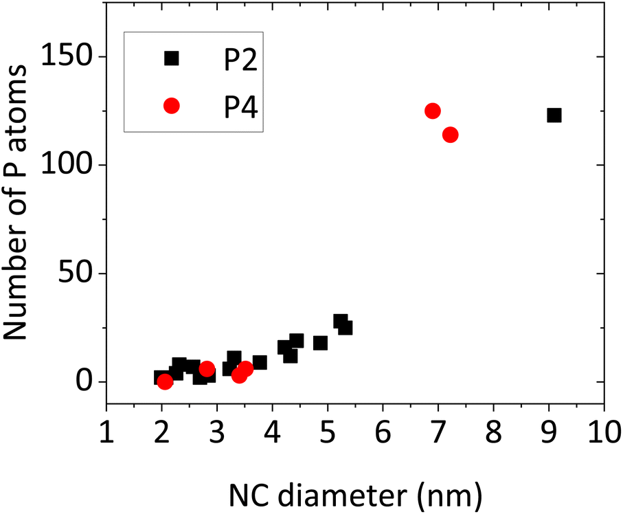 | ||
| Fig. 3 Number of P atoms inside the SiNCs as a function of the NC diameter for P2 (1.5 × 10¹⁵ ions per cm2) and P4 (2.5 × 10¹⁵ ions per cm2). | ||
The Si excess and O depletion in the NCs region are visible in the EDX profiles superimposed on the TEM picture in Fig. 1(f), as well as the presence of a P peak that coincides with the large SiNCs. The P concentration in the large SiNCs before and after FG annealing as a function of the implanted P dose is plotted in Fig. 4. The P concentration inside these SiNCs increases with P implanted dose, ranging from 2.7 × 10²¹ ± 8.1 × 10²⁰ at per cm3 (5.4 ± 1.6 at%) for P1 to 6.6 × 10²¹ ± 2.0 × 10²¹ at per cm3 (13.1 ± 3.9 at%) for P5. As we will see further, this increased P amount with the implanted dose has also an effect on the size of the large NCs. The P concentration in the matrix region measured by STEM-EDX is of around 0.5 at% independently of the implanted dose, in good agreement with the APT measurements.
 | ||
| Fig. 4 Average P content inside the large particles measured by STEM-EDX as a function of dose for samples annealed with FG (red spheres) and without FG annealing (black squares). | ||
Such concentrations of some at% are consistent with previous studies in the literature, which conclude that doping SiNCs in SiO2 corresponds to a thermodynamically favorable configuration.21,22,32,40 The measured P concentrations are indeed up to six times higher than the solid solubility of P in bulk Si at the same temperature (1.8 at%).41 However, it is impossible to conclude that the observed increase in the incorporated dopant concentration is due to an equilibrium property of SiNCs embedded in SiO2 described in ref. 22 or a kinetic effect. The dopants are introduced into the SiNCs from a spatially separated dopant source, the SiNCs being already formed before doping, which keeps the system in theory very close to thermodynamic equilibrium. Ion implantation is an out-of-equilibrium process that allows for the introduction of impurity concentrations far above the solubility limit in a matrix. Furthermore, the short annealing duration for dopant activation (60 seconds only) prevents the system from returning to thermodynamic equilibrium.
Concerning now the small SiNCs formed in the profile tail, where the implanted P concentration is low, the raw P concentration measured by STEM-EDX is similar to that measured in the matrix far from the SiNCs (around 0.5 at%) and this whatever the implanted dose. As a result, we can conclude that the P content inside these small SiNCs is negligible, which is consistent with APT analyses. This is an expected result because the P projected range coincides with the large SiNC location. In addition, FG annealing has no effect on the P content measured inside the NCs (see Fig. 4). This result is consistent with the low diffusion coefficient of P in SiO2 at 500 °C (diffusion length <0.5 nm for 900 seconds annealing).42 Finally, as will be discussed later, the P concentration measured by STEM-EDX inside the SiNCs is significantly higher than the active dopant concentration (carrier density) extracted from the LPSR signatures measured by FTIR spectroscopy.19
Fig. 5(a) depicts the evolution of SiNC average diameter as a function of the P dose with and without FG annealing. At doses up to 1.5 × 10¹⁵ ions per cm2, the average size remains constant for both small (diameter 2.8 nm) NCs in the profile tail and large (diameter 5 nm) NCs in the projected range. At higher doses, on the other hand, the average diameter of the large NCs increases with P dose, reaching up to twice the size of the low dose regime. The increase in P content has no effect on the size of the small SiNCs, which remains approximately 2.8 nm.
 | ||
| Fig. 5 Evolution with the implanted dose of (a) the size (squares: big SiNCs in the projected range and triangles: small NCs in the profile tail) of samples with FG annealing (full symbols) and without FG annealing (empty symbols), (b) associated volume density of both big (red squares) and small (black triangles) NCs for samples with FG annealing and (c) associated volume fraction of the whole NC population. (d) Activation rate as a function of the P/Si nominal ratio of samples P1FG to P5FG (red stars), compared to the one measured in bulk Si annealed at 1050 °C for 60 s (blue circle). | ||
The FG process has no effect on the NC size in both undoped and doped samples, and the same evolution as a function of dose is observed (Fig. 5(a), plain symbols). This last result is not surprising given the low Si diffusion coefficient in silica,43–45 which implies that there is no diffusion and thus no growth process at 500 °C.
For both populations, the number of SiNCs per cm3 (NC volume density) is shrinking (see Fig. 5(b)). The increase in size and decrease in volume density with increasing P doses are consistent with an enhanced Ostwald ripening process. Meanwhile, the total NCs volume fraction in the NC region increases with P dose from 5% to 14% (Fig. 5(c)), indicating that the process is not conservative and that more atoms feed the SiNCs.
NC growth with P content has previously been reported in the literature for SiNCs prepared in a silica matrix using various techniques.40,46–48 The size of SiNCs in phosphosilicate glasses is almost independent of the impurity concentration at low P concentrations. The average size of SiNCs in pure SiO2 with the same Si concentration becomes larger at high P concentrations (e.g., >1 mol percentage). The concept of “softening” of silica matrices induced by P doping has been proposed, resulting in longer Si atom diffusion lengths during annealing, favoring larger particle growth.46 Enhanced Si diffusion by phosphorus atoms has also been proposed as a possible explanation for the favored SiNC phase separation in the presence of P.47 However, both hypotheses, either P induced matrix softening or enhanced Si diffusion were not supported by experimental evidence.
To understand why SiNCs grow faster in the presence of high P concentrations, we first consider the simple addition of P atoms inside the undoped NCs. If we assume that the Si interstitials created by substitutional P atoms easily diffuse to the surface and that the sizes of the P and Si covalent radii are very close, adding P atoms inside the SiNCs will not result in a significant change in the atomic density. The average volume will increase proportionally to the number of atoms and will not exceed 13% (Pdop) for the highest dose. As a result, adding P atoms inside the SiNCs cannot account for a size increase that is twice as large for the highest dose compared to the undoped sample. Actually, the increase of SiNC size and a simultaneous decrease of the SiNC density plaid for a faster ripening process in the presence of P, which is likely due to the increased Si diffusivity in silica.
Phosphorus has been shown to increase Si diffusivity in Si,49 but no evidence of this phenomenon has been found in silica. Takahashi et al.50 demonstrated, on the other hand, that the self-diffusion coefficients of Si in thermally grown SiO2 measured under equilibrium conditions are more than two orders of magnitude lower than the values measured in the presence of excess silicon. As a result, the presence of a Si excess in the matrix caused by P implantation could be at the root of SiNC growth enhancement via increased Si diffusivity and additional atoms that can feed the SiNCs. SRIM calculations51 were used to evaluate the recoiling target atoms generated by P implantation in the SiNC region using detailed calculations that consider full damage cascades. These target recoiling atoms in the NC region, caused by displacements that transfer more energy to a target atom than the displacement energy, are accompanied by the formation of target vacancies. The Si excess is simply the difference between the Si recoiling atoms and the Si vacancies after accounting for thermal recombination at the start of the annealing process.
Fig. 6(a) depicts the Si excess profile and the P implanted profile for sample P4. We assumed for this calculation that the matrix prior to P implantation is made up of a multilayer of 5 nm thick SiO2 on top of a 20 nm thick Si rich silica SiOx layer that mimics the NC region on top of an infinite stoichiometric SiO2 layer. The EDX measurements provide the SiOx matrix stoichiometry in the NC region for each P dose.
 | ||
| Fig. 6 (a) Profiles of the P range (black line) and Si excess (red line) for sample P4, calculated by SRIM. (b) Evolution with the dose of Si supersaturation remaining in the matrix after annealing in the NC region as measured by STEM-EDX (open circles) compared to the Si excess in the NC region associated with the recoiling atoms, as predicted by SRIM after the P implantation (black squares). | ||
According to SRIM calculations, the Si excess generated by P implantation ranges from 2.5 × 10²¹ at per cm3 for the lowest dose to 7.5 × 10²¹ at per cm3 for the highest dose (Fig. 6(b), black squares). After annealing, a Si supersaturation remains in the matrix as measured by STEM-EDX, with values ranging from 4 at% (2 × 10²¹ at per cm3) for the lowest dose to 2 at% (1 × 10²¹ at per cm3) for the highest dose (Fig. 6(b), open circles).
The predicted Si excess due to recoiling atoms is of the order of magnitude of the remaining Si supersaturation in the matrix for the lowest doses and much higher for the highest doses, where enhanced growth occurs. Hence, when high P doses are implanted, the presence of Si excess in the matrix as a result of Si recoiling atoms caused by P implantation is likely to increase Si diffusivity and feed the SiNCs during annealing, resulting in their enhanced growth.
Because of the low Si diffusion coefficient in SiO2,43–45 the average diameter of undoped SiNCs embedded in this matrix rarely exceeds 5 nm, even when the thermal budget is high.52 This P-induced SiNC growth enables them to overcome the critical size allowing to observe plasmonic properties. Indeed, electrons collide with the spherical NC surface at an inversely proportional rate as the radius of the NC decreases.53 The electronic scattering time increases as the SiNC size increases, resulting in a more intense and less damped plasmon resonance.19
The quality of the SiNC/SiO2 interface is another critical factor for the appearance and stability of LSPR in small doped SiNCs,13,54 but it has never been experimentally investigated, despite the fact that it can influence electron mobility and thus plasmon lifetime and damping as much as the NC size.55 The dangling bonds at the NC/SiO2 interface, as well as the defects introduced during the implantation process, are identified as charge carrier trapping centers.55,56 These dangling bonds (Pb centers) are non-radiative recombination centers that influence the light emission properties of SiNCs that can be investigated by photoluminescence experiments.
Prior to FG annealing, the PL spectra of the undoped and doped samples implanted with various P doses are shown in Fig. 7(a). The undoped sample exhibits the well-known near IR-red PL emission (around 1.5 eV), which is attributed to the exciton quantum confinement in SiNCs.45,57 For this sample, both contributions of the bimodal distribution (large and small SiNCs) are expected to emit light. The evolution of PL intensity with P dose exhibits a complex behavior. A first increase in the PL intensity (IPL) is observed for doses up to 2 × 10¹⁵ ions per cm2 when compared to the undoped sample. The intensity of the light emission then decreases as the dose is increased further, up to 2.5 × 10¹⁵ ions per cm2, before increasing again for the highest implanted dose. Different competing phenomena have contributed in this complex evolution. The PL intensity can be improved by the doping-induced electron charges that are likely to passivate Si dangling bonds at the NC surface.57–59 In contrast, the introduction of P atoms in the core of SiNCs can give rise to a non-radiative mechanism, in particular if these atoms are located in substitutional states. Indeed, in that case they can induce free carriers and quench the PL by the Auger effect.58,60 Another detrimental effect on the PL is the size increase of large SiNCs with P dose (Fig. 5(a)), resulting in a decrease in the PL quantum efficiency, particularly for sizes greater than the Bohr radius (aB = 5 nm). Finally, a reduction in the emission intensity, induced by a reduction in the SiNC density (Fig. 5(b)) cannot be excluded. The PL behavior can then be separated according to two P content ranges. In the low dose regime, from the undoped sample to sample P3 (up to 2 × 10¹⁵ ions per cm2), both contributions of the bimodal size distribution emit light because of their size lower than the exciton Bohr radius (mean diameter lower than 10 nm). A slight PL redshift from sample P1 to P3 can be explained by the P induced size increase of the large SiNCs. This size effect is rather limited, which can be explained by the constant size of the small SiNCs with respect to P doping content. The significant evolution of the PL in this P content range is the increase of the PL intensity, which is well explained by the P induced passivation of defects located at the Si/SiO2 interface.
 | ||
| Fig. 7 (a) PL spectra of the of the undoped and doped samples implanted with various P doses prior to FG annealing (excitation with a xenon lamp filtered at 325 nm). (b) Ratio of the PL intensity (measured at the peak maximum) before and after FG annealing (ratio = PLFG/PL). The inset shows the PL spectra of P4 before (black) and after (red) FG annealing. (c) Position of the PL peak before and after FG annealing. | ||
From sample P3 to P4, the P-induced SiNC size increase plays a strong role on the PL behavior. Indeed, the mean SiNC diameter reaches 10 nm and the electron hole pairs do not feel the confinement effect anymore. For samples P4 and P5, only the small SiNCs from the bimodal distribution is expected to emit light. This then explains a significant decrease in the PL intensity and a PL blueshift from samples P3 to P4 (Fig. 7(a) and (c)). The PL intensity decrease induced by the Auger effect cannot be excluded. It is however difficult to demonstrate this effect because both the Auger effect and the loss of quantum confinement play a significant role in the large SiNCs. For higher P content, the PL intensity increase (from P4 to P5) is induced by the passivation effect of P atoms whose size is compatible with the confinement effect, mainly the small SiNCs from the bimodal distribution. It must be noticed here that the remaining PL from small SiNCs agrees with the almost absence of P atoms inside these small SiNCs and of the related P-induced PL quenching.
The PL spectra before and after the FG annealing of P4 are shown in the inset in Fig. 7(b). The SiNCs/SiO2 interface is successfully passivated using FG annealing, resulting in a systematic increase in the PL intensity due to the passivation with the H of the Si dangling bonds, as widely reported in the literature.61–63 As previously stated, the intermediate temperature (500 °C) annealing has no effect on the measured P content inside the large and small NCs (see Fig. 4) or the size of the NCs in either population (see Fig. 5(a)). Fig. 7(b) shows the PL intensity ratio (measured at the peak maximum) before and after FG annealing. Doped SiNCs reduce the effect of forming gas by more than a factor of three when compared to the undoped reference. This is most likely because the doping has already passivated some of the non-radiative defects. The effect of annealing does not stand out more for either dose because the factor remains in the 4–11 range with no specific increase/decrease with P dose. Finally, after FG annealing, the PL peak maxima are redshifted by about 50 meV (Fig. 7(c)), while the SiNC size remains constant (Fig. 5(a)). In fact, the PL intensity increases more in the IR, while the full width at half maximum (FWHM) falls slightly (50 meV). This could be due to the fact that large SiNCs are more likely to be passivated due to their larger surface area and thus higher number of surface defects.
The plasmonic properties of these hyperdoped SiNCs have been studied via FTIR spectroscopy by recording the normalized extinction spectra (1-transmission) of different implanted doses for the samples annealed with and without FG. For samples that do not include any FG annealing the extinction signal is weak, and no clear plasmonic-like signature is measured, except for the highest dose (P5) where the NCs are the largest (Fig. 8, black dashed line). For the samples annealed with FG, a broad peak is observed in the MIR range, which maximum is related to the excitation of a localized surface plasmon in the doped SiNCs. The peak shifts progressively to higher frequencies with P dose, which is induced by an increase in the free carrier density. We can conclude that the number of defects on the NC surface, which can easily trap doped carriers, is the limiting parameter for the appearance of LSPR. This is especially important for small SiNCs (<10 nm), where the LSPR is generated by only a few electrons.19 As a result, in the case of small NCs, efficient passivation of the SiNC surface is a critical step for the appearance of a LSPR.
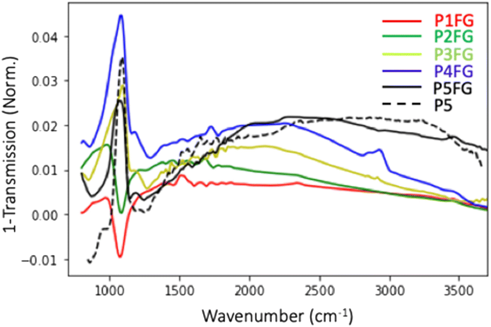 | ||
| Fig. 8 Normalized extinction (i.e., 1-transmission) curves measured for five different P doses with forming gas annealing, and for sample P5 (3 × 10¹⁵ ions per cm2) without FG annealing. | ||
The carrier density in the SiNCs associated with the active dopant concentration was evaluated by combining FTIR measurements coupled with numerical simulations based on the Green dyadic method (GDM) for various implanted P doses.19 The active dopant concentration varies from 1020 cm−3 for the lowest dose to 4 × 1020 cm−3 for the highest dose. The activation rate is defined as the ratio of this active dopant concentration to the total number of P atoms inserted inside the SiNCs as measured by STEM-EDX in this work and plotted in Fig. 4. Fig. 5(d) shows the activation rate as a function of the implanted P atomic concentration (P/Si nominal ratio), which ranges between 3 and 5%. Unlike in bulk Si, where the fraction of active dopants decreases due to dopant cluster formation,12 this activation rate remains almost independent of the implanted dose. This activation rate is much greater than that previously measured on freestanding (∼1 to 0.01%)64 or silica embedded P-doped SiNCs (0.12%) of the same size.65 More importantly, our activation rates are higher than those reported by Zhou et al.15 on freestanding SiNCs (1%) who used the same methodology as this study, coupling FTIR and STEM-EDX measurements. Our values are of the order of magnitude of the ones recently deduced from FTIR measurements on freestanding Si/SiOx core/shell SiNCs elaborated via high temperature annealing in phosphorus vapor that show activation efficiency in the range of 0.8–7%.66 The activation efficiency of our small embedded doped SiNCs is one order of magnitude lower than that we have measured in a previous work on Si nanostructures produced by the top-down processing of hyperdoped Si overlayers. In this case, the activation process was performed in the bulk state by melt laser annealing, allowing active dopant concentrations above 1021 cm−3, close to the best state-of-the-art values.11,12 In Fig. 5(d), we have compared our activation rate in SiNCs to the one measured on bulk Si implanted with the same P/Si ratio as sample P4FG and annealed under the same conditions (1050 °C for 60 s). Surprisingly, both the bulk sample and the doped SiNCs have the same activation rate of 5%. As a result, we can conclude that there is likely no size effect on the activation rate, which is solely dependent on annealing conditions.
Conclusions
We achieved the bottom up synthesis of SiNCs massively doped at the nanoscale and embedded in a silica matrix by combining sequential low energy ion implantation and rapid thermal annealing processes. Doping silica-embedded SiNCs results in a thermodynamically favorable configuration, with P doping impurities incorporated into the NC cores at concentrations up to six times higher than P solid solubility in bulk Si. We proposed a new mechanism to explain the growth of SiNCs at high P doses based on the presence of Si supersaturation in the matrix caused by Si recoiling atoms generated during the P implantation process, which favors the increase of Si diffusivity and feeds the SiNCs. Doping enhances their surface passivation, which can be further improved by FG annealing. We showed that surface defect healing is an important step in the emergence of plasmon resonance, especially for small NCs. Finally, despite introducing P concentrations far above the solubility limit into the SiNC core, activation rates as low as 5% were measured. These values are however comparable to those obtained in bulk Si under the same doping conditions, indicating that the clustering effects, which limit the activation rate at these high doping concentrations, are unaffected at the nanoscale.Author contributions
M. Z.: investigation, funding acquisition, and writing – original draft; J-M. P.: investigation and writing – review and editing; N. C.: investigation and writing – review and editing; H. R.: supervision (A. E. G.), funding acquisition, and writing – review and editing; A. E. G.: investigation; R. D.: investigation; E. T.: supervision (R. D.) and writing – review and editing; F. C.: funding acquisition and writing – review and editing; T. H.: investigation and writing – review and editing; V. P.: conceptualization and writing – review and editing; F. G.: conceptualization, supervision (M. Z. and N. C.), and writing – review and editing; C. B.: conceptualization, funding acquisition, supervision (M. Z. and N. C.), and writing – review and editing.Conflicts of interest
There are no conflicts to declare.Acknowledgements
This work was partly funded by ANR DONNA (ANR-18-CE09-0034). The authors thank the China Scholarship Council (201801810118) for funding. The authors acknowledge Béatrice Pécassou from CEMES-CNRS for Si implantations and Jean-Christophe Marrot and Eric Imbernon from the LAAS-CNRS micro and nanotechnologies platform, a member of the French RENATECH network for phosphorus implantations. The authors thank Nikolay Cherkashin from CEMES-CNRS for the absolute strain measurements.References
- K. Kneipp, Y. Wang, H. Kneipp, L. T. Perelman, I. Itzkan, R. R. Dasari and M. S. Feld, Phys. Rev. Lett., 1997, 78, 1667 CrossRef CAS.
- E. M. Larsson, C. Langhammer, I. Zorić and B. Kasemo, Science, 2009, 326, 1091–1094 CrossRef CAS PubMed.
- V. Dusastre, H. Atwater and A. Polman, Energy, 2010, 9, 1–11 Search PubMed.
- L. Bois, F. Bessueille, F. Chassagneux, Y. Battie, N. Destouches, C. Hubert, A. Boukenter and S. Parola, Colloids Surf., A, 2008, 325, 86–92 CrossRef CAS.
- S. Bakhti, N. Destouches and A. V. Tishchenko, J. Quant. Spectrosc. Radiat. Transfer, 2014, 146, 113–122 CrossRef CAS.
- A. Lalisse, G. Tessier, J. Plain and G. Baffou, J. Phys. Chem. C, 2015, 119, 25518–25528 CrossRef CAS.
- S. Law, V. Podolskiy and D. Wasserman, Nanophotonics, 2013, 2, 103–130 CrossRef CAS.
- J. M. Luther, P. K. Jain, T. Ewers and A. P. Alivisatos, Nat. Mater., 2011, 10, 361–366 CrossRef CAS PubMed.
- G. V. Naik, V. M. Shalaev and A. Boltasseva, Adv. Mater., 2013, 25, 3264–3294 CrossRef CAS PubMed.
- S. Ossicini, E. Degoli, F. Iori, E. Luppi, R. Magri, G. Cantele, F. Trani and D. Ninno, Appl. Phys. Lett., 2005, 87, 173120 CrossRef.
- J.-M. Poumirol, C. Majorel, N. Chery, C. Girard, P. R. Wiecha, N. Mallet, R. Monflier, G. Larrieu, F. Cristiano and A.-S. Royet, et al. , ACS Photonics, 2021, 8, 1393–1399 CrossRef CAS.
- N. Chery, M. Zhang, R. Monflier, N. Mallet, G. Seine, V. Paillard, J. Poumirol, G. Larrieu, A. Royet and S. Kerdilès, et al. , J. Appl. Phys., 2022, 131, 065301 CrossRef CAS.
- D. J. Rowe, J. S. Jeong, K. A. Mkhoyan and U. R. Kortshagen, Nano Lett., 2013, 13, 1317–1322 CrossRef CAS PubMed.
- N. J. Kramer, K. S. Schramke and U. R. Kortshagen, Nano Lett., 2015, 15, 5597–5603 CrossRef CAS PubMed.
- S. Zhou, X. Pi, Z. Ni, Y. Ding, Y. Jiang, C. Jin, C. Delerue, D. Yang and T. Nozaki, ACS Nano, 2015, 9, 378–386 CrossRef CAS PubMed.
- P. Rohani, S. Banerjee, S. Sharifi-Asl, M. Malekzadeh, R. Shahbazian-Yassar, S. J. Billinge and M. T. Swihart, Adv. Funct. Mater., 2019, 29, 1807788 CrossRef.
- S. Milliken, I. T. Cheong, K. Cui and J. G. Veinot, ACS Appl. Nano Mater., 2022, 5, 15785–15796 CrossRef CAS.
- S. Milliken, K. Cui, B. A. Klein, I. T. Cheong, H. Yu, V. K. Michaelis and J. G. Veinot, Nanoscale, 2021, 13, 18281–18292 RSC.
- M. Zhang, J.-M. Poumirol, N. Chery, C. Majorel, R. Demoulin, E. Talbot, H. Rinnert, C. Girard, F. Cristiano and P. R. Wiecha, et al. , Nanophotonics, 2022, 11, 3485–3493 CrossRef CAS.
- M. Carrada, A. Haj Salem, B. Pécassou, R. Carles and G. Ben Assayag, J. Appl. Phys., 2017, 122, 103101 CrossRef.
- R. Demoulin, M. Roussel, S. Duguay, D. Muller, D. Mathiot, P. Pareige and E. Talbot, J. Phys. Chem. C, 2019, 123, 7381–7389 CrossRef CAS.
- M. Perego, G. Seguini, E. Arduca, J. Frascaroli, D. De Salvador, M. Mastromatteo, A. Carnera, G. Nicotra, M. Scuderi and C. Spinella, et al. , Nanoscale, 2015, 7, 14469–14475 RSC.
- C. Bonafos, B. Colombeau, M. Carrada, A. Altibelli and A. Claverie, Mater. Sci. Eng., B, 2002, 88, 112–117 CrossRef.
- A. Claverie, C. Bonafos, G. B. Assayag, S. Schamm, N. Cherkashin, V. Paillard, P. Dimitrakis, E. Kapetenakis, D. Tsoukalas and T. Muller, et al. , Defect Diffus. Forum, 2006, 258, 531–541 Search PubMed.
- S. L. Anderson, E. J. Luber, B. C. Olsen and J. M. Buriak, Chem. Mater., 2016, 28, 5973–5975 CrossRef CAS.
- N. A. Bert, V. V. Chaldyshev, N. A. Cherkashin, V. N. Nevedomskiy, V. V. Preobrazhenskii, M. A. Putyato, B. R. Semyagin, V. I. Ushanov and M. A. Yagovkina, J. Appl. Phys., 2019, 125, 145106 CrossRef.
- M. A. Luong, N. Cherkashin, B. Pécassou, C. Sabbione, F. Mazen and A. Claverie, Nanomaterials, 2021, 11, 1729 CrossRef CAS PubMed.
- B. Cordero, V. Gómez, A. E. Platero-Prats, M. Revés, J. Echeverría, E. Cremades, F. Barragán and S. Alvarez, Dalton Trans., 2008, 2832–2838 RSC.
- L. C. Cousar, Graduate Theses and Dissertations, https://scholarworks.uark.edu/etd/1138, 2015.
- S.-M. Liang and R. Schmid-Fetzer, J. Phase Equilib. Diffus., 2014, 35, 24–35 CrossRef CAS.
- F. Vurpillot, A. Bostel and D. Blavette, Appl. Phys. Lett., 2000, 76, 3127–3129 CrossRef CAS.
- R. Khelifi, D. Mathiot, R. Gupta, D. Muller, M. Roussel and S. Duguay, Appl. Phys. Lett., 2013, 102, 013116 CrossRef.
- K. Nomoto, H. Sugimoto, A. Breen, A. V. Ceguerra, T. Kanno, S. P. Ringer, I. P. Wurfl, G. Conibeer and M. Fujii, J. Phys. Chem. C, 2016, 120, 17845–17852 CrossRef CAS.
- R. Guerra and S. Ossicini, J. Am. Chem. Soc., 2014, 136, 4404–4409 CrossRef CAS PubMed.
- N. Garcia-Castello, S. Illera, J. D. Prades, S. Ossicini, A. Cirera and R. Guerra, Nanoscale, 2015, 7, 12564–12571 RSC.
- H. Gnaser, S. Gutsch, M. Wahl, R. Schiller, M. Kopnarski, D. Hiller and M. Zacharias, J. Appl. Phys., 2014, 115, 034304 CrossRef.
- J. Petropoulos, T. Cristiani, P. Dongmo and J. Zide, Nanotechnology, 2011, 22, 245704 CrossRef CAS PubMed.
- E. Arduca and M. Perego, Mater. Sci. Semicond. Process., 2017, 62, 156–170 CrossRef CAS.
- K. Sakamoto, K. Nishi, F. Ichikawa and S. Ushio, J. Appl. Phys., 1987, 61, 1553–1555 CrossRef CAS.
- F. Trad, A. E. Giba, X. Devaux, M. Stoffel, D. Zhigunov, A. Bouché, S. Geiskopf, R. Demoulin, P. Pareige and E. Talbot, et al. , Nanoscale, 2021, 13, 19617–19625 RSC.
- R. Olesinski, N. Kanani and G. J. Abbaschian, Bull. Alloy Phase Diagr., 1985, 6, 130–133 CrossRef CAS.
- R. M. Burger and R. P. Donovan, Fundamentals of Silicon Integrated Device Technology: Oxidation, Diffusion, and Epitaxy, Prentice-Hall, 1967, vol. 1 Search PubMed.
- L. Nesbit, Appl. Phys. Lett., 1985, 46, 38–40 CrossRef CAS.
- A. M. Agarwal and S. T. Dunham, J. Appl. Phys., 1995, 78, 5313–5319 CrossRef CAS.
- B. Garrido Fernández, M. Lopez, C. Garcıa, A. Pérez-Rodrıguez, J. Morante, C. Bonafos, M. Carrada and A. Claverie, J. Appl. Phys., 2002, 91, 798–807 CrossRef.
- M. Fujii, K. Toshikiyo, Y. Takase, Y. Yamaguchi and S. Hayashi, J. Appl. Phys., 2003, 94, 1990–1995 CrossRef CAS.
- X. Hao, E.-C. Cho, G. Scardera, E. Bellet-Amalric, D. Bellet, Y. Shen, S. Huang, Y. Huang, G. Conibeer and M. A. Green, Thin Solid Films, 2009, 517, 5646–5652 CrossRef CAS.
- T. C.-J. Yang, K. Nomoto, B. Puthen-Veettil, Z. Lin, L. Wu, T. Zhang, X. Jia, G. Conibeer and I. Perez-Wurfl, Mater. Res. Express, 2017, 4, 075004 CrossRef.
- S. Solmi and D. Nobili, J. Appl. Phys., 1998, 83, 2484–2490 CrossRef CAS.
- T. Takahashi, S. Fukatsu, K. M. Itoh, M. Uematsu, A. Fujiwara, H. Kageshima, Y. Takahashi and K. Shiraishi, J. Appl. Phys., 2003, 93, 3674–3676 CrossRef CAS.
- J. F. Ziegler, M. D. Ziegler and J. P. Biersack, Nucl. Instrum. Methods Phys. Res., Sect. B, 2010, 268, 1818–1823 CrossRef CAS.
- B. Garrido, M. Lopez, A. Pérez-Rodrıguez, C. Garcıa, P. Pellegrino, R. Ferré, J. Moreno, J. Morante, C. Bonafos and M. Carrada, et al. , Nucl. Instrum. Methods Phys. Res., Sect. B, 2004, 216, 213–221 CrossRef CAS.
- C. Flytzanis, F. Hache, M. Klein, D. Ricard and P. Roussignol, Progress in optics, Elsevier, 1991, vol. 29, pp. 321–411 Search PubMed.
- G. M. Dalpian and J. R. Chelikowsky, Phys. Rev. Lett., 2006, 96, 226802 CrossRef PubMed.
- X. Pi and C. Delerue, Phys. Rev. Lett., 2013, 111, 177402 CrossRef PubMed.
- S. K. Dhungel, J. Yoo, K. Kim, B. Karunagaran, H. Sunwoo, D. Mangalaraj and J. Yi, Mater. Sci. Semicond. Process., 2004, 7, 427–431 CrossRef CAS.
- L. Pavesi and R. Turan, Silicon nanocrystals: fundamentals, synthesis and applications, John Wiley & Sons, 2010 Search PubMed.
- M. Fujii, A. Mimura, S. Hayashi, Y. Yamamoto and K. Murakami, Phys. Rev. Lett., 2002, 89, 206805 CrossRef PubMed.
- X. Pi, R. Gresback, R. Liptak, S. Campbell and U. Kortshagen, Appl. Phys. Lett., 2008, 92, 123102 CrossRef.
- T. Nakamura, S. Adachi, M. Fujii, K. Miura and S. Yamamoto, Phys. Rev. B: Condens. Matter Mater. Phys., 2012, 85, 045441 CrossRef.
- K. Min, K. Shcheglov, C. Yang, H. A. Atwater, M. Brongersma and A. Polman, Appl. Phys. Lett., 1996, 69, 2033–2035 CrossRef CAS.
- S. Withrow, C. White, A. Meldrum, J. Budai, D. Hembree Jr. and J. Barbour, J. Appl. Phys., 1999, 86, 396–401 CrossRef CAS.
- S. Cheylan and R. Elliman, Appl. Phys. Lett., 2001, 78, 1225–1227 CrossRef CAS.
- R. Gresback, N. J. Kramer, Y. Ding, T. Chen, U. R. Kortshagen and T. Nozaki, ACS Nano, 2014, 8, 5650–5656 CrossRef CAS PubMed.
- S. Gutsch, J. Laube, D. Hiller, W. Bock, M. Wahl, M. Kopnarski, H. Gnaser, B. Puthen-Veettil and M. Zacharias, Appl. Phys. Lett., 2015, 106, 113103 CrossRef.
- S. S. Bubenov, S. G. Dorofeev, A. A. Eliseev, N. N. Kononov, A. V. Garshev, N. E. Mordvinova and O. I. Lebedev, RSC Adv., 2018, 8, 18896–18903 RSC.
Footnote |
| † Electronic supplementary information (ESI) available. See DOI: https://doi.org/10.1039/d3nr00035d |
| This journal is © The Royal Society of Chemistry 2023 |