
Degenerate and non-degenerate all-optical switches using violet phosphorus nanosheets
Yang
Gao
a,
Yueqiu
Hu
a,
Cheng
Ling
a,
Guanghao
Rui
 a,
Jun
He
b and
Bing
Gu
*ac
a,
Jun
He
b and
Bing
Gu
*ac
aAdvanced Photonics Center, Southeast University, Nanjing 210096, China. E-mail: gubing@seu.edu.cn
bSchool of Physics and Electronics, Central South University, Changsha 410012, China
cCollaborative Innovation Center of Light Manipulations and Applications, Shandong Normal University, Jinan 250358, China
First published on 21st February 2023
Abstract
As an allotrope of phosphorus, layered violet phosphorus (VP) has a wide range of applications in electronics, photonics, and optoelectronics. However, its nonlinear optical properties remain to be explored. In this work, we prepare and characterize VP nanosheets (VP Ns), investigate their spatial self-phase modulation (SSPM) effects, and develop them in all-optical switching applications. The ring forming time of SSPM and the third-order nonlinear susceptibility of monolayer VP Ns were found to be about 0.4 s and 10−9 esu, respectively. The mechanism of SSPM formed by coherent light–VP Ns interaction is analyzed. Using the superior coherence electronic nonlinearity of VP Ns, we realize degenerate and non-degenerate all-optical switches based on the SSPM effect. It is demonstrated that the performance of all-optical switching can be controlled by adjusting the intensity of the control beam and/or the wavelength of the signal beam. The results will help us to better design and realize non-degenerate nonlinear photonic devices based on two-dimensional nanomaterials.
1. Introduction
Violet phosphorus (VP), first reported by Hittorf in 1865,1 is another layered semiconductor material with a phosphorus structure.2 Compared with black phosphorus (BP), VP has higher thermal stability, higher carrier mobility, wider adjustable bandgap, and stronger anisotropy.3 These salient properties suggest that VP has broad application prospects in the field of optoelectronics. In the last few years, researchers have prepared VP-related nanomaterials and conducted a lot of investigations on their optoelectronic properties. For examples, Zhang et al.4 reported a high yield synthesis of VP crystals; Zhao et al.5 synthesized VP quantum dots and studied their fluorescence properties; Zhang et al.2 investigated the band alignment of few-layer violet phosphorene; Zhang et al.6 explored the phonon properties of VP single crystals; Zhang et al.7 demonstrated the friction anisotropy of violet phosphorene; and Li et al.8 reported the impurity-induced robust trionic effect in layered VP. It is noteworthy that the nonlinear optical properties of BP have been extensively investigated.9–11 However, for VP, although an allotrope of phosphorus, investigation of its nonlinear optical effect has seldom been reported in the literature.12In general, the spatial self-phase modulation (SSPM) effect refers to the phenomenon where multiple concentric self-diffraction rings appear on the far-field observational screen due to the interaction of an intense laser beam with a nonlinear optical material.13,14 In the past decade, the SSPM effect has been observed in atomically thin two-dimensional (2D) nanomaterials, such as graphene,15 transition metal dichalcogenides,16 topological insulators,17 and other types of nanomaterials.9 Meanwhile, researchers have developed a variety of nonlinear photonic devices based on the superior coherence electronic nonlinearity of 2D nanomaterials, such as all-optical switches,16 all-optical diodes,18 all-optical information converters,19 logic gates,20,21 and nonlinear isolators.22 In these applications of nonlinear photonic devices, all-optical switching performance is undoubtedly the most widely demonstrated.16 In all-optical switching experiments, with the help of the SSPM effect of 2D nanomaterials, the free carriers produced by photons of the strong control beam can diffract photons of the signal beam.16 Although the light–control–light two-color switching has been extensively investigated, there are still some unresolved questions, such as what is the relationship between the ring number of these two beams (i.e., control beam and signal beam) and their wavelengths, and whether the switching time of all-optical switches is related to the wavelengths of these two beams? Therefore, it is necessary to study the performance of non-degenerate all-optical switches in detail for further understanding.
In this work, we prepared VP Ns by an ultrasonic method and investigated their SSPM effects. By analyzing the formation and evolution of the self-diffraction rings, we obtained the nonlinear response time and third-order nonlinear susceptibility χ(3) of VP Ns, and discussed the mechanism of SSPM formed by coherent light–VP Ns interaction. Furthermore, based on the SSPM effect of VP Ns, we demonstrated the degenerate and non-degenerate all-optical switches. We experimentally measured and theoretically analyzed the ring number of the signal beam and the switching time of non-degenerate all-optical switches under different signal beam wavelengths. The presented results are helpful for us to better design and realize non-degenerate nonlinear photonic devices based on 2D nanomaterials.
2. Experiments
2.1 Preparation of VP Ns
All samples were prepared by an ultrasonic method, which is a widely used traditional method for preparing 2D materials. The ultrasonic method belongs to the liquid phase stripping method, which is a top-down method.23 The raw material was VP crystals provided by Jiangsu Xianfeng Nanomaterials Technology Co., Ltd. To investigate the influence of solvents on the nonlinear optical response of VP Ns, we chose three different solvents in the layered VP synthesis, namely, 1-methyl-2-pyrrolidone (NMP), N,N dimethylformamide (DMF), and anhydrous C6H2O. This is mainly due to the following two considerations: (i) VP Ns are highly soluble in these three solvents; and (ii) the solvent polarity decreases in the order of NMP > DMF > C2H6O. In the preparation process, the mixed solution of 2 mg of massive VP and 20 ml of solvent was subjected to ultrasonic treatment. During the ultrasonic treatment, attention was paid to keep the temperature below 30 °C to prevent oxidation of VP. Approximately homogenized VP Ns were prepared by centrifugation and purification. The layered VP overcomes the van der Waals force between layers in the liquid phase and then peels off to form nanosheets.2.2 Characterization
The morphology, size, morphological characteristics and crystallographic properties, crystal structure, characteristic structure, and linear optical property of the as-synthesized VP Ns were characterized by atomic force microscopy (AFM), transmission electron microscopy (TEM), selected area electron diffraction (SAED), X-ray diffraction (XRD), Raman spectroscopy, and UV-vis linear absorption spectroscopy, respectively.2.3 Nonlinear optical measurements
It is well-established that the SSPM is extensively adopted to investigate the nonlinear optical effect of various 2D nanomaterials due to its simple experimental method and intuitive results.15 In our experiments, a TEM00 Gaussian laser beam at a wavelength of 532 nm was focused by a convex lens with a focal length of 250 mm, and the beam waist at the focus was estimated to be 56.4 μm. VP Ns dispersed in the three different solvents were respectively placed in 10 mm-thick quartz cuvettes for the SSPM measurements. The back surface of the cuvette was positioned 40 mm before the focus. A white screen placed 160 mm from the back surface of the cuvette was used to detect the far-field self-diffraction intensity pattern.3. Results and discussion
3.1 Characterization results
Fig. 1(a) shows the AFM image of VP Ns, while the inset shows the height profile along the white line. Fig. 1(b) shows the TEM image of VP Ns. The results indicate that the massive VP has been successfully separated into a nanosheet shape by the ultrasonic method. Moreover, the thickness of VP Ns was found to be ∼1.9 nm, which corresponds to the thickness of a single-layer VP nanosheet. The lateral size of VP Ns confirmed by TEM is a few hundred nanometers. The diffraction ring pattern shown in Fig. 1(c) is the SAED result of VP Ns. In situ analysis of morphology and crystallographic properties confirmed that VP Ns are polycrystalline.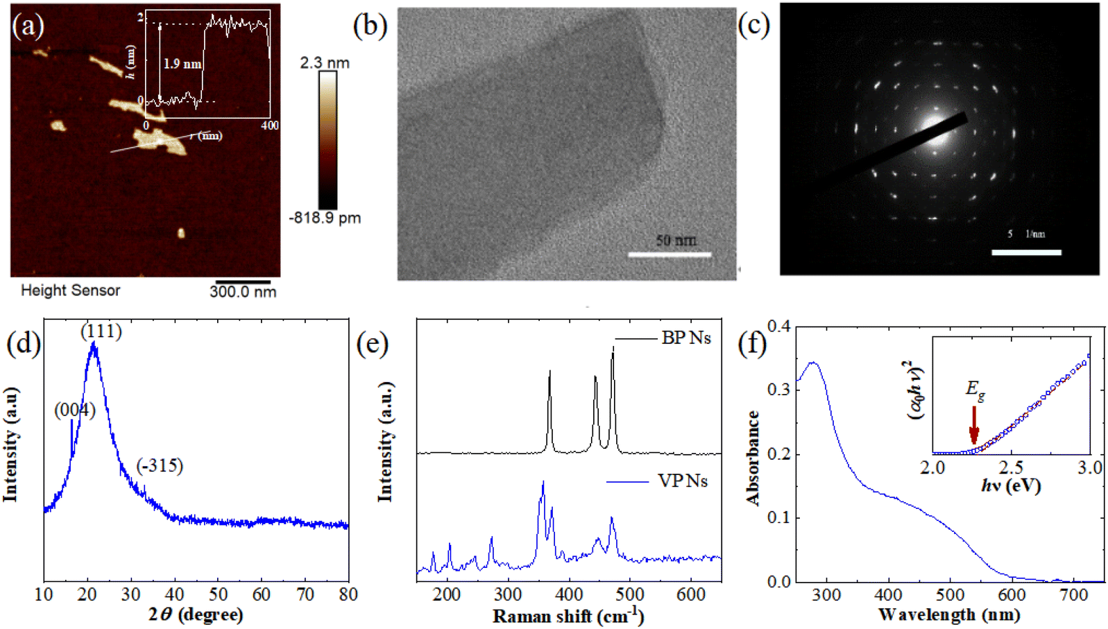 | ||
| Fig. 1 Characterization of VP Ns. (a) AFM image of VP Ns and the height profile along the white line. (b) TEM image of VP Ns. (c) SAED image and (d) XRD pattern of VP Ns. (e) Raman spectra of VP and BP Ns. (f) UV-vis absorption spectrum of VP Ns in NMP solution; the inset is (α0hν)2versus photon energy hν. | ||
The XRD pattern of VP Ns shown in Fig. 1(d) is analyzed as follows: (i) the XRD peaks of VP at 2θ = 16.3° and 33.1° respectively correspond to the (004) and (−315) crystal planes of the VP monoclinic system (specific reference PDF #75-0577); and (ii) the XRD peak at 2θ = 21.7° corresponds to the (111) crystal plane of the VP orthorhombic system (specific reference PDF #72-1161). It is clearly shown that VP Ns are polycrystalline in the monoclinic and orthorhombic forms.
The Raman spectrum mainly reflects the characteristic structure of molecules, which can be used to distinguish VP Ns from BP Ns. Fig. 1(e) shows the Raman spectrum of VP Ns, which has multiple characteristic peaks in the range of 150–300 cm−1 and 350–500 cm−1. This observation is consistent with the result reported recently.24 According to bond distortion, the Raman spectrum of VP Ns shown in Fig. 1(e) can be divided into a high region (350–500 cm−1), a middle region (175–350 cm−1), and a low region (<175 cm−1). The characteristic peaks of these three regions are mainly caused by the stretching and bending, angular deformation, and rotational deformation of the VP layers, respectively. For comparison, the Raman spectrum of BP Ns is also shown by the black line in Fig. 1(e).11 Obviously, the Raman spectra of VP and BP are different. This is because BP is a single crystal with an orthorhombic structure, whereas VP is polycrystalline composed of monoclinic and orthorhombic structures.
Fig. 1(f) shows the UV-vis absorption spectrum of VP Ns in NMP solution. It is shown that the absorption band of VP Ns ranges from ultraviolet to visible light, so its linear absorption coefficient gradually decreases with an increase of wavelength. The bandgap of VP Ns is extrapolated to be Eg = 2.27 eV by Tauc's formulae (α0hν)2 = const(hν − Eg),25 where α0 is the linear absorption coefficient and hν is the incident photon energy. The relationship between (α0hν)2 and hν is shown as the inset in Fig. 1(f). The measured Eg of VP Ns is in good agreement with a recently reported one.26 It is noteworthy that the bandgap of VP Ns is larger than that of few-layer BP Ns with values of 0.3–2 eV.27
3.2 Nonlinear optical properties
In order to obtain an excellent SSPM effect, we examine the dependence of far-field self-diffraction intensity patterns on the conditions, including the types of solvents and the ultrasonic time for preparing VP Ns. We first prepared VP Ns dispersed in NMP, DMF, and C2H6O when the ultrasonic time T = 400 min. The complete ring patterns of three samples at the same intensity are recorded when the number of rings in each case reaches the maximum. For example, Fig. 2(a) shows three complete ring patterns with VP Ns dispersed in NMP, DMF, and C2H6O at I = 31.7 W cm−2. It is found that the number of rings N = 7, 6, and 5 in NMP, DMF, and C2H6O, respectively. Fig. 2(b) presents the intensity dependence of the number of rings for VP Ns dispersed in three different solvents. Since a VP nanosheet is a polar material, the polar solvent is more conducive to the dispersion of VP Ns. It should be noted that the polarity of the solvent decreases in the order of NMP > DMF > C2H6O. Therefore, the dispersity of VP Ns in NMP is better than that in DMF and C2H6O, exhibiting relatively more diffraction rings at the same intensity as shown in Fig. 2(a). This observation can be understood as follows. Compared with DMF and C2H6O, NMP has the strongest polarity, the highest viscosity, and better thermal and chemical stability. During the sonication process, more VP Ns are dispersed in NMP, which increases the concentration of VP Ns, allowing more VP Ns to produce ac electron coherence,15 which leads to an increase in the number of diffraction rings. This concentration-dependent SSPM behavior has recently been confirmed theoretically and experimentally.28 In addition, after three dispersions were kept for 48 hours, it was found that VP Ns were most stable in NMP, while precipitation occurred in DMF and C2H6O. In short, it is optimal to use NMP as the reaction solvent for preparing VP Ns.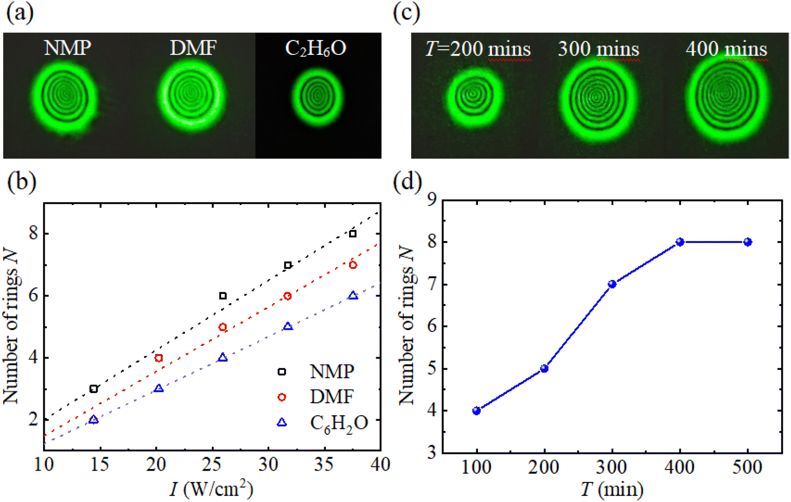 | ||
| Fig. 2 (a) Complete ring patterns with VP Ns dispersed in three different solvents at I = 31.7 W cm−2. (b) Intensity dependence of the number of rings for VP Ns dispersed in three different solvents. (c) Complete ring patterns for VP Ns dispersed in NMP at I = 37.5 W cm−2 with three ultrasonic times T. (d) T-Dependence of the number of rings for VP Ns dispersed in NMP at I = 37.5 W cm−2. | ||
Next, we prepared VP nanosheet dispersions in NMP at different ultrasonic times. Fig. 2(c) shows the complete ring patterns at I = 37.5 W cm−2 for three ultrasonic times T when the number of rings in each case reaches the maximum. It is found that the number of rings N = 5, 7, and 8 when T = 200, 300, and 400 min, respectively. Fig. 2(d) shows the measured N as a function of ultrasonic time T at I = 37.5 W cm−2 for VP Ns dispersed in NMP. Obviously, the number of rings N increases approximately linearly with an increase of ultrasonic time T. However, when T = 400 min, the number of rings tends to be constant and saturation occurs. The results indicate that the best ultrasonic time for preparing VP Ns dispersed in NMP solvent under our experimental conditions is 400 min. In the subsequent work, we only focus on the samples that are VP nanosheet dispersions in NMP prepared with T = 400 min.
It is very necessary to obtain both the nonlinear response time and third-order nonlinear susceptibility χ(3) of VP Ns before using them in developing nonlinear photonic device applications. In the SSPM experiments, we observe the formation process of self-diffraction ring patterns. As an example, Fig. 3(a) presents the self-diffraction ring patterns of the VP nanosheet dispersion in NMP recorded at different times t with I = 37.5 W cm−2. The results show that the radius of self-diffraction rings gradually increases from t = 0 s until t = 0.37 s. At the same time, the number of rings progressively increases from N = 0 to the maximum value of N = 8. Here we define the ring forming time τF as the time when the number of self-diffraction rings reaches the maximum value. Theoretically, the ring forming time is directly related to the thickness h and size R of the nanosheet and the light intensity I according to the relationship τF ∝ R/(Ih).15 After t = 0.37 s, the upper half of the rings starts to collapse due to the thermal convection effect.29,30 At t = 1.73 s, the distorted self-diffraction ring pattern is approximately stable. Fig. 3(b) shows the evolution of the number of rings over time t at three different intensities. It can be seen that the number of self-diffraction rings increases nonlinearly and tends to be saturated with an increase of time t. Such evolution behavior can be described as N(t) = N0[1 − exp(−t/τ)], where N0 and τ are the number of rings and the formation time when forming the complete ring pattern, respectively. The best fitting N–t shown in Fig. 3(b) gives τ = 0.19, 0.20, and 0.19 s at I = 25.9, 31.7, and 37.5 W cm−2, respectively. On the other hand, the ring forming times were found to be τF = 0.46, 0.41, and 0.37 s at I = 25.9, 31.7, and 37.5 W cm−2, respectively. The obtained τF value is inversely proportional to the light intensity I, which is consistent with the observations reported previously.16,21,28 The measured τF value of VP Ns is slightly shorter than the τF of ∼0.7 s of BP Ns.9
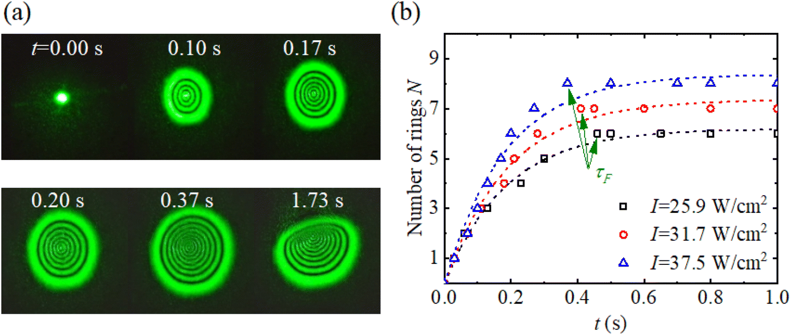 | ||
| Fig. 3 (a) The self-diffraction ring patterns of VP nanosheet dispersion in NMP recorded at different times t with I = 37.5 W cm−2. (b) The evolution of the number of rings N over time t at three different intensities. | ||
It is known to all that the nonlinear refractive index n2 of the material can be directly inferred from the intensity dependence of the ring number in the complete ring pattern.14 The nonlinear refractive index n2 can be obtained by:15
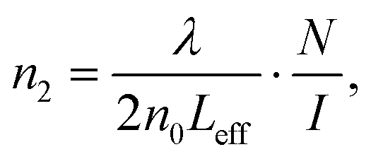 | (1) |
Since the obtained n2 comes from the contribution of multilayer nanosheets in the dispersion, it is more significant to calculate the third-order nonlinear susceptibility χ(3) of monolayer nanosheets. The third-order nonlinear susceptibility χ(3)monolayer of monolayer VP Ns can be evaluated by the following formula:15
 | (2) |
 , where Ttotal and Tmonolayer are the linear transmittances of VP dispersions and a VP monolayer, respectively. From the measured Ttotal = 38% at 532 nm, we estimate Neff ∼ 322, by taking the typical value of Tmonolayer ∼ 99.7%.31–33 Accordingly, the third-order nonlinear susceptibility of monolayer VP Ns is obtained to be χ(3)monolayer = (3.4 ± 0.3) × 10−9 esu at 532 nm, which is comparable with those of BP Ns,9,34 NbSe2 Ns,35 and boron Ns.20 Note that χ(3)monolayer is correlated to the carrier mobility μ by the empirical formula χ(3)monolayer = 0.146 × √μ.36 With the measured χ(3)monolayer value, the carrier mobility of single-layer VP is estimated to be μ = 0.54 × 103 cm2 V−1 s−1, which is close to the calculated value in the b direction.37 Very recently this correlation between χ(3)monolayer and μ has been proved to be still valid in hole-based materials.38
The mechanism of SSPM formed by coherent light–VP Ns interaction is illustrated in Fig. 4. As shown in the inset of Fig. 1(f), the bandgap of VP Ns was found to be Eg = 2.27 eV. The incident photon energy in our experiments is hν = 2.33 eV (i.e., λ = 532 nm), which falls in the conical region of the VP nanosheet band structure, as shown in Fig. 4(a). This means that the electrons in the valence band could absorb photons and transition to the conduction band. Under intense light irradiation, these photons can excite electrons to produce the coherent nonlinear Kerr effect. It is worth noting that when the photon energy is less than the bandgap of the VP Ns (e.g., hv = 1.85 eV at 671 nm, hv = 1.59 eV at 780 nm, and hv = 1.17 eV at 1064 nm), the photons cannot excite the coherent nonlinear Kerr effect. This is why we did not observe the SSPM effect with the laser beams at 671 nm, 780 nm, and 1064 nm in the experiment. When the intense Gaussian beam (its intensity distribution is shown in Fig. 4(b)) passes through VP Ns suspended in NMP, many random VP Ns turn into wind-chime sheets under the action of the laser field.16 As illustrated in Fig. 4(c), the nonlocal ac electron coherence between different nanosheet domains of 2D-nanomaterials leads to the alignment and reorientation of VP Ns,16 producing an additional phase shift Δφ caused by the coherent electronic nonlinearity. On the schematic diagram of nonlinear phase shift Δφ shown in Fig. 4(c), the light diffracted at A and B has the same wave vector and propagates to P on the far-field observational screen. If the phase difference between A to P and B to P is an odd or even multiple of π, destructive or constructive interference takes place, respectively. Since the light–VP Ns interaction maintains circular symmetry, as shown in Fig. 4(d), the SSPM effect gives rise to the appearance of a far-field self-diffraction intensity pattern with a concentric ring structure.
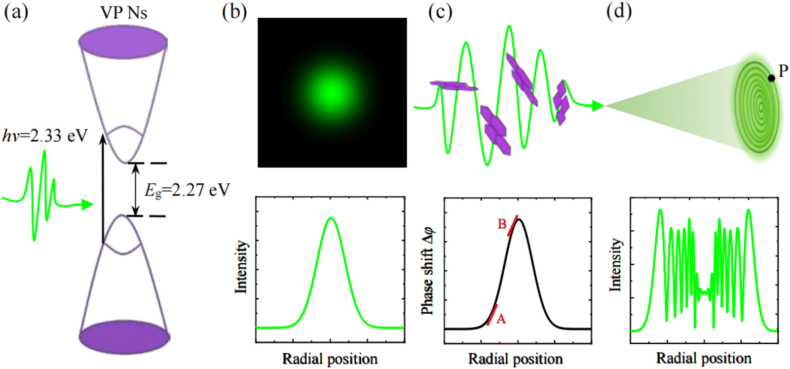 | ||
| Fig. 4 SSPM formation mechanism of light–VP Ns interaction based on the wind-chime model. (a) Schematic diagram of the bandgap structure of VP Ns. (b) Intensity pattern and intensity profile of the incident laser beam. (c) Photoinduced reorientation of VP Ns and the schematic profile of nonlinear phase shift Δφ induced by the coherent electronic nonlinearity.16 (d) Far-field self-diffraction ring pattern originating from the coherent light–VP Ns interaction. | ||
4. All-optical switch applications
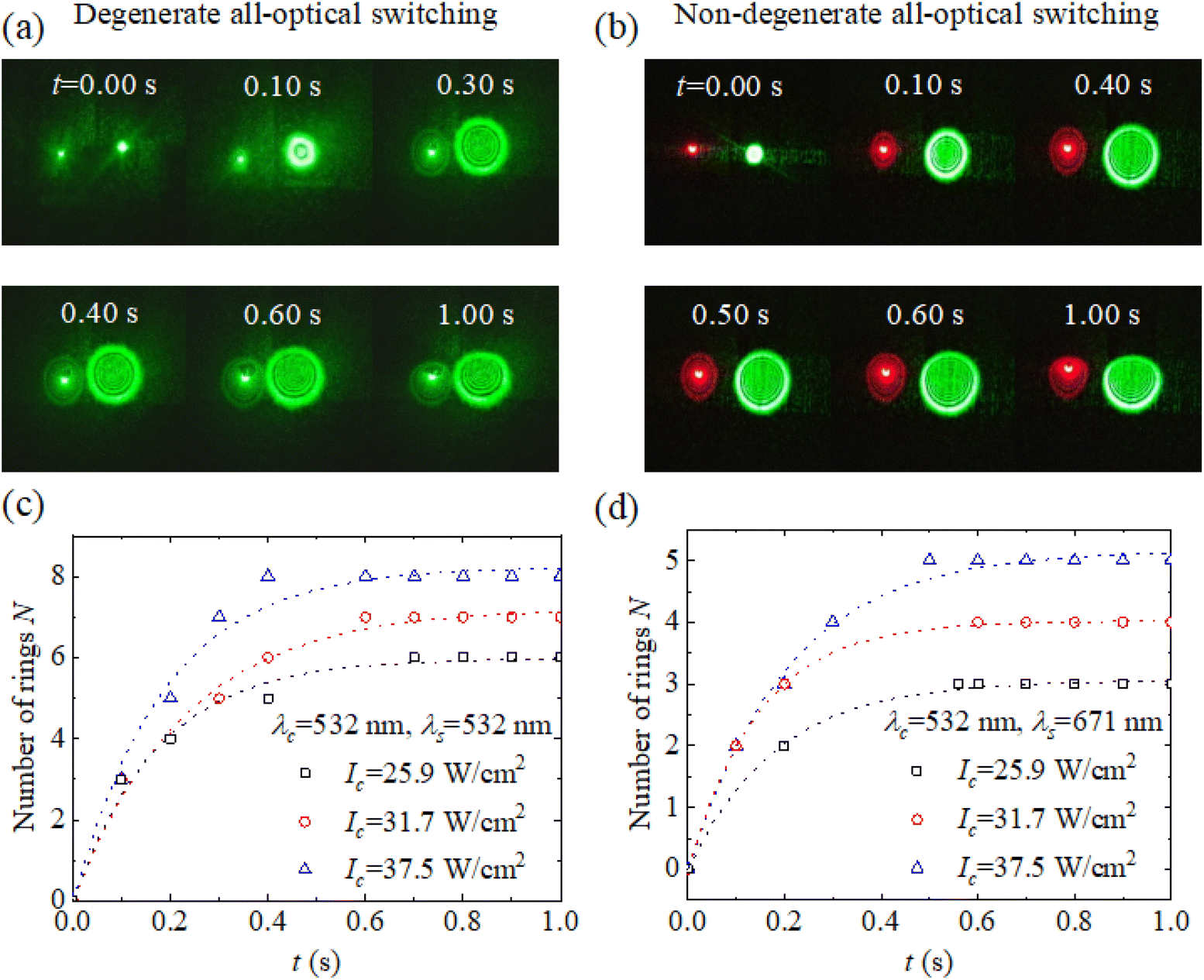
Using the superior coherence electronic nonlinearity of VP Ns, we design an all-optical switch based on the SSPM effect.16 The principle of this all-optical switch based on SSPM in VP Ns is as follows: under the irradiation of a strong control beam, ac electron coherence appears in VP Ns, and then the free carriers produced by photons of the control beam diffract photons of the signal beam.The experimental configuration of the all-optical switch is shown in Fig. 5(a). The intensity of the strong control beam at 532 nm is adjusted by a λ/2 waveplate and a Glan–Taylor (G–T) prism. Then, the strong control beam and the weak signal beam are focused by the convex lens, respectively. Two focused beams overlapping in the focal region pass through a quartz cuvette containing VP nanosheet dispersions. The control beam and the signal beam excite the SSPM effect in the VP dispersions. As a result, the self-diffraction ring patterns of both the control beam and the signal beam can be observed on the white screen placed in the far field. According to whether the wavelengths of the control beam and the signal beam are the same, the performance of degenerate and non-degenerate all-optical switches can be demonstrated as shown in Fig. 5(a). In the degenerate all-optical switch experiment, the wavelengths of both the control beam and the signal beam are 532 nm. In the non-degenerate all-optical switch experiment, the wavelength of the signal beam can be 671, 780, or 1064 nm, which is different from that of the control beam at 532 nm.
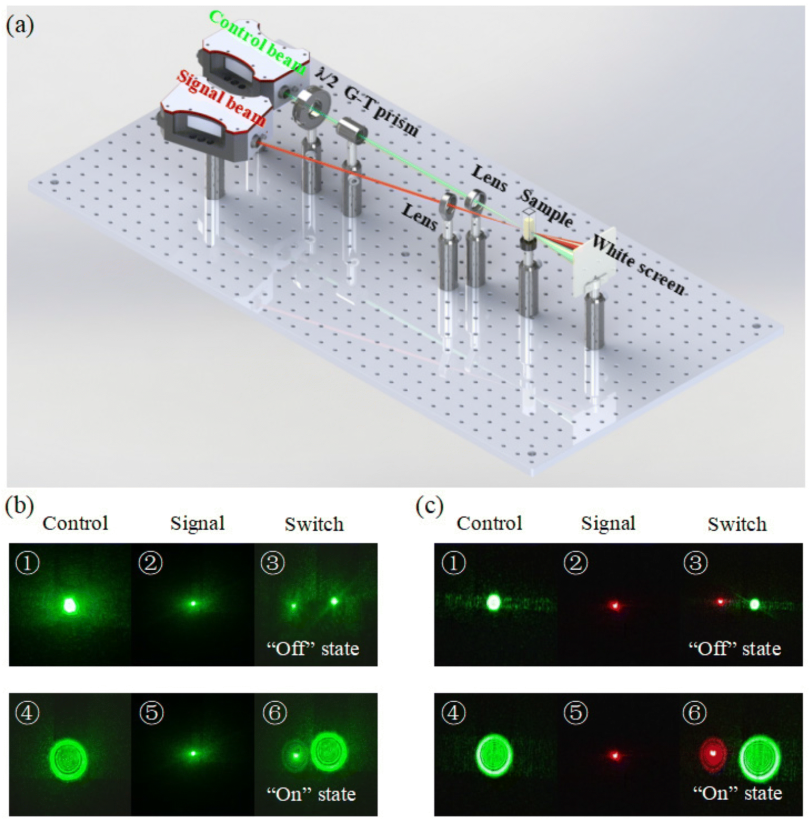 | ||
| Fig. 5 (a) The experimental configuration for the all-optical switch. (b) Degenerate (532–control–532) and (c) non-degenerate (532–control–671) all-optical switching performances in VP nanosheet dispersions. | ||
With the help of the experimental configurations shown in Fig. 5(a), for instance, Fig. 5(b) and (c) demonstrate the degenerate (532–control–532) and non-degenerate (532–control–671) all-optical switching performances in VP nanosheet dispersions, respectively. At first, we adjust the intensity of the control beam (λc = 532 nm) to Ic = 5.0 W cm−2, which is lower than the threshold value of Ith = 8.6 W cm−2 for exciting the SSPM effect, and the intensity of the signal beam (λs = 532 nm or λs = 671 nm) always remains Is = 0.9 W cm−2. At this time, the intensities of the two beams are too low to excite the self-diffraction ring pattern. As demonstrated in the first columns of Fig. 5(b) and (c), both degenerate and non-degenerate all-optical switches are in the “off” state. Now, we increase the intensity of the control beam to Ic = 37.5 W cm−2, which exceeds the threshold value Ith, while maintaining the intensity of the signal beam unchanged. At this moment, the control beam independently excites the SSPM effect of VP Ns, whereas the signal beam cannot. When the control and signal beams act on VP nanosheet dispersions simultaneously, the green–green (532 nm, 532 nm) or green–red (532 nm, 671 nm) self-diffraction ring pattern appears on the white screen. The results show that the control beam modulates the signal beam via the SSPM effect in VP Ns, and both beams excite the self-diffraction rings. As shown in the second columns of Fig. 5(b) and (c), the green (532 nm) and red (671 nm) signal beams are fully excited, and the degenerate and non-degenerate all-optical switches are in the “on” state, respectively.
Similar to the VP N SSPM effect excited by a single beam, as shown in Fig. 3(a), the dynamic evolution of the VP N SSPM excited by both control and signal beams also includes the formation of two self-diffraction rings. For instance, Fig. 6(a) and (b) show self-diffraction ring patterns recorded at different times with Ic = 37.5 W cm−2 for λs = 532 nm and 671 nm, respectively. The experimental observations show that both the control and signal beams evolve from a spot to a complete diffraction ring as time t goes by. Under our experimental conditions, it is found that the ring formation processes of both the control beam and the signal beam are almost synchronous for degenerate all-optical switching. For non-degenerate all-optical switching, however, the ring formation process of the long-wavelength signal beam is slightly behind that of the control beam. Fig. 6(c) and (d) show the evolutions of ring number of the signal beam at 532 nm and 671 nm over time under three different intensities Ic, respectively. These results are similar to the ring number evolution of SSPM in VP Ns shown in Fig. 3(b). Interestingly, under the same intensity of the 532 nm control beam, it is shown that the ring number of the 532 nm signal beam is significantly higher than that of the 671 nm signal beam.
 | ||
| Fig. 6 Formation processes of (first column) degenerate and (second column) non-degenerate all-optical switching based on SSPM in VP Ns. Dynamic processes of light–control–light modulations with Ic = 37.5 W cm−2 for the signal beams at (a) 532 nm and (b) 671 nm. The evolutions of ring number of signal beams at (c) 532 nm and (d) 671 nm over time t under three different intensities Ic. | ||
Now we focus on the number of complete rings formed by both the control and signal beams with the help of SSPM in VP Ns. In the experiments, the intensity of the strong control beam Ic is gradually increased while the intensity of the weak signal beam remains unchanged. Fig. 7(a) shows the Ic-dependent ring number N of the 532 nm control beam and the 532 nm, 671 nm, 780 nm, or 1064 nm signal beam. As the intensity of the control beam increases from Ic = 14.4 W cm−2 to 37.5 W cm−2, the number of self-diffraction rings excited by both the control beam and the signal beam increases approximately linearly. Interestingly, in the degenerate case, the number of two-diffraction rings increases synchronously. In the non-degenerate case, however, the number of diffraction rings excited by the control beam is significantly higher than that of the signal beam (see Fig. 7(a)).
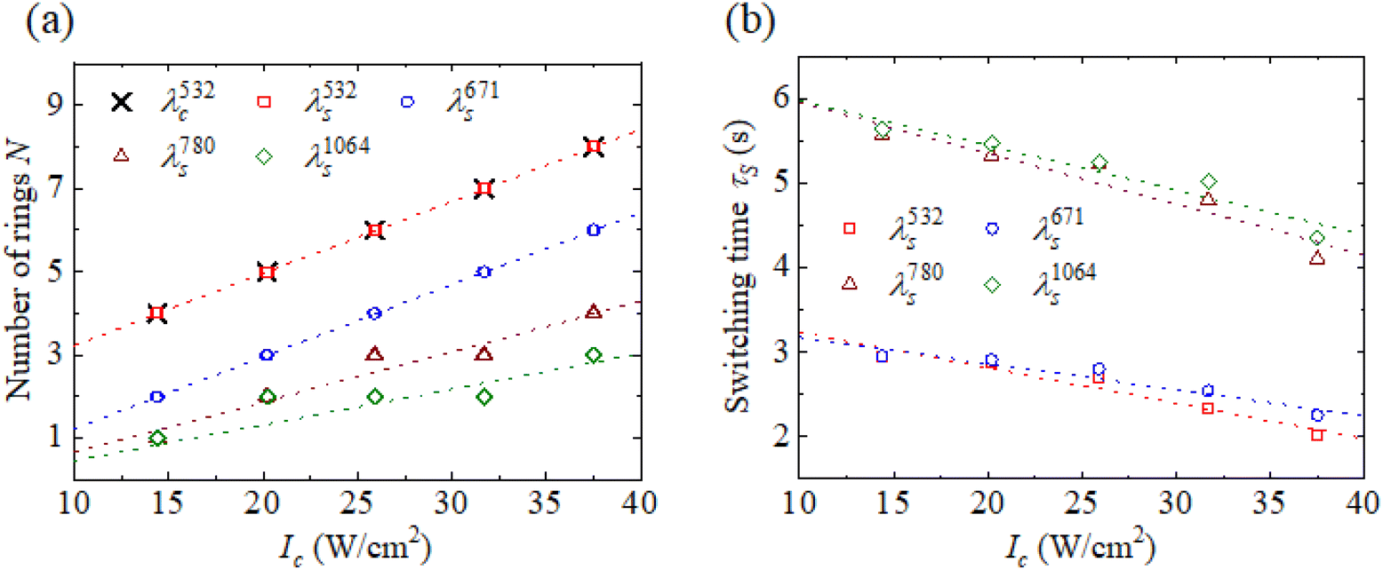 | ||
| Fig. 7 I c-Dependent (a) ring number N and (b) switching time τS for the signal beams at 532 nm, 671 nm, 780 nm, and 1064 nm with the control beam at 532 nm. The dotted lines are for visual guidance. | ||
The wavelength-dependent ring number observed in the light–control–light modulation experiment can be explained by SSPM in VP Ns. For the control and signal beams with Gaussian spatial distribution, the ring numbers excited by the control and signal beams can be respectively written as:15
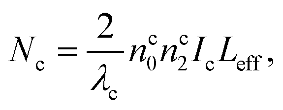 | (3) |
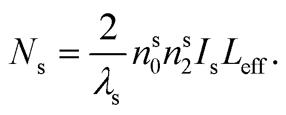 | (4) |
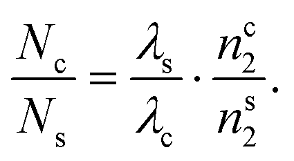 | (5) |
Eqn (5) gives the ratio of the ring numbers induced by the control and signal beams. When the wavelengths of the control and signal beams degenerate, i.e., λc = λs, eqn (5) is reduced to Nc/Ns = 1. The prediction result of this situation is consistent with the experimental observation (see Fig. 7(a)). For the non-degenerate light–control–light modulation, we approximately simplify eqn (5) to Nc/Ns = λs/λc. Theoretically, we calculate Nc532/Ns671 = 1.26, Nc532/Ns780 = 1.47, and Nc532/Ns1064 = 2. For comparison, we experimentally measure Nc532/Ns671 = 1.33, Nc532/Ns780 = 2.00, and Nc532/Ns1064 = 2.67 at Ic = 37.5 W cm−2. Obviously, when the wavelength difference between the control beam and the signal beam is relatively small, the theoretical predictions are in good agreement with the experimental results. However, when the wavelength difference between the control beam and the signal beam is relatively large, the difference between nc2 and ns2 cannot be ignored, resulting in significant differences between the simplified theory of Nc/Ns = λs/λc and experimental results.
To quantitatively evaluate the response time of the all-optical switches, we define the switching time τS, that is, the time period from the control beam acting on VP Ns to the signal beam forming a stable distorted self-diffraction ring pattern with the help of the SSPM effect. Fig. 7(b) shows the Ic-dependent switching time τS for the all-optical switches with the 532 nm control beam and the 532 nm, 671 nm, 780 nm, or 1064 nm signal beam. It is found that the switching time τS for the degenerate and non-degenerate all-optical switches becomes shorter with an increase of Ic, which is similar to the evolution of the SSPM ring shown in Fig. 3(b). This phenomenon can be understood as follows: the greater the intensity of the control beam, the stronger the optical nonlinearity in VP Ns, and the faster the dynamic formation of the self-diffraction ring. Most previous studies only focused on the influence of the intensity of the control beam on the all-optical switching time.16,33 In fact, the wavelength of the signal beam is also closely related to the all-optical switching performance. As shown in Fig. 7(b), for a fixed Ic, the switching time for the non-degenerate all-optical switches increases with the wavelength of the signal beam. This is because of the fact that the greater the wavelength difference between the control beam and the signal beam, the lower the SSPM efficiency in VP Ns, and the slower the evolution of the self-diffraction ring of the signal beam. In short, the switching time of the non-degenerate all-optical switch can be controlled by adjusting the intensity of the control beam and/or the wavelength of the signal beam.
5. Conclusion
In summary, we have prepared VP Ns by an ultrasonic method and characterized them by means of AFM, SAED, XRD, Raman, and UV-vis absorption analyses. By performing the SSPM experiments at 532 nm under different intensities, we have determined that the ring forming time of VP Ns dispersed in NMP is about 0.4 s and the third-order nonlinear susceptibility of monolayer VP Ns is about 10−9 esu. We have analyzed the mechanism of SSPM formed by coherent light–VP Ns interaction and confirmed that the SSPM effect mainly originates from the coherent electronic nonlinearity of VP Ns. In particular, we have designed and realized degenerate and non-degenerate all-optical switches based on the SSPM effect of VP Ns. It is shown that the ratio of the ring number of the control beam and the signal beam is inversely proportional to the ratio of their wavelengths in the light–control–light process, and the switching time of the all-optical switch can be controlled by adjusting the intensity of the control beam and/or the wavelength of the signal beam. These results will help us to better design and realize non-degenerate nonlinear photonic devices based on 2D nanomaterials, such as all-optical switches, all-optical modulators, and all-optical information converters.Conflicts of interest
There are no conflicts to declare.Acknowledgements
This work was supported by the National Nature Science Foundation of China (Grant Nos. 12074066, 12274074). Y. Gao acknowledges the support by Postgraduate Research & Practice Innovation Program of Jiangsu Province (Grant No: KYCX21_0086).References
- W. Hittorf, Ann. Phys., 1865, 202, 193 CrossRef.
- B. Zhang, Z. Wang, H. Huang, L. Zhang, M. Gu, Y. Cheng, K. Wu, J. Zhou and J. Zhang, J. Mater. Chem. A, 2020, 8, 8586–8592 RSC.
- G. Schusteritsch, M. Uhrin and C. J. Pickard, Nano Lett., 2016, 16, 2975–2980 CrossRef CAS PubMed.
- L. Zhang, M. Gu, L. Li, X. Zhao, C. Fu, T. Liu, X. Xu, Y. Cheng and J. Zhang, Chem. Mater., 2020, 32, 7363–7369 CrossRef CAS.
- R. Zhao, S. Liu, X. Zhao, M. Gu, Y. Zhang, M. Jin, Y. Wang, Y. Cheng and J. Zhang, J. Mater. Chem. A, 2022, 10, 245–250 RSC.
- L. Zhang, H. Huang, Z. Lv, L. Li, M. Gu, X. Zhao, B. Zhang, Y. Cheng and J. Zhang, ACS Appl. Electron. Mater., 2021, 3, 1043–1049 CrossRef CAS.
- B. Zhang, L. Zhang, C. Chen, M. Gu, Y. Cheng and J. Zhang, 2D Mater., 2022, 9, 025002 CrossRef.
- Y. Li, S. Cai, W. Lai, C. Wang, L. Rogée, L. Zhuang, L. Zhai, S. Lin, M. Li and S. Lau, Adv. Opt. Mater., 2022, 10, 2101538 CrossRef CAS.
- J. Zhang, X. Yu, W. Han, B. Lv, X. Li, S. Xiao, Y. Gao and J. He, Opt. Lett., 2016, 41, 1704–1707 CrossRef CAS PubMed.
- L. Miao, B. Shi, J. Yi, Y. Jiang, C. Zhao and S. Wen, Sci. Rep., 2017, 7, 3352 CrossRef PubMed.
- Y. Gao, Y. Hu, G. Rui, J. He, Y. Cui and B. Gu, Optik, 2022, 259, 168969 CrossRef CAS.
- L. Zhou, J. Kang, Y. Dong, Y. Wang, Y. Li, H. Huang, S. Xiao, Y. Wang and J. He, Nano Res. DOI:10.1007/s12274-022-5224-3.
- W. R. Callen, B. G. Huth and R. H. Pantell, Appl. Phys. Lett., 1967, 11, 103–105 CrossRef.
- S. D. Durbin, S. M. Arakelian and Y. R. Shen, Opt. Lett., 1981, 6, 411–413 CrossRef CAS PubMed.
- R. Wu, Y. Zhang, S. Yan, F. Bian, W. Wang, X. Bai, X. Lu, J. Zhao and E. Wang, Nano Lett., 2011, 11, 5159–5164 CrossRef CAS PubMed.
- Y. Wu, Q. Wu, F. Sun, C. Cheng, S. Meng and J. Zhao, Proc. Natl. Acad. Sci. U. S. A., 2015, 112, 11800–11805 CrossRef CAS PubMed.
- B. Shi, L. Miao, Q. Wang, J. Du, P. Tang, J. Liu, C. Zhao and S. Wen, Appl. Phys. Lett., 2015, 107, 151101 CrossRef.
- Y. Shan, Z. Li, B. Ruan, J. Zhu, Y. Xiang and X. Dai, Nanophotonics, 2019, 8, 2225–2234 CAS.
- Y. Jia, Z. Li, M. Saeed, J. Tang, H. Cai and Y. Xiang, Opt. Express, 2019, 27, 20857–20873 CrossRef CAS PubMed.
- C. Song, Y. Liao, Y. Xiang and X. Dai, Sci. Bull., 2020, 65, 1030–1038 CrossRef CAS PubMed.
- K. Sk, B. Das, N. Chakraborty, M. Samanta, S. Bera, A. Bera, D. S. Roy, S. K. Pradhan, K. K. Chattopadhyay and M. Mondal, Adv. Opt. Mater., 2022, 10, 200791 Search PubMed.
- L. Wu, Y. Zhang, X. Yuan, F. Zhang, W. Huang, D. Ma, J. Zhao, Y. Wang, Y. Ge, H. Huang, N. Xu, J. Kang, Y. Xiang, Y. Zhang, J. Li and H. Zhang, Appl. Mater. Today, 2020, 19, 100589 CrossRef.
- S. Lin, W. Lai, Y. Li, W. Lu, G. Bai and S. Lau, SmartMat, 2021, 2, 226–233 CrossRef CAS.
- A. Fali, M. Snure and Y. Abate, Appl. Phys. Lett., 2021, 118, 163105 CrossRef CAS.
- J. Tauc, R. Grigorovici and A. Vancu, Phys. Status Solidi, 1966, 15, 627–637 CrossRef CAS.
- A. G. Ricciardulli, Y. Wang, S. Yang and P. Samorì, J. Am. Chem. Soc., 2022, 144, 3660–3666 CrossRef CAS PubMed.
- J. Qiao, X. Kong, Z. Hu, F. Yang and W. Ji, Nat. Commun., 2014, 5, 4475 CrossRef CAS PubMed.
- Y. He, J. Zhang, S. Xiao, Y. Wang and J. He, Chin. Opt. Lett., 2022, 20, 011901 CrossRef.
- W. Ji, W. Chen, S. Lim, J. Lin and Z. Guo, Opt. Express, 2006, 14, 8958–8966 CrossRef CAS PubMed.
- R. Karimzadeh, J. Opt., 2012, 14, 095701 CrossRef.
- S. Dey, A. Govindaraj, K. Biswas and C. N. R. Rao, Chem. Phys. Lett., 2014, 595–596, 203–208 CrossRef CAS.
- Z. Guo, H. Zhang, S. Lu, Z. Wang, S. Tang, J. Shao, Z. Sun, H. Xie, H. Wang, X. Yu and P. K. Chu, Adv. Funct. Mater., 2015, 25, 6996–7002 CrossRef CAS.
- P. Manivasagan, S. W. Jun, V. T. Nguyen, N. T. P. Truong, G. Hoang, S. Mondal, M. S. Moorthy, H. Kim, T. T. V. Phan, V. H. M. Doan, C. Kim and J. Oh, J. Mater. Chem. B, 2019, 7, 3811–3825 RSC.
- Y. Shi, Y. Gao, Y. Hu, Y. Xue, G. Rui, L. Ye and B. Gu, Opt. Lasers Eng., 2022, 158, 107168 CrossRef.
- Y. Jia, Y. Liao, L. Wu, Y. Shan, X. Dai, H. Cai, Y. Xiang and D. Fan, Nanoscale, 2019, 11, 4515–4522 RSC.
- L. Hu, F. Sun, H. Zhao and J. Zhao, Opt. Lett., 2019, 44, 5214–5217 CrossRef CAS PubMed.
- Y. Xu, Q. Long, D. Li and P. Li, Phys. Chem. Chem. Phys., 2022, 24, 3379–3385 RSC.
- Y. Huang, H. Zhao, Z. Li, L. Hu, Y. Wu, F. Sun, S. Meng and J. Zhao, Adv. Mater., 2023, 2208362 CrossRef PubMed.
| This journal is © The Royal Society of Chemistry 2023 |