DOI:
10.1039/D2NR07107J
(Paper)
Nanoscale, 2023,
15, 7745-7754
Transfer-printing-enabled GeSn flexible resonant-cavity-enhanced photodetectors with strain-amplified mid-infrared optical responses†
Received
19th December 2022
, Accepted 22nd March 2023
First published on 25th March 2023
Abstract
Mid-infrared (MIR) flexible photodetectors (FPDs) constitute an essential element for wearable applications, including health-care monitoring and biomedical detection. Compared with organic materials, inorganic semiconductors are promising candidates for FPDs owing to their superior performance as well as optoelectronic properties. Herein, for the first time, we present the use of transfer-printing techniques to enable a cost-effective, nontoxic GeSn MIR resonant-cavity-enhanced FPDs (RCE-FPDs) with strain-amplified optical responses. A narrow bandgap nontoxic GeSn nanomembrane was employed as the active layer, which was grown on a silicon-on-insulator substrate and then transfer-printed onto a polyethylene terephthalate (PET) substrate, eliminating the unwanted defects and residual compressive strain, to yield the MIR RCE-FPDs. In addition, a vertical cavity was created for the GeSn active layer to enhance the optical responsivity. Under bending conditions, significant tensile strain up to 0.274% was introduced into the GeSn active layer to effectively modulate the band structure, extend the photodetection in the MIR region, and substantially enhance the optical responsivity to 0.292 A W−1 at λ = 1770 nm, corresponding to an enhancement of 323% compared with the device under flat conditions. Moreover, theoretical simulations were performed to confirm the strain effect on the device performance. The results demonstrated high-performance, nontoxic MIR RCE-FPDs for applications in flexible photodetection.
Introduction
Flexible optoelectronic devices operating in the mid-infrared (MIR) region—generally defined in the spectral range of 1.8–5 μm1—have received considerable attention for use in a wide range of emerging applications such as gas sensing, strain sensing, optical links, environment monitoring, health diagnosis, and wearable photonic textiles.2–4 Among the various components required for flexible optoelectronic systems, photodetectors (PDs) are crucial for optical – electric conversion. Although flexible PDs (FPDs) composed of organic or 2D materials operating in the MIR region have been extensively explored,5–8 they typically suffer from low quantum efficiency resulting from weak absorption and poor reliability. Meanwhile, semiconductor-based FPDs are being extensively used owing to their unique advantages of superior quantum efficiency.9–12 To achieve efficient MIR photodetection, narrow-bandgap semiconductors are necessary. Currently, compound semiconductors based on III–V materials such as InAs and InSb that are dominating the market satisfy this requirement, and FPDs based on III–V materials have been demonstrated as well.12 However, the toxicity and wafer cost hinder the practical applications.
Moreover, FPDs based on group-IV semiconductors are being explored for MIR photodetection, because they are nontoxic, environment-friendly, and affordable, thereby rendering them more suitable for wearable applications. Although the applicability of Si13,14 and Ge15–17 PDs has been demonstrated, their application to MIR photodetection is difficult owing to the cut-off wavelength of 1.1 and 1.5 μm, respectively. To extend the photodetection range to the MIR region, tensile strain can be employed using various approaches such as thermal expansion gradient between Si and Ge18,19 and stressors;20 however, a limited amount of tensile strain can be incorporated which creates challenges. Another promising approach is alloying Ge with Sn, which is another group-IV element.21,22 With the addition of Sn into Ge, the direct bandgap can be effectively reduced, thereby enabling efficient absorption in the MIR region.23–25 Moreover, the presence of L-conduction band in GeSn alloys generates a unique momentum – space carrier separation scheme,25,26 which facilitates high-performance MIR photodetection. Recent theoretical studies have reported that the performance of GeSn PDs is comparable, and can be even superior to that of the current commercially available semiconductor MIR PDs,24,25 which make it a promising candidate for low-cost practical applications. Despite the limited solubility of Sn in Ge of ∼1%,27,28 the recent advancements in low-temperature growth techniques using molecular beam epitaxy (MBE),27,28 chemical vapor deposition (CVD),29–31 and sputter32 have enabled the growth of high-quality GeSn layers on Si or silicon-on-insulator (SOI) substrates, which can yield Sn contents up to 36%.30 Various GeSn-based PDs have been demonstrated with an extended photodetection range,33–48 attaining up to 3.7 μm47 and enhanced quantum efficiency, which highlights their potential for efficient MIR photodetection. However, the epitaxy of GeSn layers on Si or SOI substrates typically requires an appropriate buffer (usually Ge) to improve the material quality and induces an indispensable biaxial compressive strain.35 This unfavorable biaxial compressive strain significantly increases the bandgap energies and weakens the effectiveness of Sn-alloying, thereby hindering the performance of GeSn-based PDs.23,48 A few approaches have been proposed to eliminate biaxial compressive strain, such as suspended structures,49 graded GeSn buffer technologies,40 and wafer-binding technologies,50 and an extended photodetection range up to 4.6 μm has been experimentally achieved.49 However, as these GeSn PDs are fabricated on rigid substrates, they lack the flexibility required for wearable applications.
To the best of our knowledge, this study demonstrates the first strain-free GeSn MIR resonant-cavity-enhanced FPDs (RCE-FPDs), wherein the performance is further enhanced under bending conditions. In particular, single-crystal GeSn nanomembranes (NMs) were grown on an SOI substrate using low-temperature MBE and subsequently transferred on to flexible polyethylene terephthalate (PET) substrates. The transfer was performed using a transfer-printing technique with a mechanically strong SU8 adhesion layer to eliminate unwanted defective region and residual compressive strain. Thus, a device with improved performance was realized. After the transfer, GeSn active layer sandwiched between a low-refractive-index (RI) SU8 layer and air creates a vertical cavity enabling a multiple-pass reflection scheme, which enhances the light–matter interaction under resonance conditions and significantly augments the optical responsivity. Notably, if the GeSn RCE-FPDs are subjected to bending conditions, a tensile strain up to 0.274% can be introduced into the GeSn active layer. This tensile strain can effectively modulate the band structure, extend the photodetection range, and significantly enhance the absorption in the MIR region. Furthermore, the strain effect on the device performance was theoretically analyzed to support the experimental findings. The results demonstrate the feasibility of GeSn RCE-FPDs with enhanced optical responses, establishing a new avenue for high-performance, nontoxic, sensitive, reliable, and flexible MIR photodetectors for versatile wearable applications.
Analysis of impact of strain on band structure of GeSn alloys
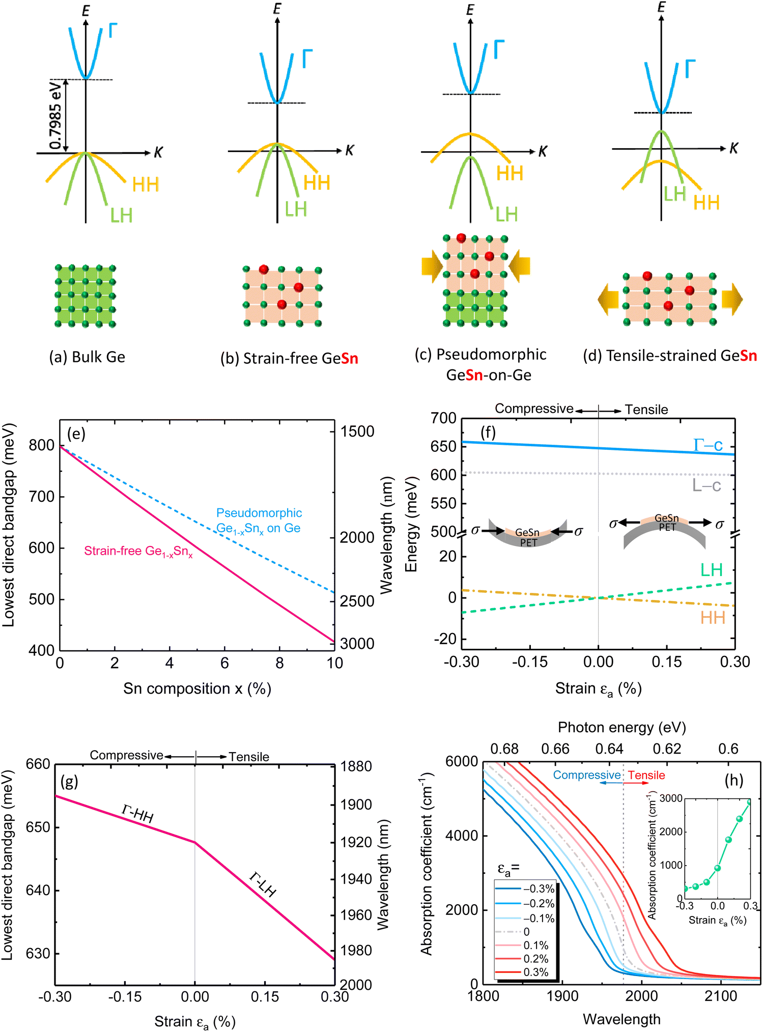
For FPDs, a strain can be induced under the bending condition, which will significantly impact the device performance. We first systematically investigated the impact of strain on the electronic band structure, optical absorption, and device performance of GeSn PDs. The direct bandgap of bulk Ge is 0.7985 eV at T = 300 K (Fig. 1(a)). By adding Sn into Ge, the electronic band structure can be effectively modified (Fig. 1(b)). As a result, the direct-gap absorption edge can be red-shifted to extend the photodetection range and enhance the quantum efficiency of GeSn PDs. Currently, a suitable buffer (typically Ge) is used to facilitate the growth of GeSn on Si substrates and improve the material quality. However, as shown in Fig. 1(c), the growth of Ge1−xSnx layer on Ge buffer within a critical thickness is pseudomorphic,35 leading to a significant in-plane biaxial compressive strain of 0.143x owing to the larger lattice constant of GeSn than Ge. This compressive strain lifts the direct conduction band and shifts the heavy-hole (HH) band above the light-hole (LH) band. As a result, the lowest direct-gap transition takes place between the HH band and Γ-valley conduction band, which increases with increasing compressive strain. Fig. 1(e) shows the calculated lowest direct-gap transition energy for bulk GeSn and pseudomorphic GeSn-on-Ge as a function of Sn content. Evidently, the compressive strain can significantly increase the lowest direct-gap transition energy, equivalently reducing the “effective Sn content” in the GeSn active layer. Thus, it is essential to eliminate the unwanted compressive strain to achieve strain-free GeSn alloys and “recover” the performance of GeSn PDs. Furthermore, the performance of GeSn PDs can be further enhanced by introducing tensile strain/stress to modify the energy band (Fig. 1(d)). Here we investigate the band structure of GeSn subjected to a uniaxial stress (σ) along 〈100〉 direction induced by bending, as shown in the inset in Fig. 1(f). The resulting strain fields can be expressed as| | 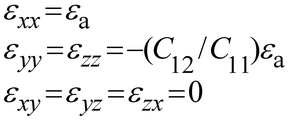 | (1) |
where C11 and C12 denote the elements of stiffness matrix of GeSn, which were obtained through the linear interpolation between those of Ge and Sn.22εa represents the normal strain along 〈100〉 direction. The band structure was evaluated using a multiple-band k·p method, considering the band nonparabolicity effect23,51 and the strain-induced energy shifts were modeled using the deformation potential theory.51 Thereafter, the absorption coefficient was calculated using Fermi's golden rule.51 The parameters used in the simulations were obtained from ref. 22. The composition-dependent bandgap energies of bulk GeSn were evaluated using22| | | Eg(Ge1−xSnx) = xEg(Ge) + (1 − x)Eg(Sn) − bx(1 − x) | (2) |
where Eg(Ge) = 0.7985 eV and Eg(Sn) = −0.413 eV denote the direct bandgap energies of Ge and α-Sn, respectively, and b = 2.89 eV denotes the bowing parameter for GeSn alloys at T = 300 K.23,35 The calculated band edges and the lowest direct bandgap of the GeSn layer formulated as a function of uniaxial strain are presented in Fig. 1(f) and (g), respectively. With the application of the compressive strain (i.e., under bend-up conditions), the Γ-conduction band shifted to a higher energy. Moreover, for the valence band, the HH shifted above the LH band (Fig. 1(f)). Consequently, the lowest direct bandgap was defined as the transition energy from the HH band and the Γ-conduction band (HH → cΓ), which increased with the increasing compressive strain, as shown in Fig. 1(g). By contrast, with the application of the tensile strain (i.e., under bend-down conditions), the Γ-conduction band shifted to a lower energy, whereas the LH band shifted above the HH band (Fig. 1(f)). Thus, the lowest direct bandgap can be defined as the optical transition from the LH band to the Γ-conduction band (LH → cΓ), and it decreased with the increasing tensile strain (Fig. 1(g)). The calculated direct-gap absorption coefficient spectra of the GeSn active layer with various uniaxial strains are shown in Fig. 1(h). Without strain, the absorption coefficient decreased with the increasing wavelength and becomes negligible at the direct bandgap. With the application of the compressive strain, the lowest bandgap significantly increased, thereby blue-shifting the direct-gap absorption edge. Thus, the absorption coefficient reduced as it is proportional to the joint density-of-state (JDOS; for bulk materials, the JDOS is proportional to 
![[thin space (1/6-em)]](https://www.rsc.org/images/entities/char_2009.gif) 51). By contrast, the application of the tensile strain reduces the direct bandgap, thereby red-shifting the absorption spectrum, increasing the JDOS, and significantly enhancing the absorption coefficient. The calculated absorption coefficient at λ = 1977 nm is depicted as a function of uniaxial strain in the inset of Fig. 1(h). The absorption coefficient is enhanced by a factor of 301% for the increase in strain from 0% to 0.274%, thereby enhancing the quantum efficiency of the PDs.
51). By contrast, the application of the tensile strain reduces the direct bandgap, thereby red-shifting the absorption spectrum, increasing the JDOS, and significantly enhancing the absorption coefficient. The calculated absorption coefficient at λ = 1977 nm is depicted as a function of uniaxial strain in the inset of Fig. 1(h). The absorption coefficient is enhanced by a factor of 301% for the increase in strain from 0% to 0.274%, thereby enhancing the quantum efficiency of the PDs.
 |
| | Fig. 1 Schematic of electronic band structures: (a) bulk Ge, (b) strain-free GeSn, (c) pseudomorphic GeSn on Ge, and (d) tensile-strained GeSn. (e) Calculated lowest direct bandgap energy as a function of Sn content for pseudomorphic GeSn-on-Ge and strain-free GeSn. (f) Calculated various band edges of Ge0.957Sn0.043 active layer as a function of uniaxial strain induced by bending. Energy zero is set to the valence band maximum of unstrained GeSn. (g) Calculated lowest direct bandgap of Ge0.957Sn0.043 active layer as a function of uniaxial strain. (h) Calculated absorption coefficient spectra of Ge0.957Sn0.043 active layer with varying uniaxial strain values. Vertical dashed line represents calculated direct bandgap of unstrained GeSn active layer. Inset: Calculated absorption coefficient at λ = 1977 nm as a function of unaxial strain. | |
Material growth and device fabrication
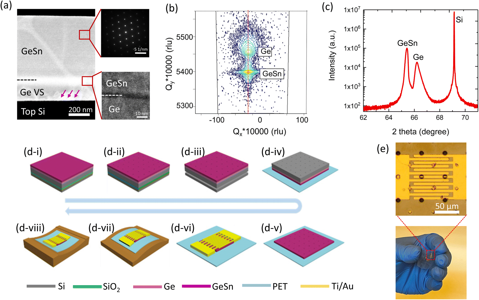
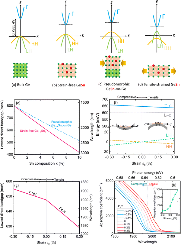
The fabrication of the GeSn RCE-FPD involves the growth and fabrication of the material. In this study, the sample was prepared using low-temperature MBE on an SOI substrate with a 2.5 μm-thick top Si layer and a 1 μm-thick buried oxide (BOX) layer under a base pressure less than 5 × 10⁻¹¹ torr. The epitaxy started with the growth of a strain-relaxed Ge virtual substrate (VS) using a two-step growth technique: (a) a 100 nm-thick Si buffer layer grown at 600 °C, (b) a 100 nm-thick Si buffer layer grown at 350 °C, (c) a 60 nm-thick Ge seed layer grown at 350 °C followed by in situ thermal annealing at 800 °C for 5 min, and (d) a 60 nm-thick Ge layer grown at 550 °C. To suppress Sn segregation, the growth temperature was reduced to 150 °C to grow a 370 nm-thick intrinsic GeSn layer. The structure was capped with a 3 nm-thick Si layer. Note that although the intrinsic GeSn layer was updoped, a background p-type doping concentration of 6.5 × 1016 cm−3 was detected by Hall measurements. The cross-sectional transmission electron microscopy (XTEM) image of the grown sample is illustrated in Fig. 2(a), wherein significant misfit dislocations that distinguish the interface between the Ge and top Si layer were observed. However, they were absent in the GeSn active layer. By contrast, a sharp and flat interface was observed between the Ge VS and GeSn active layer, as shown in the lower inset of Fig. 2(a). A selected electron diffraction of the GeSn active layer, as shown in the higher inset of Fig. 2(a), confirmed the single-crystalline nature and desired quality of the grown sample material. Additionally, X-ray diffraction (XRD) techniques were employed to probe the structural properties of the grown sample. The X-ray reciprocal space mapping (XRDRSM) of symmetrical (004) plane is presented in Fig. 2(b), which portrays two distinguished peaks that can be ascribed to the Ge and GeSn layers, respectively. Note that the two peaks were vertically aligned with the same Qx value, implying that the GeSn layer was pseudomorphic to the underlying Ge VS. The high-resolution ω–2θ scan of the grown sample is presented in Fig. 2(c), from which the Bragg's angles of the Ge and GeSn layers were extracted to determine their lattice constants along the growth direction. According to the analysis procedure described in ref. 41, the GeSn layer had Sn content of 4.3% and an in-plane biaxial compressive strain of 0.52%.
 |
| | Fig. 2 (a) Cross-sectional transmission electron microscopy image of the grown sample. The insets show the FFT pattern of the selected region in the GeSn layer and the high-resolution image of the GeSn/Ge interface. (b) X-ray reciprocal space mapping around symmetric (004) plane and (c) ω–2θ scan of the grown sample. (d) Schematic of fabrication process of our strain-free GeSn RCE-FPDs: (d-i) growth of 370 nm-thick GeSn on an SOI substrate via MBE, (d-ii) patterning of etching hole array, (d-iii) releasing GeSn/Ge/Si NM by removal of sacrificial SiO2 layer in HF solution, (d-iv) flip-transfer GeSn/Ge/Si on SU8 2002-coated PET substrates, (d-v) removal of top Si template and Ge buffer layer using RIE, (d-vi) patterning and deposition of interdigitated metal electrodes, and (d-vii, d-viii) bending down and up to apply mechanical strain. (e) Optical image of our fabricated GeSn RCE-FPDs. | |
The procedure for fabricating the GeSn RCE-FPDs is illustrated in Fig. 2(d). The process initiated with an epitaxial growth of 370 nm-thick GeSn on a SOI with a Ge VS using MBE (Fig. 2(d-i)). Subsequently, the photoresist was first spin coated to protect the GeSn layer and for lithography. An array of holes with a diameter of 3 μm and a spacing of 50 μm were patterned with standard optical lithography and etched down to expose the sacrificial layer (BOX layer) by reactive ion etching (RIE) (Fig. 2(d-ii)). Thereafter, the samples were placed in 49% hydrofluoric acid (HF) solution for 30 min to release the GeSn/Ge/Si NMs by removing the sacrificial layer (Fig. 2(d-iii)). The released GeSn/Ge/Si NMs were flip transferred on SU8 2002-coated PET substrate with a thickness of 175 μm (Fig. 2(d-iv)). Subsequently, the top Si and Ge layers on the GeSn were etched away using RIE to alleviate the unwanted residual compressive strain caused by material growth and achieve strain-free GeSn NMs (Fig. 2(d-v)). Further, to remove the defective region in the GeSn layer and improve the device performance, the GeSn layer was over-etched, and the final thickness of GeSn NMs was estimated as 240 nm. Eventually, Ti/Au (10/80 nm) interdigitated pads (length: 100 μm; width and pitch: 4 μm) were deposited using an e-beam evaporator to complete the fabrication of the devices (Fig. 2(d-vi)). An optical image of the fabricated GeSn RCE-FPD is displayed in Fig. 2(e), which evidently demonstrates the flexibility of the device. Thereafter, the devices were conformally attached along 〈100〉 direction with extreme precautions on the convex (Fig. 2(d-vii)) and concave (Fig. 2(d-viii)) bending fixtures with a radius of R to introduce uniaxial stress under bend-up and bend-down conditions, respectively. For comparison, a GeSn reference PD was fabricated using the as-grown GeSn on the SOI substrate with the same device structure (labelled as GeSn-on-SOI device).
Electrical characterization
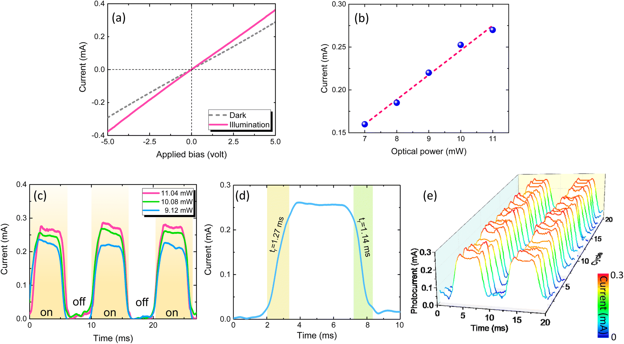
The current–voltage characteristics of the fabricated GeSn RCE-FPDs under flat conditions in a dark environment and illumination with a 1503 nm laser—measured at room temperature using a sourcemeter (Keithley 2400)—are presented in Fig. 3(a). Under the dark environment, the dark current (Idark) indicated a linear relationship with the applied bias voltage, displaying appropriate Ohmic contact for the devices. In addition, the Idark–V characteristics exhibited a symmetric behavior in the forward- and reverse-bias region owing to the symmetrical metal pads design. Under illumination using a laser with a wavelength of 1503 nm and power of 1.4 mW, the significant increase in the current evidently confirmed the photodetection ability of the fabricated GeSn RCE-FPDs. Fig. 3(b) shows the measured current at 6 V bias voltage of the fabricated GeSn RCE-FPDs under flat condition illuminated with λ = 1900 nm broadband light source (ASE 1900, Thorlabs) with various optical powers. It is not difficult to see that the current increases linearly with increasing optical power. Fitting the data with a linear function yields a slope of 28.7 mA W−1, which represents the responsivity of our GeSn RCE-FPDs. In addition, a linear correction coefficient of R2 = 0.986 was obtained, highlighting good linearity of the photocurrent for our GeSn RCE-FPDs. Fig. 3(c) presents the time responses of the fabricated GeSn RCE-FPDs under flat condition illuminated with λ = 1900 nm broadband light source for different optical powers optically chopped at 100 Hz. Under illumination, the photoresponses were recorded with clear on/off switching behavior with a good on/off ratio of ∼40. It is noted that the obtained on/off ratio is lower than the typical values of 102–105 for 2D-material-based MIR PDs52,53 and ∼108 for InGaAs/InP p–i–n FPD,12 mainly attributed to the relatively high dark current of the metal–semiconductor–metal PD structure.54 By suppressing the dark current, it is possible to further enhance the on/off ratio to improve the device performance. With increased optical power, the photocurrent increased accordingly. Fig. 3(d) shows the time response of the GeSn RCE-FPD upon switching on/off with the rising time (tr) and falling time (tf), which denote the time required for the phococurrent to increase from 10% to 90% of the maximum and decreases from 90% to 10% of the maximum photocurrent, respectively. Our GeSn RCE-FPDs exhibited short rising time and falling times of tr = 1.27 ms and tf = 1.14 ms, respectively. The fast response time is desirable for flexible and wearable devices. The response time of metal–semiconductor–metal PDs is mainly limited by the transit time of photogenerated carriers which related to the interelectrode spacing.55 Note that high-speed GeSn PDs with a bandwidth of 30 GHz has been experimentally demonstrated.56 Thus, it is anticipated that further optimization of our GeSn RCE-FPDs could significantly improve the response time to achieve high-speed operation.57,58Fig. 3(e) shows the switching on/off response of the GeSn RCE-FPDs for 20 cycles measured using a 1900 nm, 10 ± 0.5 mW light source optically chopped at 100 Hz. Upon repetitive cycles of MIR light illumination, our GeSn RCE-FPDs exhibited repeatable photocurrent and time response, suggesting excellent reliability. These results validate the ability of the MIR photodetection of the fabricated GeSn RCE-FPDs.
 |
| | Fig. 3 (a) Current–voltage characteristics of the GeSn RCE-FPDs under flat conditions in a dark environment and during light illumination with a 1503 nm, 1.4 mW laser. (b) Measured current as a function of incident optical powers. (c) Time response of fabricated GeSn device at 6 V bias with illumination using 1900 nm broadband light source for various optical powers. (d) Rising time and falling time of the RCE-FPDs under flat conditions upon switching on/off using 1900 nm broadband light source with a power of 10.08 mW. (e) Time response of the GeSn RCE-FPDs at 6 V bias under flat conditions upon switching on/off for 20 cycles using 1900 nm broadband light source with a power of 10 ± 0.5 mW. | |
Optical characterization
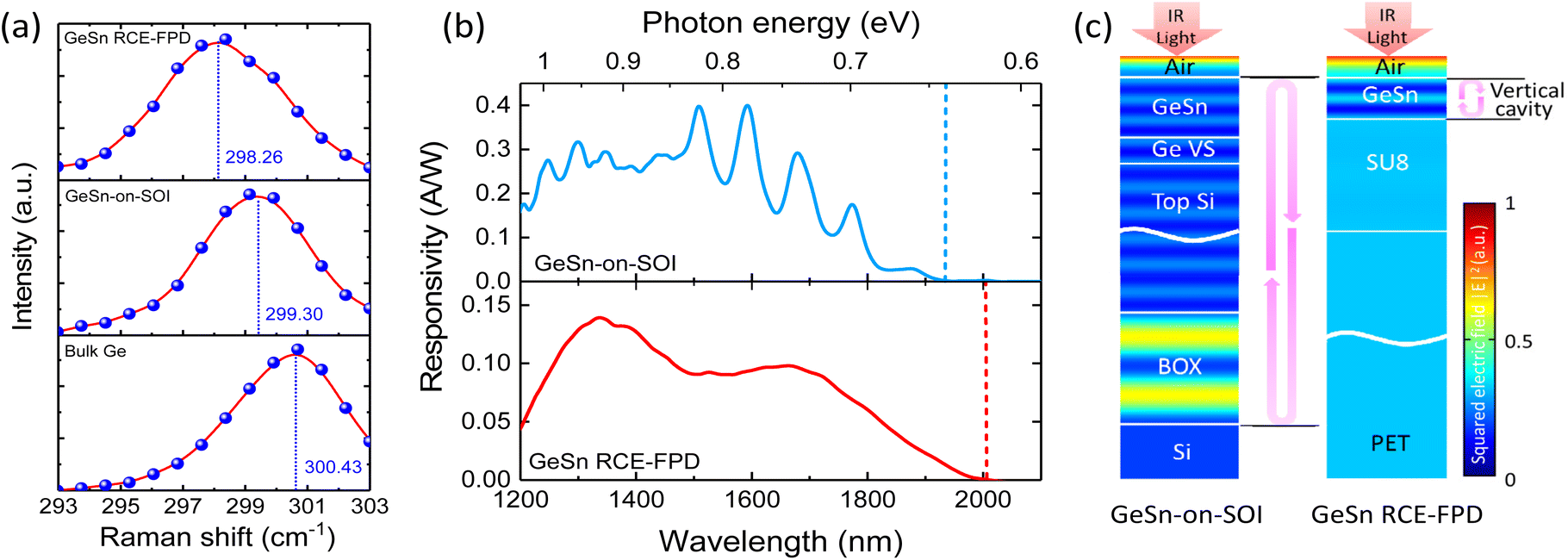
First, we compared the optical properties of the GeSn RCE-FPD and GeSn-on-SOI PD. Raman analysis was performed to characterize the strain status of the samples using a Raman microscopy (UHT S300 & WITEC) with a 532 nm excitation laser under backscattering scheme. The laser light was focused on the sample surface using an objective of 100× and a spot size of ∼1 μm. The measured Raman spectra of the bulk Ge, as-grown GeSn-on-SOI, and flexible GeSn RCE-FPD under flat conditions are presented in Fig. 4(a). After fitting the experimental data using Gaussian functions, the peak positions were determined. For bulk Ge, the Raman peak corresponding to the longitudinal phonon–phonon mode appeared at 300.43 cm−1. For the GeSn-on-SOI, the Raman peak shifted to 299.30 cm−1. This shift was attributed to the introduction of Sn into the material. For the GeSn RCE-FPD under flat conditions, the peak further shifted to 298.26 cm−1. The Raman shift is related to strain via the expression Δω = k × ε, where the strain-shift coefficient for GeSn is k = −181 cm−1 from ref. 59. Thus, the shift of Raman peak to a lower wavenumber is an indication of relaxation of the compressive strain in the GeSn layer.
 |
| | Fig. 4 (a) Raman spectra of GeSn RCE-FPDs under flat conditions, GeSn-on-SOI, and bulk Ge, revealing strain relaxation in GeSn RCE-FPDs. (b) Optical responsivity spectra of the reference GeSn-on-Si PD and the GeSn RCE-FPDs under flat condition. Vertical dashed lines represent cut-off wavelength. (c) Simulated optical field distributions of GeSn RCE-FPDs and GeSn-on-SOI PDs. | |
The optical responsivity of the devices was measured using a tunable light source comprising a 250 W quartz tungsten halogen (QTH) lamp and a 25 cm monochromator. After the emitted light was optically chopped at 200 Hz, it was incident normally on the device using an objective of 50×. A sourcemeter (Keithley 2400) was used to provide voltage to the device in series with a load resistance of 50 Ω. The voltage drop across the load resistance was accurately recorded using a lock-in amplifier (SRS, SR830) to determine the photocurrent. A lock-in technique was adopted to enhance the signal-to-noise ratio. The incident optical power on the device was measured using an optical powermeter with an E-InGaAs photodetector (Thorlabs, PM 400 & S148C) to determine the optical responsivity. The room-temperature optical responsivity spectra of the GeSn-on-SOI PD and GeSn FPD under flat conditions at 6 V bias voltage are presented in Fig. 4(b). Unlike typical smooth responsivity curves in GeSn PDs,35 the responsivity spectrum of the GeSn-on-SOI PD exhibited several peaks with a free-spectrum-range (FSR) of ∼90 nm, which can be primarily attributed to the vertical cavity effect. The responsivity reduced with an increase in the wavelength and became negligibly small at ∼1930 nm, corresponding to the direct bandgap of the material (0.642 eV). By contrast, for the GeSn RCE-FPD, the responsivity spectrum exhibited two peaks at 1339 and 1666 nm, corresponding to an FSR of 327 nm, suggesting the existence of resonant cavity and the effect of the substrate (ESI†). In addition, the responsivity decreased with increasing wavelength until the cutoff at ∼2030 nm, corresponding to the direct bandgap of the material (0.610 eV). The extension of the cutoff wavelength could be attributed to the relaxation of 0.52% compressive strain initially stored in the GeSn active layer that significantly reduced the bandgap energy. In addition, we noted that the small responsivity of GeSn RCE-FPD compared to that of the reference GeSn-on-SOI PD could be primarily because of the thinner active layer (240 nm for the GeSn RCE-FPD and 360 nm for the reference GeSn-on-SOI PD). Further, to confirm the vertical cavity effect, simulations based on finite element method (FEM) were performed to derive the optical field distributions for the GeSn-on-SOI PDs and GeSn RCE-FPDs. For the FEM simulations, the wavelength-dependent RIs of the materials were obtained from ref. 60 and 61. A plane wave was employed as the light source with a normal incidence onto the devices, and subsequently, the field distributions were obtained. The optical field simulated for the devices under the resonant conditions is depicted in Fig. 4(c). For the GeSn-on-SOI PDs, the incident light entering the device experiences reflections at the air/GeSn and BOX/Si interfaces owing to the substantial difference between the RIs (n(GeSn) = 4.23, n(SiO2) = 1.45). Consequently, a Fabry–Perot cavity was created, as evident from the standing pattern. By contrast, for the GeSn RCE-FPD, adequate reflections were observed at the GeSn/air and GeSn/SU8 interfaces because of the large contrast in the RI (n(GeSn) = 4.23, n(SU8) = 1.562). Thus, a vertical cavity was created to enhance the light–matter interaction and responsivity. In addition, the cavity length of the GeSn RCE-FPD was smaller than that of GeSn-on-SOI PD, resulting in a larger FSR that is consistent with the experimental observation.
Strain effect on optical responses
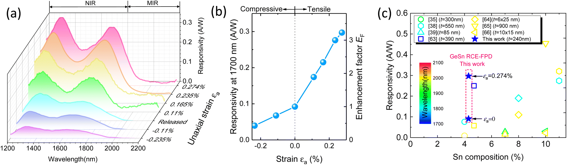
Thereafter, we investigated the optical responses of the GeSn RCE-FPDs under flat, bend-down, and bend-up conditions along 〈100〉 direction. The uniaxial strain induced by bending can be evaluated as62| |  | (3) |
where L ∼ 83 μm denotes the distance from the neutral plane of the device to the GeSn film of the GeSn RCE-FPD. Based on the analysis, we can determine the strain induced by mechanical bending, e.g., the tensile (compressive) strain was induced under bend-down (bend-up) conditions. The measured responsivity (Rλ) spectra of the GeSn RCE-FPD under flat and bending conditions are plotted in Fig. 5(a). Compared with the case of the flat condition, the optical responsivity significantly increased under the bend-down condition owing to the increasing tensile strain. In addition, the cutoff wavelength was slightly extended to a longer wavelength with increasing tensile strain. On the contrary, the optical responsivity significantly decreased under bend-up conditions, and the cutoff wavelength blue-shifted with the increasing compressive strain. In Fig. 5(b), the optical responsivity at λ = 1770 nm is portrayed as a function of the uniaxial strain, and the corresponding enhancement factor is defined as EF = Rλ(εa)/Rλ(εa = 0). With the application of the tensile strain, the responsivity increased significantly, and a notable enhancement factor up to 323% for εa = 0.274% was achieved, thereby validating sensitive photodetection. To demonstrate the competitiveness of our GeSn RCE-FPDs, Fig. 5(c) shows the comparison of the optical responsivity at room temperature for our GeSn RCE-FPD with selected reported GeSn PDs on rigid substrates35,38,39,63–66. It can be seen that, under flat condition (εa = 0), the optical responsivity of our GeSn RCE-FPDs is comparable with these GeSn PDs with Sn content of <5% and similar active layer thicknesses. With the application of εa = 0.274%, the optical responsivity is significantly enhanced, exhibiting superior optical responsivity compared to that of GeSn PDs. The optical responsivity is comparable to, or even better than, that of the GeSn PDs with higher Sn contents and/or thicker active layer, highlighting the competitiveness of our GeSn RCE-FPDs. Further enhancement of optical responsivity is possible by increasing the Sn content and/or the active layer thickness to enable more sensitive photodetection. With the flexibility, high responsivity, nontoxicity, and MIR detection capacity, the developed GeSn RCE-FPD establishes a new avenue for affordable high-performance MIR sensing with potential for flexible and wearable applications.
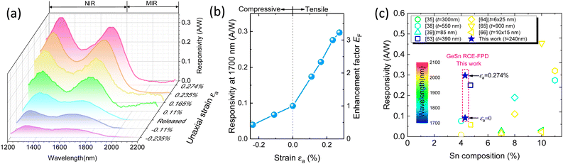 |
| | Fig. 5 (a) Room-temperature optical responsivity spectra of GeSn RCE-FPDs biased at 5 V under bending conditions. (b) Measured responsivity at λ = 1700 nm biased at 5 V as a function of uniaxial strain. (c) Comparison of optical responsivity of our GeSn RCE-FPDs with that of selected reported GeSn PDs on rigid substrates. | |
Conclusions
For the first time, this study demonstrated a new type of nontoxic strain-free GeSn MIR resonant-cavity-enhanced flexible photodetector fabricated using transfer-printing techniques. In principle, the GeSn nanomembrane was transferred to a PET flexible substrate to achieve flexibility and improve the material quality by eliminating the unwanted compressive strain and defective regions. A vertical cavity was created to enhance the responsivity, which was supported by our simulations. Under the bend-down conditions, the optical responsivity at 1970 nm was as high as 0.297 A W−1 with a tensile strain 0.274%, corresponding to an enhancement of 323% compared with the device without bending. These results demonstrate a new GeSn MIR flexible photodetector with high-performance and flexibility for a diverse range of applications.
Author contributions
Y. C. T. – Methodology, investigation, formal analysis, validation. A. S. – Methodology, investigation, formal analysis, validation. P. R. H. – Methodology, investigation. J. T. J. – Methodology, investigation. K. C. L. – Methodology, investigation. H. H. C. – Methodology, investigation, writing – review & editing. M. K. – Conceptualization, project administration, formal Analysis, writing – review & editing. G. E. C. – Conceptualization, supervision, project administration, formal analysis, writing – review & editing.
Conflicts of interest
There are no conflicts to declare.
Acknowledgements
This work at CCU was supported by the Young Scholar Fellowship Program by the Ministry of Science and Technology of Taiwan (MOST) under Grant no. MOST 111-2636-E-194-002 and MOST 110-2636-E-194-002. The work at Nanyang Technological University was supported by the A*STAR, Singapore, Advanced Manufacturing and Engineering (AME) Young Individual Research Grant (YIRG) under the Project A2084c0066, and Ministry of Education, Singapore, under the Grant ACRF Tier 2 grant (T2EP50120-0001) and Tier 1-2020-T1-002-020 (RG136/20). The authors also acknowledge the support of the Nanyang NanoFabrication Centre (N2FC).
References
-
R. Soref
, in Mid-Infrared Photonics, Optical Fiber Communication Conference (OFC), Optica 2015, paper W4A.4.
-
A. B. Seddon
, presented at 2014 16th Int. Conf. on Trans. Opt. Net. (ICTON), Graz, 6–10th July, 2014, pp. 1–4.
- A. B. Seddon, Phys. Status Solidi B, 2013, 250, 1020–1027 CrossRef CAS.
- T. Yokota, K. Fukuda and T. Someya, Adv. Mater., 2021, 33, 2004416 CrossRef CAS PubMed.
- D. Vilela, A. Romeo and S. Sánchez, Lab Chip, 2015, 16, 402–408 RSC.
- X. Guan, X. Yu, D. Periyanagounder, M. R. Benzigar, J.-K. Huang, C.-H. Lin, J. Kim, S. Singh, L. Hu, G. Liu, D. Li, J.-H. He, F. Yan, Q. J. Wang and T. Wu, Adv. Opt. Mater., 2021, 9, 2001708 CrossRef CAS.
- L. Du, C. Wang, W. Xiong, B. Wei, F. Yang, S. Chen, L. Ma, X. Wang, C. Xia, X. Zhang, Z. Wang and Q. Liu, Adv. Mater. Technol., 2020, 5, 1900853 CrossRef CAS.
- S. Cai, X. J. Xu, W. Yang, J. X. Chen and X. S. Fang, Adv. Mater., 2019, 31, 1808138 CrossRef PubMed.
- H. F. Ling, S. H. Liu, Z. J. Zheng and F. Yan, Small Methods, 2018, 2, 1800070 CrossRef.
- T. Jin, H.Y. G. Lin, T. Tiwald and P. T. Lin, Sci. Rep., 2019, 9, 4153 CrossRef PubMed.
- Y. Y. Zhang, Y. X. Zheng, J. Y. Lai, J. H. Seo, K. H. Lee, C. S. Tan, S. An, S. H. Shin, B. Son and M. Kim, ACS Nano, 2021, 15(5), 8386–8396 CrossRef CAS PubMed.
- X. Li, J. Zhang, C. Yue, X. Tang, Z. Gao, Y. Jiang, C. Du, Z. Deng, H. Jia, W. Wang and H. Chen, Sci. Rep., 2022, 12, 7681 CrossRef CAS PubMed.
- X. Jin, Y. Sun, Q. Wu, Z. Jia, S. Huang, J. Yao, H. Huang and J. Xu, ACS Appl. Mater. Interfaces, 2019, 11(45), 42385–42423 CrossRef CAS PubMed.
- N. Hong, D. Geum, T. S. Kim, S. Ahn, J. Han, D. Jung, G. Ryu, S. Kim, K. J. Yu and W. J. Choi, Adv. Photonics Res., 2021, 2, 2000051 CrossRef CAS.
- W. S. Ho, Y.-H. Dai, Y. Deng, C.-H. Lin, Y.-Y. Chen, C.-H. Lee and C. W. Liu, Appl. Phys. Lett., 2009, 94, 261107 CrossRef.
- M. Kim, J. H. Seo, Z. Yu, W. Zhou and Z. Ma, Appl. Phys. Lett., 2016, 109, 051105 CrossRef.
- S. Ghosh, K. C. Lin, C. H. Tsai, K. H. Lee, Q. Chen, B. Son, B. Mukhopadhyay, C. S. Tan and G. E. Chang, Opt. Express, 2020, 28, 23739–23747 CrossRef PubMed.
- J. Liu, D. D. Cannon, K. Wada, Y. Ishikawa, S. Jongthammanurak, D. T. Danielson, J. Michel and L. C. Kimerling, Appl. Phys. Lett., 2005, 87, 011110 CrossRef.
- G.-E. Chang, S.-W. Chen and H. H. Cheng, Opt. Express, 2016, 24, 17562–17571 CrossRef CAS PubMed.
- R. Kuroyanagi, L. M. Nguyen, T. Tsuchizawa, Y. Ishikawa, K. Yamada and K. Wada, Opt. Express, 2013, 21, 18553–18557 CrossRef CAS PubMed.
- R. Soref, Philos. Trans. R. Soc. London, Ser. A, 2014, 372, 20130113 CrossRef PubMed.
- G. E. Chang, S. W. Chang and S. L. Chuang, IEEE J. Quantum Electron., 2010, 46(12), 1813–1820 CAS.
- G. E. Chang, R. Basu, B. Mukhopadhyay and P. K. Basu, IEEE J. Sel. Top. Quantum Electron., 2016, 22(6), 8200409 Search PubMed.
- S. Ghosh, R. Bansal, G. Sun, R. A. Soref, H. H. Cheng and G. E. Chang, Sensors, 2022, 22, 3978 CrossRef CAS PubMed.
- G.-E. Chang, S.-Q. Yu, J. Liu, H. H. Cheng, R. A. Soref and G. Sun, IEEE J. Sel. Top. Quantum Electron., 2022, 28(2), 3800611 CAS.
- T. T. McCarthy, Z. Ju, S. Schaefer, S. Q. Yu and Y. H. Zhang, J. Appl. Phys., 2021, 130, 223102 CrossRef CAS.
- I. S. Yu, T. H. Wu, K. Y. Wu, H. H. Cheng, V. Mashanov, A. Nikiforov, O. Pchelyakov and X. S. Wu, AIP Adv., 2011, 1, 042118 CrossRef.
- M. Oehme, K. Kostecki, M. Schmid, F. Oliveira, E. Kasper and J. Schulze, Thin Solid Films, 2014, 557, 169–172 CrossRef CAS.
- Y. Miao, G. Wang, Z. Kong, B. Xu, X. Zhao, X. Luo, H. Lin, Y. Dong, B. Lu, L. Dong, J. Zhou, J. Liu and H. H. Radamson, Nanomaterials, 2021, 11(10), 2556 CrossRef CAS PubMed.
- M. A. Mircovich, C. Xu, D. A. Ringwala, C. D. Poweleit, J. Menéndez and J. Kouvetakis, ACS Appl. Electron. Mater., 2021, 3, 3451–3460 CrossRef CAS.
- J. Aubin, J. M. Hartmann, A. Gassenq, J. L. Rouviere, E. Robin, V. Delaye, D. Cooper, N. Mollard, V. Reboud and V. Calvo, Semicond. Sci. Technol., 2017, 32, 094006 CrossRef.
- J. Zheng, S. Wang, Z. Liu, H. Cong, C. Xue, C. Li, Y. Zuo, B. Cheng and Q. Wang, Appl. Phys. Lett., 2016, 108, 033503 CrossRef.
- J. Mathews, R. Roucka, J. Xie, S.-Q. Yu, J. Menéndez and J. Kouvetakis, Appl. Phys. Lett., 2009, 95, 133506 CrossRef.
- M. Oehme, M. Schmid, M. Kaschel, M. Gollhofer, D. Widmann, E. Kasper and J. Schulze, Appl. Phys. Lett., 2012, 101, 141110 CrossRef.
- H. H. Tseng, H. Li, V. Mashanov, Y. J. Yang, H. H. Cheng, G.-E. Chang, R. A. Soref and G. Sun, Appl. Phys. Lett., 2013, 103(23), 231907 CrossRef.
- S. Su, B. Cheng, C. Xue, W. Wang, Q. Cao, H. Xue, W. Hu, G. Zhang, Y. Zuo and Q. Wang, Opt. Express, 2011, 19(7), 6400 CrossRef CAS PubMed.
- S. Ghosh, K.-C. Lin, C.-H. Tsai, H. Kumar, Q. Chen, L. Zhang, B. Son, C. S. Tan, M. Kim, B. Mukhopadhyay and G.-E. Chang, Micromachines, 2020, 11, 795 CrossRef PubMed.
- H. Tran, T. Pham, W. Du, Y. Zhang, P. Grant, J. Grant, G. Sun, R. Soref, J. Margetis, J. Tolle, B. Li, M. Mortazavi and S. Q. Yu, J. Appl. Phys., 2018, 124(1), 013101 CrossRef.
- S. Xu, Y. C. Huang, K. H. Lee, W. Wang, Y. Dong, D. Lei, S. Panah, C. S. Tan, X. Gong and Y. C. Yeo, Opt. Express, 2018, 26(13), 17312–17321 CrossRef CAS PubMed.
- H. Tran, T. Pham, J. Margetis, Y. Zhou, W. Dou, P. C. Grant, J. M. Grant, S. Al-Kabi, G. Sun, R. A. Soref, J. Tolle, Y. H. Zhang, W. Du, B. Li, M. Mortazavi and S. Q. Yu, ACS Photonics, 2019, 6(11), 2807–2815 CrossRef CAS.
- W.-T. Hung, D. Barshilia, R. Basu, H. H. Cheng and G.-E. Chang, Opt. Lett., 2020, 45(5), 1088–1091 CrossRef CAS PubMed.
- Y.-H. Huang, G.-E. Chang, H. Li and H. H. Cheng, Opt. Lett., 2017, 42(9), 1652 CrossRef CAS PubMed.
- S. An, S. Wu, C. S. Tan, G. E. Chang, G. Xiao and M. Kim, J. Mater. Chem. C, 2020, 8, 13557–13562 RSC.
- C.-H. Tsai, K.-C. Lin, C.-Y. Cheng, K.-C. Lee, H. H. Cheng and G.-E. Chang, Opt. Lett., 2021, 46(4), 864–867 CrossRef PubMed.
- E. T. Simola, V. Kiyek, A. Ballabio, V. Schlykow, J. Frigerio, C. Zucchetti, A. De Iacovo, L. Colace, Y. Yamamoto, G. Capellini, D. Grützmacher, D. Buca and G. Isella, ACS Photonics, 2021, 8(7), 2166–2173 CrossRef.
- C. H. Liu, R. Bansal, C. Wu, Y. Jheng and G. Chang, GeSn, Adv. Photonics Res., 2022, 2100330 CrossRef CAS.
-
H. Tran, T. Pham, J. Margetis, Y. Zhou, W. Dou, P. C. Grant, J. M. Grant, S. Alkabi, W. Du, G. Sun, R. A. Soref, J. Tolle, B. Li, M. Mortazavi and S. Yu, Presented in Conference on Lasers and Electro-Optics (CLEO) (2019), paper STh4O.6.
- Y. C. Tai, P. L. Yeh, S. An, H. H. Cheng, M. Kim and G. E. Chang, Nanotechnology, 2020, 31(44), 445301 CrossRef CAS PubMed.
- M. R. Atalla, S. Assali, A. Attiaoui, C. L. Leduc, A. Kumar and S. Abdi, Adv. Funct. Mater., 2021, 31, 2006329 CrossRef CAS.
- Q. Chen, S. Wu, L. Zhang, H. Zhou, W. Fan and C. S. Tan, Nanoscale, 2022, 14, 7341–7349 RSC.
-
S. L. Chuang, Physics of Photonic Devices, Wiley, New York, 2nd edn, 2009 Search PubMed.
- Z. Cheng, T. Zhao and H. Zeng, Small Sci., 2022, 2, 2100051 CrossRef CAS.
- L.-H. Zeng, D. Wu, S.-H. Lin, C. Xie, H.-Y. Yuan, W. Lu, S. P. Lau, Y. Chai, L.-B. Luo, Z.-J. Li and Y. H. Tsang, Adv. Funct. Mater., 2019, 29, 1806878 CrossRef.
- A. K. Okyay, C. O. Chui and K. Saraswat, Appl. Phys. Lett., 2006, 88, 063506 CrossRef.
- S. Averine, O. Bondarenko and R. Sachot, Solid-State Electron., 2002, 46, 2045–2051 CrossRef CAS.
- X. Li, L. Peng, Z. Liu, Z. Zhou, J. Zheng, C. Xue, Y. Zuo, B. Chen and B. Cheng, Photonics Res., 2021, 9, 494–500 CrossRef.
- S. Ghosh, H. Kumar, B. Mukhopadhyay and G. E. Chang, IEEE Sens. J., 2021, 12(8), 9900–9908 Search PubMed.
- S. Ghosh, R. Bansal, G. Sun, R. A. Soref, H. H. Cheng and G. E. Chang, Sensors, 2022, 22, 3978 CrossRef CAS PubMed.
- S. An, Y. C. Tai, K. C. Lee, H. H. Cheng, G. E. Chang and M. Kim, Nanotechnology, 2021, 32, 355704 CrossRef CAS PubMed.
-
E. D. Palik, Handbook of Optical Constants of Solids, Academic, Orlando, Florida, USA, 1985 Search PubMed.
- H. Tran, W. Du, S. A. Ghetmiri, A. Mosleh, G. Sun, R. A. Soref, J. Margetis, J. Tolle, B. Li, H. A. Naseem and S. Q. Yu, J. Appl. Phys., 2016, 119(10), 103106 CrossRef.
-
R. C. Hibbeler, Mechanics of Materials, Prentice Hall, Boston, USA, 10th edn, 2017 Search PubMed.
- C. H. Tsai, B. J. Huang, R. A. Soref, G. Sun, H. H. Cheng and G. E. Chang, Opt. Lett., 2020, 45, 1463 CrossRef PubMed.
- H. Zhou, S. Xu, Y. Lin, Y. Huang, B. Son, Q. Chen, X. Guo, K. H. Lee, S. C. Goh, X. Gong and C. S. Tan, Opt. Express, 2020, 28, 10280 CrossRef PubMed.
- Q. Chen, S. Wu, L. Zhang, D. Burt, H. Zhou, D. Nam, W. Fan and C. S. Tan, Opt. Lett., 2021, 46, 3809 CrossRef CAS PubMed.
- Y. Dong, W. Wang, S. Xu, D. Lei, X. Gong, X. Guo, H. Wang, S. Y. Lee, W. K. Loke, S. F. Yoon and Y. C. Yeo, Opt. Express, 2017, 25, 15818 CrossRef CAS PubMed.
|
| This journal is © The Royal Society of Chemistry 2023 |
Click here to see how this site uses Cookies. View our privacy policy here. 
 Open Access Article
 This Open Access Article is licensed under a Creative Commons Attribution-Non Commercial 3.0 Unported Licence
 *b and
Guo-En
Chang
*b and
Guo-En
Chang