Atomic layer deposition of SnO2 using hydrogen peroxide improves the efficiency and stability of perovskite solar cells

Sang-Uk Lee a, Hyoungmin Park b, Hyunjung Shin bc and Nam-Gyu Park *ac
aSchool of Chemical Engineering, Center for Antibonding Regulated Crystals, Sungkyunkwan University, Suwon 16419, Republic of Korea. E-mail: npark@skku.edu
bDepartment of Energy Science, Sungkyunkwan University, Suwon 16419, Republic of Korea
cSKKU Institute of Energy Science and Technology (SIEST), Sungkyunkwan University, Suwon 16419, Republic of Korea

Received 9th December 2022 , Accepted 3rd February 2023

First published on 6th February 2023


Abstract

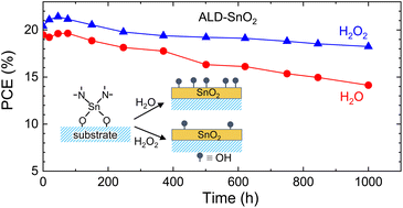
Low-temperature processed SnO2 is a promising electron transporting layer in perovskite solar cells (PSCs) due to its optoelectronic advantage. Atomic layer deposition (ALD) is suitable for forming a conformal SnO2 layer on a high-haze substrate. However, oxygen vacancy formed by the conventional ALD process using H2O might have a detrimental effect on the efficiency and stability of PSCs. Here, we report on the photovoltaic performance and stability of PSCs based on the ALD-SnO2 layer with low oxygen vacancies fabricated via H2O2. Compared to the ALD-SnO2 layer formed using H2O vapors, the ALD-SnO2 layer prepared via H2O2 shows better electron extraction due to a reduced oxygen vacancy associated with the highly oxidizing nature of H2O2. As a result, the power conversion efficiency (PCE) is enhanced from 21.42% for H2O to 22.34% for H2O2 mainly due to an enhanced open-circuit voltage. Operational stability is simultaneously improved, where 89.3% of the initial PCE is maintained after 1000 h under an ambient condition for the H2O2-derived ALD SnO2 as compared to the control device maintaining 72.5% of the initial PCE.


Introduction

Since the report on all-solid-state PSCs with a PCE of 9.7% and nondegraded stability for 500 h in 2012,1 PSCs have received tremendous attention due to low cost and high efficiency. As a result, a certified PCE of 25.7% has been achieved in 2022.2 Such superb photovoltaic performance was realized by excellent intrinsic optoelectronic properties of the perovskite material with high absorption coefficient, diffusion length, defect-tolerance properties,3–6 and compositional engineering and manufacturing processes such as interfacial, additive, and precursor engineering.7–11 Besides the perovskite layer, charge transport materials and junction between perovskite and charge transport layers are critical in determining photovoltaic performance. Thus, the selection of suitable materials and methods to fabricate charge transport layers are important to achieving high efficiency and stability of PSCs. For the n-i-p device structure, the electron transport layer (ETL) plays a crucial role, not only in electron extraction but also in providing a substrate for perovskite film growth. Among the studied ETLs, the wide bandgap SnO2 formed at low temperatures is widely used for ETL because of high carrier mobility, low-temperature processibility, and photo-inactive nature under UV illumination.12–15 Various coating methods have been reported to fabricate SnO2 thin films including chemical bath deposition,16 spray-pyrolysis,17 and atomic layer deposition (ALD).18–21 ALD is one of the beneficial techniques for conformal and uniform coating compared to other methods.22–24 When using H2O and the tetrakis(dimethylamino) tin (TDMASn) precursor to deposit SnO2 thin films in ALD, compared with hydrogen peroxide (H2O2) and ozone (O3), an oxygen vacancy is often generated due to slow kinetics associated with uneasy removal of ligands in the precursor from the SnO2 surface.25,26 As a result, these oxygen vacancies can cause poor performance and instability because they act as a recombination site for carriers.27,28 Thus, it is interesting to compare the photovoltaic performance of PSCs between the H2O-derived ALD SnO2 and the H2O2-derived one.

Here, we report on the highly oxidizing H2O2 as an oxygen vapor source for preparing the SnO2 thin film in ALD. Photovoltaic performance and stability for the H2O2-derived SnO2 films are compared with those for the H2O-derived ones. Better extraction of the photoexcited electrons from perovskite to SnO2 is observed for the H2O2-derived SnO2 than for the H2O-derived one due to reduced surface oxygen defects. As a result, higher photovoltaic performance and improved stability are achieved using H2O2 during ALD. This work provides important insight into the carrier material design for oxide films in ALD.

Results and discussion

The ALD process is schematically illustrated in Fig. 1, where one cycle of ALD comprising two half cycles in between purging cycles is repeated to form oxide thin films. In the first half cycle shown in Fig. 1(a), the gaseous TDMASn precursor is pulsed to react with the hydroxyl-functionalized surface on the substrate, followed by purging Ar to remove the byproduct of dimethylamine and unreacted precursor. For the second half cycle in Fig. 1(b), an oxygen source, such as H2O or H2O2 is pulsed to react with the surface adsorbed DMA-Sn-O, followed by purging Ar to eliminate byproducts of dimethylamine and O2. Since oxygen defect may be formed due to the surface hydroxyl group, leading to SnO2−x(OH)x, an oxygen source with higher oxidizing and better proton transfer capability, such as H2O2, is expected to be better in defect-less SnO2.29–31
image file: d2nr06884b-f1.tif
Fig. 1 The schematic illustration of (a) the first half cycle and (b) the second half cycle of the ALD process to form SnO2 using TDMASn and H2O2, together with chemical reactions. A hydroxyl-functionalized substrate was assumed.

X-ray photoelectron spectroscopy (XPS) was carried out to investigate the oxidation state of tin and oxygen vacancy of the ALD-deposited SnO2 film. As shown in Fig. 2(a), the binding energies of Sn 3d5/2 (487.18 eV) and Sn 3d3/2 (495.58 eV) for the H2O2-derived SnO2 are slightly higher than the corresponding 486.88 eV and 495.33 eV for the H2O-derived one. The spin–orbit splitting of about 8.4 eV and binding energies indicate that the oxidation state of tin is close to being tetravalent.32 The slightly higher binding energies observed for the H2O2-derived SnO2 implies that the oxidation state of tin in the H2O2-derived SnO2 is relatively higher than that in the H2O-derived one,33–36 which might be due to the stronger oxidizing characteristics of H2O2. Oxygen 1s XPS spectra in Fig. 2(b) for H2O and Fig. 2(c) for H2O2 are deconvoluted into two peaks that correspond to the oxygen on the surface of SnO2 (OSn) and chemisorbed oxygen or hydroxyl-related oxygen (OOH).37–40 The binding energies for each species and fraction of OOH are listed in Table S1. The fraction of OOH decreased from 25.47% to 21.36% upon replacing H2O with H2O2, indicative of the suppression of oxygen vacancy (defect) by H2O2 during the preparation of SnO2.


image file: d2nr06884b-f2.tif
Fig. 2 (a) Sn 3d and (b and c) O 1s XPS spectra of the ALD-SnO2 films based on H2O and H2O2 oxygen source. The binding energy was calibrated using the C 1s binding energy of 284.78 eV. The raw data (black empty circles) in O 1s data were deconvoluted to two peaks (blue lines: hydroxyl oxygen (OOH), green lines: oxygen in Sn–O (OSn), and purple lines: baseline).

To understand the dependence of perovskite morphology on the SnO2 film formed from different oxygen sources in the ALD process, scanning electron microscopy (SEM) images of the perovskite films were collected. According to the cross-sectional SEM images shown in Fig. 3(a) and (c), the mean thickness of the perovskite film was slightly thicker for the H2O2-derived SnO2 (549.4 ± 69.2 nm) than the H2O-derived one (518.8 ± 29.3 nm) and the entire film morphology including the surface flatness is better for the perovskite film grown on the H2O2-derived SnO2. This indicates that the H2O2-derived SnO2 layer is beneficial for the growth of high-quality perovskite film. Furthermore, the perovskite grain size was also increased from 893.0 nm for H2O to 1046.9 nm for H2O2 (Fig. 3(b) and (d)), which is beneficial for the reduction of grain boundaries. A contour-line-like surface morphology observed from the H2O2-derived SnO2 is indicative of improvement of the perovskite crystallinity.41


image file: d2nr06884b-f3.tif
Fig. 3 (a and c) Cross-sectional and (b and d) top-view SEM images of the perovskite films formed on (a and b) the H2O-derived SnO2 and (c and d) the H2O2-derived SnO2. Insets are size distributions.

To understand the change in the surface morphology of ALD-SnO2 depending on H2O and H2O2, top-view SEM and atomic force microscopy (AFM) images were captured, as shown in Fig. S1. Although the difference in surface morphology of the ALD-SnO2 is hard to figure out from the top-view SEM images, the surface roughness in the AFM image was reduced from 36.43 nm for H2O to 32.02 nm for H2O2. The reduced surface roughness of the SnO2 film would be beneficial for better contact with the perovskite,42 which is one of the factors responsible for the improved Voc and FF. To investigate the effect of the oxygen source on the optical properties of the perovskite film and the photon-to-electron conversion efficiency of PSCs in the ALD process, UV-Vis spectroscopy and external quantum efficiency (EQE) were performed and the data are shown in Fig. S2. The absorbance of the perovskite films hardly changed regardless of the oxygen source. In addition, an optical band gap calculated from the Tauc plot was about 1.55 eV, which is also unaffected by the oxygen source. The EQE spectral shape for H2O2 is almost identical to that for H2O, except for the slightly higher integrated Jsc of 23.87 mA cm−2 for H2O2 than 23.61 mA cm−2 for H2O.

The effect of the oxygen source on charge separation and carrier lifetime was studied using steady-state photoluminescence (SSPL) and time-resolved photoluminescence (TRPL). As seen in Fig. 4(a), the PL emission intensity of the bare perovskite film was significantly decreased in the presence of the SnO2 layer due to electron injection from perovskite to SnO2. PL quenching is more pronounced for the H2O2-derived SnO2 than for the H2O-derived one, which is probably due to the reduced oxygen defects, as observed in the O 1s XPS study (see Fig. 2). The TRPL decay curves in Fig. 4(b) were fitted with a biexponential decay equation of I(t) = I0 + A1exp(−(tt0)/τ1) + A2exp(−(tt0)/τ2), where I(t) is the time-dependent PL intensity, τ1 is the fast decay component attributed to the quenching of charge carriers in the interface, and τ2 is the slow decay component related to the radiative recombination of free charge carriers in the bulk.43–45 The detailed parameters are summarized in Table S2. The perovskite film deposited on the glass substrate showed the longest lifetime of τ1 = 104.5 ns and τ2 = 1957.3 ns because there is no layer to transfer the charges from the perovskite layer, which is consistent with the values reported elsewhere.46 For the perovskite film deposited on the H2O2-derived SnO2, τ1 and τ2 were reduced to 46.7 ns and 390.3 ns, respectively, while 71.3 ns and 486.7 ns were observed for the H2O-derived one. The reduced time constants ascribed to the charge transfer from perovskite to SnO2 and the faster decay in PL for the H2O2-derived SnO2 are indicative of the faster charge separation, probably due to the improved interface.47


image file: d2nr06884b-f4.tif
Fig. 4 (a) Steady-state PL and (b) TRPL of perovskite films deposited on glass with and without ALD-SnO2 layer. Lines represent the fitted results in TRPL. (c) Dark IV characteristics of the FTO/SnO2/Au devices. (d) TPV and (e) TPC data. Data were fit with the biexponential decay equation, which is represented as lines. (f) Nyquist plots obtained in the frequency range of 1 MHz to 0.1 Hz under one sun illumination at a bias of 1.0 V with the device structure of the FTO/SnO2/perovskite/Spiro-MeOTAD/Au. Inset is the equivalent circuit, where Rs, Rct, Rrec, CPE1, and CPE2 represent series resistance, resistance for charge transport, resistance for charge recombination, constant phase element 1, and constant phase element 2, respectively.

Dark current–voltage (IV) characteristics of the electron-only device (FTO/ETL/Au) were investigated to analyze the conductivity of the ALD-SnO2 (Fig. 4(c)). Conductivity can be estimated from σ = Id/VA, where σ, d, and A are the conductivity, the thickness of the ETL film, and the area of the sample, respectively.48,49 Although SnO2 is a wide-bandgap oxide that is essentially an insulator, the electrical conductivity of the H2O2-derived SnO2 film was estimated to be 4.43 × 10⁻⁴ mS cm−1, which is slightly higher than 3.11 × 10⁻⁴ mS cm−1 of the H2O-derived SnO2. The improvement of charge extraction transport at the H2O2-derived SnO2 is thus related to the relatively improved conductivity due to surface passivation, which seems to contribute to the improvement of FF.48,50 To examine the charge recombination and electron transport ability of ETL in the full device structure (FTO/SnO2/perovskite/spiro-MeOTAD/Au), transient photovoltage (TPV) and transient photocurrent (TPC) decay were measured (Fig. 4(d) and (e)) and fitted by using a biexponential decay equation.51,52 TPV decay was measured at open-circuit conditions, where the increase of photovoltage lifetime is indicative of the longer recombination lifetime of holes and electrons. The TPV decay time for the H2O2-derived SnO2 was estimated to be 0.530 ms, which is longer than 0.389 ms for the H2O-derived SnO2, suggesting that the SnO2 layer formed by H2O2 vapor is more beneficial for the reduction of the nonradiative recombination.53,54 TPC decay measured under short-circuit condition, where the decrease in photocurrent decay time implies that charge carrier transport becomes faster. The photocurrent decay was shortened from 0.151 μs for the H2O case to 0.076 μs upon using H2O2. According to the data from TPV and TPC, higher Voc for the H2O2-derived SnO2 is attributed to the reduction of recombination.

To further analyze the increase of Voc and FF for the H2O2-derived SnO2, electrochemical impedance spectroscopy (EIS) study was carried out to examine the interfacial charge transfer and recombination. In Fig. 4(f), Nyquist plots of the full devices (FTO/SnO2/perovskite/Spiro-MeOTAD/Au) are shown in the frequency range of 1 MHz to 0.1 Hz under one sun illumination at a bias of 1.0 V. Two semicircles were observed, where the first semicircle in the high-frequency region is related to the charge transport resistance (Rct) at the interface and the second semicircle in the low-frequency region correlates with the charge recombination resistance (Rrec).55–57Rct for the H2O2-derived SnO2 is 111.2 Ω, which is lower than 127.9 Ω for the H2O-derived one. On the other hand, Rrec was increased from 38.3 Ω for the H2O-derived SnO2 to 48.4 Ω for the H2O2-derived SnO2. The values obtained for Rct and Rrec under one sun illumination at a bias of 1.0 V close to the Voc are consistent with those reported elsewhere.55,56 In addition, the fact that Rrec is lower than Rct might be due to the dielectric relaxation by an interfacial ion reorganization and charge accumulation of perovskite in the low-frequency region under one sun illumination.56–58 Thus, the lower Rct and higher Rrec for the H2O2-derived SnO2 than for the H2O-derived one is responsible for higher FF and Voc due to the improved charge transport and reduced recombination.37,59

The energy band alignment of ETL and the perovskite layer were studied using ultraviolet photoelectron spectroscopy (UPS), Fig. S3, and UV-Vis spectroscopy, Fig. S4. The work function was measured by the difference between He I radiation (21.22 eV) and Ecut-off (cut-off energy in the high binding energy region). The valence band maximum (VBM) can be determined by the sum of the Fermi level acquired with the work function and the energy obtained in the low binding energy region of the logarithmic-scale curve (Fig. S3). Finally, the conduction band maximum (CBM) can be determined using an optical bandgap estimated by the Tauc plot (Fig. S4 (a)). The energy band diagram is represented in Fig. S4(b). The band gap of the SnO2 layer (3.96 eV) is unchanged; however, the CBM of the H2O2-derived SnO2 is upshifted from −4.65 eV to −4.53 eV as compared to the H2O-derived one, which is closer to CBM of −4.32 eV for perovskite. The Fermi level is also upshifted from −5.15 eV to −5.03 eV by changing the oxygen source from H2O to H2O2, which is also closer to that of −4.89 eV for perovskite. Thus, the band alignment between perovskite and the H2O2-derived SnO2 is beneficial for better Voc and FF.60

The current density–voltage (JV) curves and photovoltaic parameters for the H2O- and H2O2-derived SnO2 films are shown in Fig. S5 and Table S3. The reverse scanned PCE for the H2O-derived SnO2 is 17.71% with short-circuit photocurrent density (Jsc) of 24.20 mA cm−2, open-circuit voltage (Voc) of 1.0685 V, and fill factor (FF) of 0.69. The device with the H2O2-derived SnO2 improves PCE to 19.09% mainly due to the enhanced Voc of 1.0973 V and FF of 0.72 with a similar Jsc of 24.30 mA cm−2. The improvement of Voc and FF might be attributed to the improved interface between the H2O2-derived SnO2 and perovskite.

Since the PCE was not as high as the reported value of over 20%, the ALD-SnO2 layer was over-deposited with colloidal SnO2via the spin-coating process. Fig. 5(a) shows the JV curves of the best-performing PSCs based on the bilayered SnO2 comparing the H2O- or H2O2-derived ALD SnO2 film that was overcoated with the colloidal SnO2via spin-coating. The photovoltaic parameters are listed in Table S4. The bilayer SnO2 films exhibit higher PCEs than the only ALD-SnO2 case. The reverse scanned PCE of 21.42% was achieved from the bilayer SnO2 based on the H2O-derived SnO2 due to Jsc of 24.07 mA cm−2, Voc of 1.1175 V, and FF of 0.80, whereas higher PCE of 22.34% was obtained from the bilayer based on the H2O2-derived SnO2 mainly due to the increased Voc of 1.1460 V. The statistical photovoltaic parameters shown in Fig. 5(b–e) and Table S5 indicate that the average PCE of 21.73 ± 0.44% for the H2O2 approach is higher than the 20.64 ± 0.38% observed for the H2O method.


image file: d2nr06884b-f5.tif
Fig. 5 (a) JV curves of the best performing PSC with a bilayer of ALD-SnO2/spin-coated SnO2. Dashed and solid lines represent forward and reverse scanned data, respectively. (b) Statistical photovoltaic parameters of Jsc, Voc, FF, and PCE for a bilayer SnO2 with the H2O-derived SnO2 and the H2O2-derived one. Diagonal lines and empty squares represent forward-scanned and reverse-scanned data, respectively.

Steady-state PCE was examined for 1200 s at the maximum power point under one sun illumination without encapsulation. Fig. 6(a) shows that PSC based on the H2O2-derived ALD-SnO2/colloidal SnO2 bilayer maintains 97.90% of the initial PCE, whereas PCE declined down to 95.84% for the H2O-derived ALD-SnO2/colloidal SnO2 bilayer. Finally, storage stability was investigated for 1000 h at ambient conditions of a temperature of 25 ± 5 °C and relative humidity of 30 ± 5%. Fig. 6(b) shows that 89.3% of the initial PCE was maintained for the H2O2-derived SnO2 system after 1000 h, while 72.5% of the initial PCE was retained for PSC based on the H2O-derived SnO2. Normalized photovoltaic parameters are presented in Fig. S6, where the degraded performance in the H2O-derived SnO2 system is mainly due to the relatively pronounced degradation of FF. A relatively poor interface between the perovskite and the H2O-derived SnO2 might accelerate the degradation of FF. It has been reported that the charges trapped between the ETL and perovskite layer by the interfacial defects could initiate degradation of the performance and stability of PSCs under the moisture condition.61 Thus, it is important to manage the ETL surface for improving the stability and efficiency of PSCs and our work can give important insight into the control of the SnO2 surface via the oxygen source in ALD.


image file: d2nr06884b-f6.tif
Fig. 6 Comparison of the stability of the H2O2-derived SnO2-based PSC with the H2O-derived SnO2-based PSC using (a) steady-state PCE measured at maximum power points (0.922 V for H2O and 0.935 V for H2O2) for 1200 s and (b) storage stability for 1000 hours under a relative humidity of about 30% at room temperature.

Conclusions

The photovoltaic performance and stability of PSCs based on ALD-SnO2 were studied depending on the oxygen source of H2O and H2O2. The surface oxygen defect of ALD-SnO2 was reduced by changing H2O with H2O2. As a result, the ALD-SnO2/perovskite interface was improved by using H2O2 and thereby, the separation of the excited electrons was better for the H2O2-derived SnO2 than for the H2O-derived SnO2. Since the ALD-SnO2 plays a substrate role, the perovskite film grown at the H2O2-derived SnO2 layer was better in quality than that grown at the H2O-derived one. PCE of 22.34% was achieved using the H2O2-derived ALD-SnO2, which was better than that obtained using the conventional oxygen source of H2O in ALD. Furthermore, the improved SnO2/perovskite interface using H2O2 led to the enhancement of device stability. From the current study, the control of SnO2 defects is found to be critical in achieving better efficiency and stability of PSCs.

Experimental

Synthesis of materials

Formamidnium iodide, HC(NH2)2I (FAI), was synthesized by reacting 30 mL hydroiodic acid (57 wt% in water, Sigma Aldrich) with 20 g of formamidnium acetate (99%, Sigma Aldrich) in an ice bath for 1 h. The brown precipitate was collected by an evaporating solvent at 60 °C for 30 min using a rotary evaporator. The collected powder was washed with diethyl ether (>99.0%, Sigma Aldrich) to obtain a white precipitate. The product was recrystallized in ethyl alcohol (99.9%, Sigma Aldrich). The recrystallization process was repeated three times to achieve pure FAI powder that was finally washed with diethyl ether. The FAI powder was collected by filtration and dried for 24 h under a vacuum. Methylammonium bromide, CH3NH3Br (MABr), was synthesized in a similar method by using hydrogen bromide (HBr, 48 wt% in H2O, Sigma-Aldrich) and methylamine (CH3NH2, 40% in methanol, TCI).

The FAPbI3 single crystals were synthesized by inverse temperature crystallization using a 1.6 M γ-butyrolactone (GBL, 99.5%, SamChun Chemicals) solution of equimolar FAI and PbI2 (99%, Acros) at 80 °C for 30 min and at 130 °C for 3 h. The product was washed with acetonitrile and diethyl ether, followed by drying at 150 °C for 30 min. The MAPbBr3 single crystals were synthesized in a similar method by using PbBr2 (>98%, Sigma Aldrich) and the synthesized MABr in N,N′-dimethylformamide (DMF, 99.8% anhydrous, Sigma Aldrich).

Device fabrication

Fluorine-doped tin oxide (FTO) conductive glass substrates (2.4 cm × 2.4 cm, Pilkington, TEC-8, 8 Ω sq−1) were ultrasonically cleaned with detergent, deionized (DI) water, acetone, and ethanol in sequence for 10 min. The cleaned FTO substrates were treated with ultraviolet ozone (UVO) for 40 min before the deposition of the SnO2 layer by ALD. For the deposition of SnO2 by a hand-made ALD system, H2O or H2O2 (35 wt% in H2O, Sigma Aldrich) as an oxygen source and tetrakis(dimethylamino) tin(IV) (TDMASn) (EGCHEM Co., Ltd (Daejeon, Korea)) as a tin precursor were used. The TDMASn precursor was maintained at 50 °C and the deposition was carried out at 100 °C with 84 cycles to obtain 10 nm thickness. One cycle was composed of TDMASn pulse for 0.3 s, Ar purging for 12 s, oxygen source pulse for 0.05 s, and Ar purging for 17 s,21 under 5 × 10⁻² torr with Ar flow of 30 sccm were performed. For the improvement of the photovoltaic performance of PSCs, the ALD-SnO2 layer was further overcoated with colloidal SnO2 by spin coating a 2 wt% aqueous colloidal SnO2 solution (15 wt% stock solution (Alfa Aesar) was diluted) at 4000 rpm for 20 s, which was sintered at 190 °C for 30 min on a hot plate.

The (FAPbI3)0.96(MAPbBr3)0.04 perovskite precursor solution was prepared by mixing 972.3 mg and 30.7 mg of the synthesized FAPbI3 and MAPbBr3 single crystals, respectively, in 111 μL of dimethyl sulfoxide (DMSO, >99.5%, Sigma Aldrich) and 889 μL of DMF, where 32.4 mg MACl was added as an additive. The perovskite solution was spin-coated on the SnO2 layer at 1000 rpm for 5 s and 5000 rpm for 20 s, where 1 mL of diethyl ether was dripped on the rotating substrate at 10 s before the end of spin coating, followed by annealing at 150 °C for 15 min and 100 °C for 15 min on a hot plate. The 2,2′,7,7′-tetrakis-(N,N-di-4-methoxyphenylamino)-9,9′-spirobifluorene (spiro-MeOTAD) stock solution was prepared by mixing 90 mg of spiro-MeOTAD (99%, Sigma Aldrich), 39.5 μL of 4-tert-butyl pyridine (4-tBP, 98%, Sigma Aldrich), 23 μL of lithium bis(trifluoromethanesulfonyl)imide (Li-TFSI) stock solution (520 mg Li-TSFI (Sigma Aldrich) in 1 mL ACN (99.8%, Sigma Aldrich)) and 10 μL of tris(2-(1H-pyrazol-1-yl)-4-tert-butylpyridine) cobalt(III) tri[bis(trifluoromethane)sulfonimide] (Co-TFSI) stock solution (375 mg Co-TSFI (Sigma Aldrich) in 1 mL ACN) in 1 mL of chlorobenzene (99.8%, Sigma Aldrich). 25 μL of spiro-MeOTAD solution was spin-coated on the perovskite film at 3000 rpm for 30 s. Finally, a ∼70 nm-thick Au electrode was deposited by a thermal evaporator.

Characterization

Current density–voltage (JV) characteristics were obtained using a Keithely 2400 source meter under AM 1.5G one sun (100 mW cm−2) illumination using a solar simulator (Oriel Sol 3A, class AAA) equipped with 450 W Xenon lamp (Newport 6280NS). The light intensity was adjusted by an NREL-calibrated Si solar cell having a KG-5 filter. The aperture area was 0.125 cm2. X-ray photoelectron spectroscopy (XPS) was measured using the ESCALAB 250 XPS system (Thermo Fisher Scientific) with Al Kα X-ray radiation (1486.6 eV). Ultraviolet photoelectron spectroscopy (UPS) was performed with the ESCALAB 250 XPS system (Thermo Fisher Scientific) using He I (21.2 eV). External quantum efficiency (EQE) spectra were obtained using a QEX-7 series system (PV measurements Inc.) by a monochromatic beam generated from a 75 W xenon source lamp (USHIO, Japan) in DC mode. Absorption spectra were obtained using a UV-vis spectrometer (Lambda 45, PerkinElmer). PL was measured using a Quantarus Tau compact fluorescence lifetime spectrometer (Quantarus Tau C11367 12, Hamamatsu) with a 464 nm laser pulsed at a repetition frequency of 10 MHz for steady-state PL and 5 MHz for TRPL. Electrochemical impedance spectroscopy data were collected using an Autolab 302B from a frequency range of 10−1 to 106 Hz and fitted using the Z-view software.

Author contributions

N.-G. P. and S.-U. L. conceived the idea and wrote the manuscript. S-U. L. carried out the fabrication of devices, measurements, and analysis of the data. H. P. and S.-U. L. constructed a homemade ALD. H. S. provided the methodology for ALD deposition and edited the manuscript.

Conflicts of interest

There are no conflicts to declare.

Acknowledgements

This work was supported by the National Research Foundation of Korea (NRF) grants funded by the Ministry of Science and ICT (MSIT) of Korea under contracts NRF-2021R1A3B1076723 (Research Leader Program) and NRF-2022M3J1A1063226 and NRF-2022M3J1A1085280 (Carbon Neutral Technology Program). H. S. also acknowledges financial support with NRF-2019R1A2C3009157. This work was in part supported by the Korea Evaluation Institute of Industrial Technology under contract 20016588.

References

  1. H.-S. Kim, C.-R. Lee, J.-H. Im, K.-B. Lee, T. Moehl, A. Marchioro, S.-J. Moon, R. Humphry-Baker, J.-H. Yum, J. E. Moser, M. Grätzel and N.-G. Park, Sci. Rep., 2012, 2, 591 CrossRef PubMed.
  2. M. Kim, J. Jeong, H. Lu, T. K. Lee, F. T. Eickemeyer, Y. Liu, I. W. Choi, S. J. Choi, Y. Jo, H.-B. Kim, S.-I. Mo, Y.-K. Kim, H. Lee, N. G. An, S. Cho, W. R. Tress, S. M. Zakeeruddin, A. Hagfeldt, J. Y. Kim, M. Grätzel and D. S. Kim, Science, 2022, 375, 302–306 CrossRef CAS PubMed.
  3. J. Y. Kim, J.-W. Lee, H. S. Jung, H. Shin and N.-G. Park, Chem. Rev., 2020, 120, 7867–7918 CrossRef CAS PubMed.
  4. Q. Dong, Y. Fang, Y. Shao, P. Mulligan, J. Qiu, L. Cao and J. Huang, Science, 2015, 347, 967–970 CrossRef CAS PubMed.
  5. S. D. Stranks, G. E. Eperon, G. Grancini, C. Menelaou, M. J. P. Alcocer, T. Leijtens, L. M. Herz, A. Petrozza and H. J. Snaith, Science, 2013, 342, 341–344 CrossRef CAS PubMed.
  6. B. Li, B. Chang, L. Pan, Z. Li, L. Fu, Z. He and L. Yin, ACS Energy Lett., 2020, 5, 3752–3772 CrossRef CAS.
  7. J. Chen and N.-G. Park, ACS Energy Lett., 2020, 5, 2742–2786 CrossRef CAS.
  8. W. A. Dunlap-Shohl, Y. Zhou, N. P. Padture and D. B. Mitzi, Chem. Rev., 2019, 119, 3193–3295 CrossRef CAS PubMed.
  9. F. Zhang and K. Zhu, Adv. Energy Mater., 2020, 10, 1902579 CrossRef CAS.
  10. J. Chen and N.-G. Park, Adv. Mater., 2019, 31, 1803019 CrossRef CAS PubMed.
  11. T. Li, Y. Pan, Z. Wang, Y. Xia, Y. Chen and W. Huang, J. Mater. Chem. A, 2017, 5, 12602–12652 RSC.
  12. G. Yang, C. Chen, F. Yao, Z. Chen, Q. Zhang, X. Zheng, J. Ma, H. Lei, P. Qin, L. Xiong, W. Ke, G. Li, Y. Yan and G. Fang, Adv. Mater., 2018, 30, 1706023 CrossRef PubMed.
  13. L. Qiu, Z. Liu, L. K. Ono, Y. Jiang, D.-Y. Son, Z. Hawash, S. He and Y. Qi, Adv. Funct. Mater., 2019, 29, 1806779 CrossRef CAS.
  14. W. Ke, G. Fang, Q. Liu, L. Xiong, P. Qin, H. Tao, J. Wang, H. Lei, B. Li, J. Wan, G. Yang and Y. Yan, J. Am. Chem. Soc., 2015, 137, 6730–6733 CrossRef CAS PubMed.
  15. P. Tiwana, P. Docampo, M. B. Johnston, H. J. Snaith and L. M. Herz, ACS Nano, 2011, 5, 5158–5166 CrossRef CAS PubMed.
  16. D. Wang, T. He, S. Li, Y. Jiang and M. Yuan, ACS Appl. Energy Mater., 2022, 5, 5340–5347 CrossRef CAS.
  17. W. Long, A. He, S. Xie, X. Yang and L. Wu, Energies, 2022, 15, 3211 CrossRef CAS.
  18. C. Wang, L. Guan, D. Zhao, Y. Yu, C. R. Grice, Z. Song, R. A. Awni, J. Chen, J. Wang, X. Zhao and Y. Yan, ACS Energy Lett., 2017, 2, 2118–2124 CrossRef CAS.
  19. L. Kavan, L. Steier and M. Grätzel, J. Phys. Chem. C, 2017, 121, 342–350 CrossRef CAS.
  20. S. Jeong, S. Seo, H. Park and H. Shin, Chem. Commun., 2019, 55, 2433–2436 RSC.
  21. S. Seo, S. Shin, E. Kim, S. Jeong, N.-G. Park and H. Shin, ACS Energy Lett., 2021, 6, 3332–3341 CrossRef CAS.
  22. S. Seo, S. Jeong, H. Park, H. Shin and N.-G. Park, Chem. Commun., 2019, 55, 2403–2416 RSC.
  23. C. Bae, H. Kim, E. Kim, H. G. Park and H. Shin, Chem. Mater., 2018, 30, 4748–4754 CrossRef CAS.
  24. S. Seo, S. Jeong, C. Bae, N.-G. Park and H. Shin, Adv. Mater., 2018, 30, 1801010 CrossRef PubMed.
  25. J. W. Elam, D. A. Baker, A. J. Hryn, A. B. F. Martinson, M. J. Pellin and J. T. Hupp, J. Vac. Sci. Technol., A, 2008, 26, 244–252 CrossRef CAS.
  26. M. N. Mullings, C. Hägglund and S. F. Bent, J. Vac. Sci. Technol., A, 2013, 31, 061503 CrossRef.
  27. Z. Ye, Q. Wei, Y. Cheng, X. Zhang, P. Ji, X. Ren, L. Zan and F. Fu, Ceram. Int., 2022, 48, 28092–28101 CrossRef CAS.
  28. J. Xie, K. Huang, X. Yu, Z. Yang, K. Xiao, Y. Qiang, X. Zhu, L. Xu, P. Wang, C. Cui and D. Yang, ACS Nano, 2017, 11, 9176–9182 CrossRef CAS PubMed.
  29. H. Wang, H. Liu, F. Ye, Z. Chen, J. Ma, J. Liang, X. Zheng, C. Tao and G. Fang, J. Power Sources, 2021, 481, 229160 CrossRef CAS.
  30. J. Hofmann, G. Just, W. Pritzkow and H. Schmidt, J. Prakt. Chem., 1992, 334, 293–297 CrossRef CAS.
  31. J. Wang, H. Li, S. Meng, X. Ye, X. Fu and S. Chen, RSC Adv., 2017, 7, 27024–27032 RSC.
  32. K. Gawlak, D. Popiołek, M. Pisarek, G. D. Sulka and L. Zaraska, Materials, 2022, 15, 3848 CrossRef CAS PubMed.
  33. T. Jia, W. Wang, F. Long, Z. Fu, H. Wang and Q. Zhang, J. Phys. Chem. C, 2009, 113, 9071–9077 CrossRef CAS.
  34. A. R. Babar, S. S. Shinde, A. V. Moholkar, C. H. Bhosale, J. H. Kim and K. Y. Rajpure, J. Alloys Compd., 2010, 505, 416–422 CrossRef CAS.
  35. X. S. Peng, G. W. Meng, X. F. Wang, Y. W. Wang, J. Zhang, X. Liu and L. D. Zhang, Chem. Mater., 2002, 14, 4490–4493 CrossRef CAS.
  36. P. Baraneedharan, S. Imran Hussain, V. P. Dinesh, C. Siva, P. Biji and M. Sivakumar, Appl. Surf. Sci., 2015, 357, 1511–1521 CrossRef CAS.
  37. J. Chen, X. Zhao, S.-G. Kim and N.-G. Park, Adv. Mater., 2019, 31, 1902902 CrossRef PubMed.
  38. H. B. Lee, N. Kumar, M. Ovhal, Y. Song and J.-W. Kang, Adv. Funct. Mater., 2020, 30, 2001559 CrossRef CAS.
  39. C. Wang, J. Wu, X. Liu, S. Wang, Z. Yan, L. Chen, G. Li, X. Zhang, W. Sun and Z. Lan, J. Alloys Compd., 2021, 886, 161352 CrossRef CAS.
  40. W. Ahmad, D. Liu, W. Ahmad, Y. Wang, P. Zhang, T. Zhang, H. Zheng, Z. D. Chen and S. Li, IEEE J. Photovolt., 2019, 9, 200–206 Search PubMed.
  41. C. Ma and N.-G. Park, ACS Energy Lett., 2020, 5, 3268–3275 CrossRef CAS.
  42. K. Deng, Q. Chen and L. Li, Adv. Funct. Mater., 2020, 30, 2004209 CrossRef CAS.
  43. D. Yang, R. Yang, K. Wang, C. Wu, X. Zhu, J. Feng, X. Ren, G. Fang, S. Priya and S. Liu, Nat. Commun., 2018, 9, 3239 CrossRef PubMed.
  44. A.-N. Cho, N. Chakravarthi, K. Kranthiraja, S. S. Reddy, H.-S. Kim, S.-H. Jin and N.-G. Park, J. Mater. Chem. A, 2017, 5, 7603–7611 RSC.
  45. J.-H. Kim, S.-G. Kim and N.-G. Park, ACS Energy Lett., 2021, 6, 3435–3442 CrossRef CAS.
  46. D.-H. Kang, C. Ma and N.-G. Park, ACS Appl. Mater. Interfaces, 2022, 14, 8984–8991 CrossRef CAS PubMed.
  47. M. Kim, I.-W. Choi, S. J. Choi, J. W. Song, S.-I. Mo, J.-H. An, Y. Jo, S. Ahn, S. K. Ahn, G.-H. Kim and D. S. Kim, Joule, 2021, 5, 659–672 CrossRef CAS.
  48. W. Fan, Y. Shen, K. Deng, Q. Chen, Y. Bai and L. Li, Nano Energy, 2022, 100, 107518 CrossRef CAS.
  49. J. H. Heo, M. S. You, M. H. Chang, W. Yin, T. K. Ahn, S.-J. Lee, S.-J. Sung, D. H. Kim and S. H. Im, Nano Energy, 2015, 15, 530–539 CrossRef CAS.
  50. Y. Qiang, Y. Xie, Y. Qi, P. Wei, H. Shi, C. Geng and H. Liu, Sol. Energy, 2020, 201, 523–529 CrossRef CAS.
  51. M.-J. Choi, Y.-S. Lee, I. H. Cho, S. S. Kim, D.-H. Kim, S.-N. Kwon and S.-I. Na, Nano Energy, 2020, 71, 104639 CrossRef CAS.
  52. S.-N. Kwon, J.-H. Yu and S.-I. Na, J. Alloys Compd., 2019, 801, 277–284 CrossRef CAS.
  53. L. Meng, C. Sun, R. Wang, W. Huang, Z. Zhao, P. Sun, T. Huang, J. Xue, J.-W. Lee, C. Zhu, Y. Huang, Y. Li and Y. Yang, J. Am. Chem. Soc., 2018, 140, 17255–17262 CrossRef CAS PubMed.
  54. Z. Li, R. Wang, J. Xue, X. Xing, C. Yu, T. Huang, J. Chu, K.-L. Wang, C. Dong, Z. Wei, Y. Zhao, Z.-K. Wang and Y. Yang, J. Am. Chem. Soc., 2019, 141, 17610–17616 CrossRef CAS PubMed.
  55. T. Bu, J. Li, F. Zheng, W. Chen, X. Wen, Z. Ku, Y. Peng, J. Zhong, Y.-B. Cheng and F. Huang, Nat. Commun., 2018, 9, 4609 CrossRef PubMed.
  56. C.-C. Chung, S. Narra, E. Jokar, H.-P. Wu and E. W.-G. Diau, J. Mater. Chem. A, 2017, 5, 13957–13965 RSC.
  57. R. S. Sanchez, V. Gonzalez-Pedro, J.-W. Lee, N.-G. Park, Y. S. Kang, I. Mora-Sero and J. Bisquert, J. Phys. Chem. Lett., 2014, 5, 2357–2363 CrossRef CAS PubMed.
  58. L. Zheng, Y. Ma, L. Xiao, F. Zhang, Y. Wang and H. Yang, ACS Appl. Mater. Interfaces, 2017, 9, 14129–14135 CrossRef CAS PubMed.
  59. J. Chen, S.-G. Kim and N.-G. Park, Adv. Mater., 2018, 30, 1801948 CrossRef PubMed.
  60. J. H. Lee, D. Shin, R. Rhee, S. Yun, K. M. Yeom, D. H. Chun, S. Lee, D. Kim, Y. Yi, J. H. Noh and J. H. Park, J. Phys. Chem. Lett., 2019, 10, 6545–6550 CrossRef CAS PubMed.
  61. N. Ahn, K. Kwak, M. S. Jang, H. Yoon, B. Y. Lee, J.-K. Lee, P. V. Pikhitsa, J. Byun and M. Choi, Nat. Commun., 2016, 7, 13422 CrossRef CAS PubMed.

Footnote

Electronic supplementary information (ESI) available. See DOI: https://doi.org/10.1039/d2nr06884b

This journal is © The Royal Society of Chemistry 2023