
 Open Access Article
 This Open Access Article is licensed under a Creative Commons Attribution-Non Commercial 3.0 Unported Licence
Efficient fabrication of single-wall carbon nanotube nanoreactors by defect-induced cutting†
Xue
Zheng‡
ab,
Zichu
Zhang‡
ac,
Gang
Zhou
d,
Mengke
Zou
ac,
Feng
Zhang
*ac,
Peng-Xiang
Hou
ac,
Chao
Shi
a,
Hui-Ming
Cheng
 ae,
Mingguang
Wang
*b and
Chang
Liu
*ac
ae,
Mingguang
Wang
*b and
Chang
Liu
*ac
aShenyang National Laboratory for Materials Science, Institute of Metal Research, Chinese Academy of Sciences, 72 Wenhua Road, Shenyang, 110016, China. E-mail: fengzhang@imr.ac.cn; cliu@imr.ac.cn
bKey Laboratory for Anisotropy and Texture of Materials (Ministry of Education), Northeastern University, Shenyang 110819, China. E-mail: wangmg@imp.neu.edu.cn
cSchool of Materials Science and Engineering, University of Science and Technology of China, Hefei 230026, P.R. China
dShi-changxu Innovation Center for Advanced Materials, Institute of Metal Research, Chinese Academy of Sciences, Shenyang, 110016, China
eShenzhen Institute of Advanced Technology, Chinese Academy of Sciences, Shenzhen, 518055, P.R. China
First published on 19th January 2023
Abstract
Single-wall carbon nanotubes (SWCNTs) with ultra-thin channels are considered promising nanoreactors for confined catalysis, chemical reactions, and drug delivery. The fabrication of SWCNT nanoreactors by cutting usually suffers from low efficiency and poor controllability. Here we develop a defect-induced gas etching method to efficiently cut SWCNTs and to obtain nanoreactors with ultrasmall confined space. H2 plasma treatment was performed to generate defects in the walls of SWCNTs, then H2O vapor was used as a “knife” to cut SWCNTs at the defect sites, and short cut-SWCNTs with an average length of 175 nm were controllably obtained with a high yield of 75% under optimized conditions. WO3@SWCNT derivatives with different morphologies were synthesized using short cut-SWCNTs as nanoreactors. The radiation resistance of WO3@SWCNT hybrids improved obviously, thus providing a platform for the synthesis of novel SWCNT-based derivatives with fascinating properties.
1. Introduction
Owing to their excellent physical and chemical properties, carbon nanotubes (CNTs) are considered very promising for use in nanoelectronic devices,1,2 drug delivery,3–6 confined catalysis,7,8 and nanomedicine.9–11 In particular, single-wall carbon nanotubes (SWCNTs) with ultra-thin hollow channels (0.4–2.0 nm) can be used as ideal nanoreactors with ultrasmall confined space.12–18 However, end-capped CNTs usually have lengths ranging from tens to hundreds of microns, which limits their use as nanoreactors due to the difficulty in filling them with substances. Therefore, great efforts have been devoted to obtaining short-cut CNTs with open ends.19,20Physical cutting and chemical oxidation techniques have been developed to cut CNTs to a length of several hundred nanometers. Physical cutting methods break the walls of CNTs by introducing external forces and energy, such as ball milling,21–23 photolithography,24 vortex fluidic devices with a pulsed laser,25 ultra-microtome,26 ultra-sonication,27 and electron beam irradiation.28,29 Among them, ball milling and ultra-sonication can produce short CNTs on a large scale. However, applying brute force to CNTs for a long time leads to excessive defects, thereby degrading their inherent physiochemical properties. On the other hand, ultra-microtome and electron beam irradiation suffer from low efficiency and time-consuming.
Another approach is chemical oxidation, where CNTs are shortened by the breakage of C–C bonds when they react with strongly oxidative chemicals. Typical oxidants include mixtures of H2SO4/HNO3,30,31 H2O2,32 ammonium persulfate,33 F2,34 O2,35–37 O3,38,39 and piranha.40 This method has the advantage of being able to prepare ultrashort CNTs on a large scale. However, the CNTs are cut short by strong oxidants at the expense of sidewall damage and mass loss. In addition, most of these oxidation reactions are too violent to precisely control the length of the cut CNTs. Zhang et al. proposed a two-step electrochemical method to cut CNTs and found that the formation of defects in the first step plays a key role in controlling the length.41
Furthermore, most of the reported methods were applied to cut multi-wall CNTs, and it is more difficult to controllably cut SWCNTs with much thinner channels. Li et al. introduced organic functional groups on the walls of SWCNTs to create cutting sites and “snip” SWCNTs by H2O2 oxidation. As a result, cut-SWCNTs (c-SWCNTs) with a narrow length distribution of 38 ± 18 nm were obtained. However, the yield of the c-SWCNTs is low, and organic residues may degrade their performance.42 Recently, Tian et al. developed a continuous gas-phase cutting method by adding a second reactor in the floating catalyst chemical vapor deposition (CVD) system.43 CO2 was used as a “blade” to cut SWCNTs and obtain ultrashort c-SWCNTs on the substrate. However, the controllability and efficiency still need to be improved for scale-up applications.
Here, we report an efficient method for the fabrication of short-cut and open SWCNT nanoreactors. Defects are first generated on the walls of SWCNTs by a mild H2 plasma treatment. The SWCNTs are then cut by a kinetically controlled H2O vapor etching reaction preferentially at the defect sites, which could be tuned by varying the reaction temperature and H2O concentration. Uniform, high-quality c-SWCNTs with an average length of 175 nm were obtained with a high yield of 75%. The average volume of the c-SWCNTs can be as small as 0.4 × 10⁻⁶ μm3. Isolated short SWCNTs are promising candidates for directly fabricating high-performance electronics, sensors, and nanoreactors. WO3@SWCNT hybrids with different morphologies were prepared by using the short c-SWCNTs as nanoreactors. The WO3@SWCNTs showed excellent radiation resistance ability at an acceleration voltage of 300 kV. Our results pave the way for the controllable and efficient cutting of SWCNTs for use as nanoreactors.
2. Materials and methods
2.1 Dispersion of SWCNTs
A mixture of 4.5 mg of surfactant (poly(3-dodecylthiophen-2,5-diyl)) and 3 mg of SWCNTs was dissolved in 15 ml of toluene and then dispersed by tip sonication at 200 W for 30 min. The solution was heated to 60 °C in an oil bath while placing a silicon substrate to load the dispersed SWCNTs. The silicon substrate with the dispersed SWCNTs was dried for 5 min and then placed in the center of a quartz tube reactor. Ar was introduced into the tube reactor after being fully vacuumed. The sample was heated to 1000 °C at a rate of 20 °C min−1 and held for 40 min to remove the residual surfactant on the surface of the SWCNTs.2.2 Plasma treatment of SWCNTs
Hydrogen plasma (SPC 150, DN 63 ISO-K, vacuum, 3 Pa) treatment was performed to generate defects on the walls of SWCNTs. The treatment time were in the range of 30–120 s, and the plasma power applied was in the range of 5–20 W.2.3 Cutting of SWCNTs
The reactor was heated to 750–780 °C at a heating rate of 20 °C min−1. A 100 sccm Ar flow and an 18–36 sccm Ar flow through a water bubbler (0 °C) were introduced to carry the H2O etchant into the reactor for 5 min. Afterward, the c-SWCNTs were cooled down to ambient temperature under the protection of Ar.2.4 Filling of SWCNTs
The c-SWCNTs were heated at 900 °C for 30 min under an Ar flow. Then, the SWCNTs were sealed in a vacuumed glass tube and heated to 450 °C at a rate of 20 °C min−1 for 10 h to remove the residual carbon fragments. Subsequently, the SWCNTs were sealed in a vacuumed glass tube together with the precursor of fillers (C9H12W(CO)3) at 10−4 Pa and thermally treated at 180–450 °C for 24 h. After that, the sample was oxidized in air at 150 °C and washed with 0.25 M HF several times to remove the residues dispersed on the surface of the SWCNTs.2.5 Characterization of the cut and filled SWCNTs
The areal density and length of SWCNTs were characterized using scanning electron microscopy (SEM), transmission electron microscopy (TEM), and atomic force microscopy (AFM). For SEM (FEI Verios G4 UC, operated at 1 kV) characterization, SWCNTs were deposited on a Si/SiO2 substrate for observation. AFM (Bruker Multimode 8-HR, tapping mode) and TEM (FEI Tecnai F20, 200 kV) were used to observe and measure the length of c-SWCNTs. To visualize the morphology of the filled SWCNTs, the samples were dispersed in alcohol and dropped onto a TEM grid for characterization. TEM (Titan Cubed Themis G2300, 300 kV acceleration voltage) was used to evaluate the electron radiation resistance ability.3. Results and discussion
3.1 Fabrication of short-cut SWCNT nanoreactors
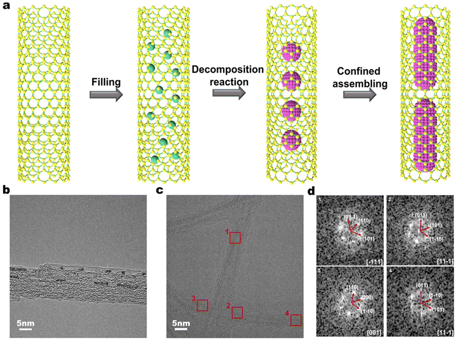
It is very important and challenging to fabricate SWCNT nanoreactors with uniform diameters and lengths. We developed a defect-induced cutting method for the controllable and efficient preparation of c-SWCNTs, as shown in Fig. 1. Defects are generated on the walls of SWCNTs through H2 plasma treatment (Fig. 1a and b). A kinetically controlled gas etching reaction was subsequently performed to cut the SWCNTs preferentially at defect sites (Fig. 1b and c). Furthermore, the defect density can be tuned by varying the plasma power and processing time. Improving the yield of c-SWCNTs (cutting efficiency) is another tough task. H2O vapor with appropriate chemical reactivity was selected as a mild etchant to react with SWCNTs at defect sites and acts as a gentle “knife” to cut the SWCNTs into segments. Since the reaction is kinetically controlled, c-SWCNT nanoreactors (Fig. 1d) with different lengths can be obtained by changing the reaction temperature and H2O vapor concentration. There is a balance between the length and yield of c-SWCNTs, which mainly depends on the etching reaction conditions. Uniform c-SWCNT nanoreactors would be fabricated efficiently by optimizing the conditions of plasma treatment and the H2O etching reaction. | ||
| Fig. 1 Schematic illustration of the fabrication of SWCNT nanoreactors. (a and b) Generation of defects on the walls of SWCNTs by H2 plasma treatment. (b and c) Cutting of SWCNTs into segments at the defect sites by H2O etching. (c and d) Filling of the c-SWCNT nanoreactors with foreign substances. | ||
The morphologies of the initial SWCNTs and c-SWCNTs were characterized using AFM, SEM, and TEM. As shown in the AFM images (Fig. 2a and b), the original SWCNTs are randomly dispersed on the substrate. SEM and TEM observations show that (Fig. S1a and b†) high-density SWCNT networks are formed, and most tubes are isolated. Bundled SWCNTs were dispersed on the substrate so that the tube walls can be fully exposed and accessed by the etchant. Furthermore, the dispersed SWCNTs have clean and straight walls before cutting, which indicates their high quality. The mean length of the initial SWCNTs is determined to be 1.4 μm by measuring 200 tubes using AFM (Fig. 2c). After cutting, the resulting c-SWCNTs are much shorter (Fig. 2b, Fig. S1b†) in length. Most adjacent short tubes have the same orientation, indicating that one original long tube has been cut into several segments. Based on AFM characterization, the length distribution of the c-SWCNTs is shown in Fig. 2d, where most SWCNTs have lengths in the range of 50–300 nm, and the average length is calculated to be 175 nm under the optimized conditions. In addition, we tried to assess the yield by measuring the length and the area density before and after cutting. The yield is calculated to be 75% (for details see the ESI†) when the average length of the c-SWCNTs is 175 nm, which is higher than most published results.20,42 However, some long SWCNTs are also observed, which can be attributed to the presence of SWCNT bundles. Furthermore, due to the resolution limitation of AFM characterization, some ultrashort c-SWCNTs were not detected, and the yield could be even higher than the calculated results.
 | ||
| Fig. 2 Morphologies of the original SWCNTs and c-SWCNTs. AFM images of the (a) initial SWCNTs and (b) c-SWCNTs. Length distributions of the (c) original and (d) c-SWCNTs measured by AFM. | ||
3.2 Effect of defect introduction on the efficient cutting of SWCNTs
Comparative experiments were conducted to reveal the defect-induced gas etching mechanism. When air plasma treatment was performed to generate defects, no SWCNTs were left after the H2O vapor etching. This is because too many defects are introduced into the walls of the SWCNTs by air plasma treatment with high chemical reactivity, and all the SWCNTs are removed by the following H2O vapor etching. Without plasma treatment, the morphology of the c-SWCNTs obtained after H2O vapor etching is shown in Fig. S2a.† We can see that both long and short SWCNTs are randomly dispersed on the substrate. The lengths of the c-SWCNTs distribute in a wide range of 50–650 nm (Fig. S2b†), and the mean value is 334 nm, which is much longer than that of the sample that underwent H2 plasma treatment.The power of plasma may also influence the generation of defects on the SWCNTs significantly. We tuned the power of plasma applied in the range of 5–20 W. With the increase of plasma power, the G/D ratios of the SWCNTs decrease dramatically (Fig. S3a†), indicating that more defects are introduced. After H2O vapor etching, the SWCNTs’ density also decreased apparently (Fig. S4a–c†). This indicates that more SWCNTs were removed during the H2O etching process. The change in the mean length of the c-SWCNTs is not obvious when higher-power H2 plasma treatment is performed (Fig. S4d–f†). However, few c-SWCNTs with the same orientation are observed (Fig. S4a–c†), indicating that too many defects lead to serious destruction and loss of SWCNTs. To balance the cutting and yield of the c-SWCNTs, a low power of 5 W H2 plasma was selected.
Other than H2 plasma power, the treatment time also affects the generation of defects. We prolonged the time of plasma treatment from 30 s to 120 s with a power of 5 W and found that the G/D ratio of the SWCNTs decreased obviously (Fig. S3b†). Fig. 3a–c show the morphology of the c-SWCNTs obtained with different H2 plasma treatment times. Most adjacent segments have the same orientation, suggesting that each SWCNT is cut into several parts. The lengths of the c-SWCNTs are mainly distributed in the range of 50–350 nm (Fig. 3d–f). The mean lengths of the c-SWCNTs obtained through 60 s, 90 s, and 120 s of plasma treatment are 150 nm, 125 nm, and 125 nm, respectively. However, the yield decreased when a longer plasma treatment time was used. The plasma treatment time was finally optimized as 90 s for defect introduction.
 | ||
| Fig. 3 AFM images and length distributions of the c-SWCNTs obtained by (a and d) 60 s, (b and e) 90 s, and (c and f) 120 s H2 plasma treatment. The average lengths of c-SWCNTs are (a) 150 nm, (b) 125 nm, and (c) 125 nm. | ||
3.3 Effects of H2O etching on the controlled cutting of SWCNTs
After defect generation by H2 plasma, H2O vapor would prefer to adsorb at the defect sites and react with the SWCNTs to achieve cutting. To investigate the adsorption site of H2O, first-principles calculations based on density functional theory implemented in the Vienna ab initio simulation package (VASP)44,45 with the projector augmented wave (PAW)46,47 method and the Perdew–Burke–Erzenhof (PBE)48 exchange–correlation functional were adopted and performed. 27 × 27 × 25.37 Å3 supercells were used to simulate the SWCNT pristine surface, which contained 4 carbon vacancies, and H2O molecules were then placed on the defect or perfect surface (Fig. 4). One-dimensional periodic boundary conditions were used along the tube axis to simulate infinitely long nanotube systems, and the length in this direction is 25.37 Å which is sufficient to prevent interactions between the periodic images. Along the remaining two non-periodic directions, a vacuum region of ∼18 Å was taken into consideration. Using the conjugate-gradient algorithm, the atomic positions in the supercell were completely relaxed without any restrictions, and the convergence threshold was set at 10−5 eV for the total energy and 10−2 eV Å−1 for the force on each atom. Gaussian smearing of 0.2 eV was employed. The valence states of C (2s22p2), H (1s1), and O (2s22p4) were considered for the construction of the corresponding pseudopotential. We investigated the adsorption site of H2O using the following formula,| ΔE = Edefect − Eperfect |
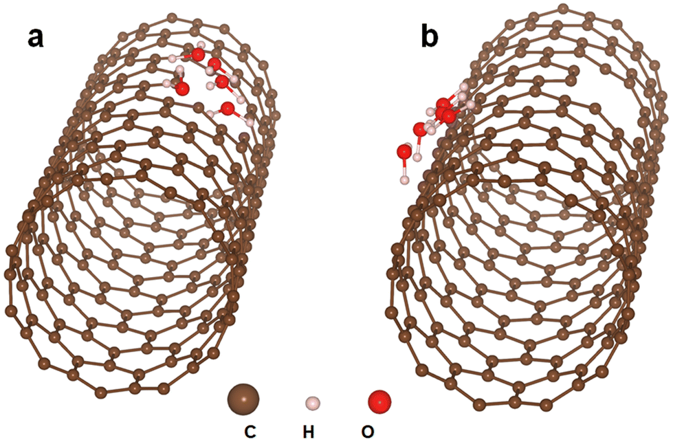 | ||
| Fig. 4 First-principles calculations of H2O adsorption on the (a) defects of SWCNTs and (b) walls of SWCNTs without defects. | ||
As a typical etchant, H2O has been used to react with amorphous carbon and metallic SWCNTs to synthesize high-purity SWCNT forests49 and high-quality semiconducting SWCNTs.50,51 Zhang et al. found that the H2O etchant has good selectivity for obtaining SWCNTs with different chiralities.52 H2O is able to react with amorphous carbon and SWCNTs under appropriate conditions.53 Several studies have demonstrated that sp3 carbon has higher chemical activity than sp2 carbon,54 and the defects located in the walls of carbon nanotubes would adsorb and react with H2O in advance.55,56 The defect sites at the carbonaceous surface dissociate the incoming water molecules, leading to a continuous reaction.57 Furthermore, the reaction of H2O and carbon is kinetically controllable by tuning the temperature, H2O concentration, and reaction time. To efficiently obtain short SWCNTs with a narrow length distribution, the conditions of the H2O etching reaction were investigated using the original SWCNTs. The AFM images of the c-SWCNTs obtained by optimizing the H2O etching reaction temperature in the range of 750–780 °C, and their corresponding statistical length distributions are shown in Fig. S5.† Shorter SWCNTs were observed when the temperature was increased. However, almost no short c-SWCNTs with the same orientation were observed at 780 °C (Fig. S5c†), indicating that some of the SWCNTs were removed. It is also confirmed that the etching reaction starts from the ends of the SWCNTs. Too high a reaction temperature would result in a low yield of c-SWCNTs.
The etching reaction is kinetically controlled, and the reactant concentration plays an important role. The concentration of H2O was tuned in the range of 1000–2000 ppm. As shown in Fig. S6,† the length becomes shorter with the increase of H2O concentration. Most SWCNTs are less than 200 nm in length (Fig. S6e and f†). However, the density dropped obviously and only 10 tubes were observed in the AFM image when the H2O concentration was 2000 ppm. A large number of nanoparticles were observed after H2O etching with a high concentration of H2O (Fig. S6b and c†), indicating the presence of ultra-short SWCNTs. However, SWCNTs with lengths shorter than 50 nm could not be observed due to the resolution limitation of AFM characterization. Although much shorter SWCNTs can be obtained with higher concentrations of the etchant, the yield of c-SWCNTs is too low. The H2O etching reaction is kinetically controlled, and the reactant concentration severely affects the reaction rate. To efficiently cut SWCNTs, a relatively low concentration of H2O is preferred.
As a kinetics-controlled reaction, the etching time plays an important role in the efficient cutting of SWCNTs. As shown in Fig. S7,† 5 min is the optimized time for efficiently cutting SWCNTs with a narrow length distribution. As can be seen in Fig. S7a and d,† long SWCNTs were obtained after H2O etching at 750 °C for 4 min, and the average length is about 250 nm. Upon prolonging the etching time, as shown in Fig. S7c and f,† 30% of SWCNTs have lengths shorter than 100 nm, and few of them have the same orientation. Also, the density of short SWCNTs decreases obviously, indicating that some SWCNTs are removed by H2O.
3.4 Filling of c-SWCNT nanoreactors
c-SWCNTs were used as nanoreactors to prepare WO3 nanoparticles and ultrathin nanowires. As shown in Fig. 5a, C9H12W(CO)3 was used as a precursor and the c-SWCNTs were filled with it by a low-pressure CVD method. Then, the precursor decomposed at an increased temperature, and WO3 nanoparticles (Fig. 5b) or ultrathin nanowires were formed in the hollow core of the SWCNTs (Fig. 5c). We measured the size of the WO3 nanowires by TEM observation. As shown in Fig. S8,† the length of the WO3 nanowires mainly distributes in the range of 7–14 nm, and their diameters are in the range of 1.0–1.6 nm, showing good structural uniformity. Compared to previous reports, the filling efficiency is significantly improved due to the reduced length of the c-SWCNTs, and long WO3 nanowires are observed to fill the inside of the hollow core of the SWCNTs.58 The fast Fourier transform (FFT) diffraction patterns of the nanowires shown in Fig. 5c are used to assign the lattice fringes. As shown in Fig. 5d, the identified patterns are in good agreement with the spacings of (−1 1 1), (1 1 −1), and (0 0 1) crystal planes of WO3, suggesting that the W/O elemental composition of the nanowires is 1![[thin space (1/6-em)]](https://www.rsc.org/images/entities/char_2009.gif) :3.
:3.
 | ||
| Fig. 5 Preparation of nanoparticles and nanowires in SWCNT nanoreactors. (a) Schematic showing the preparation of WO3 nanostructures in SWCNT nanoreactors. (b) TEM image of WO3 nanoparticles@SWCNTs. (c) TEM images of long ultrathin WO3 nanowires@SWCNTs. (d) FFT patterns of the marked areas in (c) and their lattice fringes. | ||
To evaluate the radiation resistance of the WO3 nanowires encapsulated in the chamber of SWCNTs, electron diffraction was performed under TEM while maintaining the electron dose at 2.84 × 10⁶ eV nm−2 s−1. After 120 s of electron beam irradiation, the WO3 nanocrystals retain well while the walls of the SWCNTs start to degrade (Fig. 6a and b), suggesting a high electron irradiation tolerance of the WO3 nanowires@SWCNT hybrid. On the other hand, the crystal face of the WO3 nanowires supported on the walls of the SWCNTs changed from (1 1 1) to (4 0 0) after undergoing similar 120 s electron beam irradiation (Fig. 6c and d). Because SWCNTs have good electrical conductivity, electrons can be transferred through the walls of carbon nanotubes, and WO3 cylinder-shaped nanowires encapsulated in SWCNTs have superior electron radiation resistance. For the WO3 nanowires@SWCNTs, the tube wall with good electrical conductivity and electron radiation durability functions as a protective shell. Therefore, the defect-induced H2O etching method is efficient for fabricating SWCNT nanoreactors, providing a way for synthesizing SWCNT-based derivatives with intriguing properties.
 | ||
| Fig. 6 Electron radiation resistance of WO3 nanowires@SWCNTs. TEM images of WO3 nanowires@SWCNTs (a) before and (b) after electron beam irradiation. TEM images of WO3 nanowires supported on SWCNTs (c) before and (d) after electron beam irradiation. | ||
4. Conclusions
In conclusion, an efficient and controllable cutting of SWCNTs is achieved by combining H2 plasma treatment and H2O vapor etching. Long SWCNTs were cut into segments with an average length of 175 nm, and the yield was about 75% under the optimum conditions. The resulting c-SWCNTs have both high crystallinity and short lengths and can be used as nanoreactors with ultrasmall confined space. The c-SWCNT nanoreactors with a short diffusion path were efficiently filled with WO3 nanoparticles and nanowires. The WO3 nanowires encapsulated in the c-SWCNTs show high electron irradiation tolerance. This offers guidance for the design and preparation of SWCNT-based derivatives with excellent properties.Author contributions
Conceptualization – XZ, FZ, and CL; data curation – XZ, ZZ, and FZ; formal analysis – XZ, ZZ, GZ, MZ, and FZ; funding acquisition – FZ, HMC, and CL; investigation – XZ, ZZ, GZ, MZ, FZ, and CL; methodology – FZ, PXH, CS, HMC, MW, and CL; project – FZ, MW, and CL; resources – FZ, HMC, and CL; software – GZ; supervision – FZ, MW, PXH, CS, and CL; validation – XZ, ZZ, and FZ; visualization – XZ, ZZ, GZ, and FZ; writing of the original draft – XZ, FZ, and CL; writing – review & editing – all authors.Conflicts of interest
The authors declare no conflict of interest.Acknowledgements
This work was supported by the National Natural Science Foundation of China (grants 52072376, 52130209, and 51702325), the Nature Science Foundation of Liaoning Province (grant 2022-MS-012), the CAS/SAFEA International Partnership Program for Creative Research Teams, and the Liaoning BaiQianWan Talents.References
- G. Hills, C. Lau, A. Wright, S. Fuller, M. D. Bishop, T. Srimani, P. Kanhaiya, R. Ho, A. Amer, Y. Stein, D. Murphy, A. A. Chandrakasan and M. M. Shulaker, Nature, 2019, 572, 595–602 CrossRef CAS PubMed.
- L. J. Liu, J. Han, L. Xu, J. S. Zhou, C. Y. Zhao, S. J. Ding, H. W. Shi, M. M. Xiao, L. Ding, Z. Ma, C. H. Jin, Z. Y. Zhang and L. M. Peng, Science, 2020, 368, 850–856 CrossRef CAS PubMed.
- J. Geng, K. Kim, J. Zhang, A. Escalada, R. Tunuguntla, L. R. Comolli, F. I. Allen, A. V. Shnyrova, K. R. Cho, D. Munoz, Y. M. Wang, C. P. Grigoropoulos, C. M. Ajo-Franklin, V. A. Frolov and A. Noy, Nature, 2014, 514, 612–615 CrossRef CAS PubMed.
- S. Y. Yang, Z. W. Wang, Y. H. Ping, Y. Y. Miaol, Y. M. Xiao, L. B. Qu, L. Zhang, Y. S. Hu and J. S. Wang, Beilstein J. Nanotechnol., 2020, 11, 1728–1741 CrossRef CAS PubMed.
- S. Z. M. Madani, M. M. Safaee, M. Gravely, C. Silva, S. Kennedy, G. D. Bothun and D. Roxbury, ACS Appl. Nano Mater., 2021, 4, 331–342 CrossRef CAS.
- B. S. Wong, S. L. Yoong, A. Jagusiak, T. Panczyk, H. K. Ho, W. H. Ang and G. Pastorin, Adv. Drug Delivery Rev., 2013, 65, 1964–2015 CrossRef CAS PubMed.
- X. L. Pan and X. H. Bao, Acc. Chem. Res., 2011, 44, 553–562 CrossRef CAS PubMed.
- J. P. Xiao, X. L. Pan, S. J. Guo, P. J. Ren and X. H. Bao, J. Am. Chem. Soc., 2015, 137, 477–482 CrossRef CAS PubMed.
- J. T. W. Wang, R. Klippstein, M. Martincic, E. Pach, R. Feldman, M. Sefl, Y. Michel, D. Asker, J. K. Sosabowski, M. Kalbac, T. Da Ros, C. Menard-Moyon, A. Bianco, I. Kyriakou, D. Emfietzoglou, J. C. Saccavini, B. Ballesteros, K. T. Al-Jamal and G. Tobias, ACS Nano, 2020, 14, 129–141 CrossRef CAS PubMed.
- H. Zare, S. Ahmadi, A. Ghasemi, M. Ghanbari, N. Rabiee, M. Bagherzadeh, M. Karimi, T. J. Webster, M. R. Hamblin and E. Mostafavi, Int. J. Nanomed., 2021, 16, 1681–1706 CrossRef PubMed.
- J. T. W. Wang, C. Spinato, R. Klippstein, P. M. Costa, M. Martincic, E. Pach, A. P. R. de Garibay, C. Menard-Moyon, R. Feldman, Y. Michel, M. Sefl, I. Kyriakou, D. Emfietzoglou, J. C. Saccavini, B. Ballesteros, G. Tobias, A. Bianco and K. T. Al-Jamal, Carbon, 2020, 162, 410–422 CrossRef CAS.
- M. Hart, J. Chen, A. Michaelides, A. Sella, M. S. P. Shaffer and C. G. Salzmann, Inorg. Chem., 2019, 58, 15216–15224 CrossRef CAS PubMed.
- M. Hart, E. R. White, J. Chen, C. M. McGilvery, C. J. Pickard, A. Michaelides, A. Sella, M. S. P. Shaffer and C. G. Salzmann, Angew. Chem., Int. Ed., 2017, 56, 8144–8148 CrossRef CAS PubMed.
- R. J. Kashtiban, M. G. Burdanova, A. Vasylenko, J. Wynn, P. V. C. Medeiros, Q. Ramasse, A. J. Morris, D. Quigley, J. Lloyd-Hughes and J. Sloan, ACS Nano, 2021, 15, 13389–13398 CrossRef CAS PubMed.
- J. Y. Zhang, C. C. Fu, S. X. Song, H. C. Du, D. Zhao, H. Y. Huang, L. H. Zhang, J. Guan, Y. F. Zhang, X. L. Zhao, C. S. Ma, C. L. Jia and D. Tomanek, Nano Lett., 2020, 20, 1280–1285 CrossRef CAS PubMed.
- C. A. Slade, A. M. Sanchez and J. Sloan, Nano Lett., 2019, 19, 2979–2984 CrossRef CAS PubMed.
- J. Deng, P. J. Ren, D. H. Deng, L. Yu, F. Yang and X. H. Bao, Energy Environ. Sci., 2014, 7, 1919–1923 RSC.
- Q. Q. He, T. F. Xu, J. J. Li, J. L. Wang, C. Q. Jin, Q. Chen, X. K. Gu, X. G. Wang, J. T. Wei, H. P. Duan and Y. J. Gong, Adv. Energy Mater., 2022, 12, 202200849 Search PubMed.
- S. M. Jin, P. Wijesekara, P. D. Boyer, K. N. Dahl and M. F. Islam, J. Mater. Chem. B, 2017, 5, 6657–6665 RSC.
- W. Q. Dai and D. Z. Wang, J. Phys. Chem. C, 2021, 125, 9593–9617 CrossRef CAS.
- N. Rubio, C. Fabbro, M. A. Herrero, A. de la Hoz, M. Meneghetti, J. L. G. Fierro, M. Prato and E. Vazquez, Small, 2011, 7, 665–674 CrossRef CAS PubMed.
- N. Pierard, A. Fonseca, Z. Konya, I. Willems, G. Van Tendeloo and J. B. Nagy, Chem. Phys. Lett., 2001, 335, 1–8 CrossRef CAS.
- A. Kukovecz, T. Kanyo, Z. Konya and I. Kiricsi, Carbon, 2005, 43, 994–1000 CrossRef CAS.
- S. R. Lustig, E. D. Boyes, R. H. French, T. D. Gierke, M. A. Harmer, P. B. Hietpas, A. Jagota, R. S. McLean, G. P. Mitchell, G. B. Onoa and K. D. Sams, Nano Lett., 2003, 3, 1007–1012 CrossRef CAS.
- T. M. D. Alharbi, K. Vimalanathan, I. K. Alsulami and C. L. Raston, Nanoscale, 2019, 11, 21394–21403 RSC.
- S. R. Wang, Z. Y. Liang, B. Wang, C. Zhang and Z. Rahman, Nanotechnology, 2007, 18, 6 Search PubMed.
- H. Xu, H. Abe, M. Naito, Y. Fukumori, H. Ichikawa, S. Endoh and K. Hata, Adv. Powder Technol., 2010, 21, 551–555 CrossRef CAS.
- M. S. Raghuveer, P. G. Ganesan, J. D'Arcy-Gall, G. Ramanath, M. Marshall and I. Petrov, Appl. Phys. Lett., 2004, 84, 4484–4486 CrossRef CAS.
- F. Banhart, J. X. Li and M. Terrones, Small, 2005, 1, 953–956 CrossRef CAS PubMed.
- Y. Wang, L. Gao, J. Sun, Y. Q. Liu, S. Zheng, H. Kajiura, Y. M. Li and K. Noda, Chem. Phys. Lett., 2006, 432, 205–208 CrossRef CAS.
- M. V. Shuba, A. G. Paddubskaya, P. P. Kuzhir, S. A. Maksimenko, V. K. Ksenevich, G. Niaura, D. Seliuta, I. Kasalynas and G. Valusis, Nanotechnology, 2012, 23, 9 CrossRef PubMed.
- M. Wisniewski, A. P. Terzyk, Y. Hattori, K. Kaneko, F. Okino and B. Kruszka, Chem. Phys. Lett., 2009, 482, 316–319 CrossRef CAS.
- J. Y. Xie, M. N. Ahmad, H. D. Bai, H. Y. Li and W. T. Yang, Sci. China: Chem., 2010, 53, 2026–2032 CrossRef CAS.
- Z. Gu, H. Peng, R. H. Hauge, R. E. Smalley and J. L. Margrave, Nano Lett., 2002, 2, 1009–1013 CrossRef CAS.
- M. Q. Tran, C. Tridech, A. Alfrey, A. Bismarck and M. S. P. Shaffer, Carbon, 2007, 45, 2341–2350 CrossRef CAS.
- S. A. Miners, G. A. Rance, A. La Torre, S. M. Kenny and A. N. Khlobystov, J. Mater. Chem. C, 2014, 2, 8357–8363 RSC.
- A. La Torre, G. A. Rance, S. A. Miners, C. H. Lucas, E. F. Smith, M. W. Fay, T. Zoberbier, M. C. Gimenez-Lopez, U. Kaiser, P. D. Brown and A. N. Khlobystov, Nanotechnology, 2016, 27, 8 CrossRef PubMed.
- Z. Y. Chen, K. J. Ziegler, J. Shaver, R. H. Hauge and R. E. Smalley, J. Phys. Chem. B, 2006, 110, 11624–11627 CrossRef CAS PubMed.
- M. H. Li, M. Boggs, T. P. Beebe and C. P. Huang, Carbon, 2008, 46, 466–475 CrossRef CAS.
- K. J. Ziegler, Z. N. Gu, J. Shaver, Z. Y. Chen, E. L. Flor, D. J. Schmidt, C. Chan, R. H. Hauge and R. E. Smalley, Nanotechnology, 2005, 16, S539–S544 CrossRef PubMed.
- W. S. Zhang, Y. T. Liu, T. T. Yao, G. P. Wu and Q. F. Liu, J. Phys. Chem. C, 2020, 124, 27097–27106 CrossRef CAS.
- Y. F. Li, X. J. Wu, M. Kim, J. Fortner, H. R. Qu and Y. H. Wang, Chem. Mater., 2019, 31, 4536–4544 CAS.
- Y. Tian, N. Wei, P. Laiho, S. Ahmad, Y. Magnin, Y. P. Liao, C. Bichara, H. Jiang and E. I. Kauppinen, Carbon, 2019, 143, 481–486 CrossRef CAS.
- J. Furthmuller, J. Hafner and G. Kresse, Phys. Rev. B: Condens. Matter Mater. Phys., 1994, 50, 15606–15622 CrossRef PubMed.
- G. Kresse and J. Furthmuller, Phys. Rev. B: Condens. Matter Mater. Phys., 1996, 54, 11169–11186 CrossRef CAS PubMed.
- P. E. Blochl, Phys. Rev. B: Condens. Matter Mater. Phys., 1994, 50, 17953–17979 CrossRef PubMed.
- G. Kresse and D. Joubert, Phys. Rev. B: Condens. Matter Mater. Phys., 1999, 59, 1758–1775 CrossRef CAS.
- J. P. Perdew, K. Burke and M. Ernzerhof, Phys. Rev. Lett., 1996, 77, 3865–3868 CrossRef CAS PubMed.
- K. Hata, D. N. Futaba, K. Mizuno, T. Namai, M. Yumura and S. Iijima, Science, 2004, 306, 1362–1364 CrossRef CAS PubMed.
- W. W. Zhou, S. T. Zhan, L. Ding and J. Liu, J. Am. Chem. Soc., 2012, 134, 14019–14026 CrossRef CAS PubMed.
- F. Yang, X. Wang, J. Si, X. L. Zhao, K. Qi, C. H. Jin, Z. Y. Zhang, M. H. Li, D. Q. Zhang, J. Yang, Z. Y. Zhang, Z. Xu, L. M. Peng, X. D. Bai and Y. Li, ACS Nano, 2017, 11, 186–193 CrossRef CAS PubMed.
- Z. Q. Wang, Q. C. Zhao, L. M. Tong and J. Zhang, J. Phys. Chem. C, 2017, 121, 27655–27663 CrossRef CAS.
- D. C. Shi, W. D. Tennyson, J. C. Keay, E. S. Sanchez, M. B. Johnson and D. E. Resasco, Chem. Phys. Lett., 2012, 525–26, 82–86 CrossRef.
- J. L. Rivera, J. L. Rico and F. W. Starr, J. Phys. Chem. C, 2007, 111, 18899–18905 CrossRef CAS.
- M. D. Ellison, A. P. Good, C. S. Kinnaman and N. E. Padgett, J. Phys. Chem. B, 2005, 109, 10640–10646 CrossRef CAS PubMed.
- P. Kim, Y. J. Zheng and S. Agnihotri, Ind. Eng. Chem. Res., 2008, 47, 3170–3178 CrossRef CAS.
- M. Oubal, S. Picaud, M. T. Rayez and J. C. Rayez, Surf. Sci., 2010, 604, 1666–1673 CrossRef CAS.
- T. T. Cui, X. L. Pan, J. H. Dong, S. Miao, D. Y. Miao and X. H. Bao, Nano Res., 2018, 11, 3132–3144 CrossRef CAS.
Footnotes |
| † Electronic supplementary information (ESI) available. See DOI: https://doi.org/10.1039/d2nr06696c |
| ‡ These authors contributed equally to this work. |
| This journal is © The Royal Society of Chemistry 2023 |