
 Open Access Article
 This Open Access Article is licensed under a Creative Commons Attribution-Non Commercial 3.0 Unported Licence
Observation of the photovoltaic effect in a van der Waals heterostructure†
Shaochun
Zhang
a,
Mina
Maruyama
b,
Susumu
Okada
b,
Mengsong
Xue
a,
Kenji
Watanabe
 d,
Takashi
Taniguchi
c,
Kazuki
Hashimoto
e,
Yasumitsu
Miyata
e,
Ruben
Canton-Vitoria
a and
Ryo
Kitaura
*ac
d,
Takashi
Taniguchi
c,
Kazuki
Hashimoto
e,
Yasumitsu
Miyata
e,
Ruben
Canton-Vitoria
a and
Ryo
Kitaura
*ac
aDepartment of Chemistry, Nagoya University, Nagoya, Aichi 464-8602, Japan. E-mail: KITAURA.Ryo@nims.go.jp; r.kitaura@nagoya-u.jp
bDepartment of Physics, Graduate School of Pure and Applied Sciences, University of Tsukuba, 1-1-1 Tennodai, Tsukuba 305-8571, Japan
cInternational Center for Materials Nanoarchitectonics, National Institute for Materials Science, 1-1 Namiki, Tsukuba 305-0044, Japan
dResearch Center for Functional Materials, National Institute for Materials Science, 1-1 Namiki, Tsukuba 305-0044, Japan
eDepartment of Physics, Tokyo Metropolitan University, Hachioji, Tokyo 192-0397, Japan
First published on 20th February 2023
Abstract
van der Waals (vdW) heterostructures, which can be assembled with various two-dimensional materials, provide a versatile platform for exploring emergent phenomena. Here, we report an observation of the photovoltaic effect in a WS2/MoS2 vdW heterostructure. Light excitation of WS2/MoS2 at a wavelength of 633 nm yields a photocurrent without applying bias voltages, and the excitation power dependence of the photocurrent shows characteristic crossover from a linear to square root dependence. Photocurrent mapping has clearly shown that the observed photovoltaic effect arises from the WS2/MoS2 region, not from Schottky junctions at electrode contacts. Kelvin probe microscopy observations show no slope in the electrostatic potential, excluding the possibility that the photocurrent originates from an unintentionally formed built-in potential.
Introduction
Artificial van der Waals stackings (vdWSs)1–3 provide a general platform to explore emergent phenomena. Unlike fabricating conventional heterostructures based on three-dimensional materials, stacking different two-dimensional (2D) materials can realize diverse vdWSs regardless of the lattice mismatch. The interlayer interactions in vdWSs can cause synergistic effects in the electronic and optical properties, which are absent in the individual components alone. For example, twisted bilayer graphene with a twist angle of ∼1.1°, the so-called magic angle,4 exhibits unconventional superconductivity due to the flat bands arising from the interlayer moiré potential. Also, vdWSs composed of transition metal dichalcogenides (TMDs) host long-lived interlayer excitons,5 where electrons and holes reside in different layers. Furthermore, when TMD-based vdWSs possess a certain stacking angle, moiré excitons emerge6 and work as arrayed quantum emitters.7 These emergent properties have attracted significant attention, and further discovery is yet to come.Meanwhile, the photovoltaic effect (PVE), which emerges in noncentrosymmetric materials, has ignited the search for new PVE materials. Typically, PVE appears in inhomogeneous semiconductors with p–n junctions,8 where the spontaneously formed built-in potential generates a photovoltage in response to light irradiation. In contrast, the bulk photovoltaic effect (BPVE),9 which appears in noncentrosymmetric materials,10 does not require a built-in potential. Theoretical studies have proposed the origin of BPVE:11 (1) the shift of the electron cloud in real space upon light excitation (shift current) and (2) the asymmetry of the velocity of electron wavepackets (ballistic current). As these mechanisms differ distinctly from PVE based on p–n junctions, BPVE is free from the Shockley–Queisser (SQ) limit.12 The possibility of PVE materials beyond the SQ limit and their fundamental mechanisms have been attracting much attention.
vdWSs provide a diverse platform to search for new systems with emergent properties, including non-zero BPVE. Although inversion symmetry breaking is required for BPVE to emerge, this requirement alone is insufficient. For example, the three-fold rotational (C3) symmetry of monolayer TMDs cancels out the in-plane photovoltage, resulting in zero BPVE. By contrast, significant BPVE appears in WS2 nanotubes13 and WSe2/black phosphorus (BP),14 where the C3 symmetry is broken by rolling-up and BP stacking, respectively. These examples show that lowering the spatial symmetry can cause BPVE, and stacking two independent layers to form vdWSs is a promising way to fabricate new BPVE materials.
Here we report the emergence of PVE in WS2/MoS2 vdW heterostructures. Although both WS2 and MoS2 have C3 symmetry and sets of mirror planes (Fig. 1A), the symmetry can probably be altered at the WS2 and MoS2 interface due to the interlayer interaction. Photocurrent mapping measurements have demonstrated that a photocurrent up to 28 nA appears without applying bias voltages under 996 μW light excitation; the photocurrent is almost zero when the excitation laser sport is placed outside the stacked region. The observed photocurrent is comparable to the recently reported PVE response in WS2 nanotubes13 and strained MoS2.11 Kelvin probe microscopy observations did not show any drop and/or slope in potential, ruling out the photocurrent originating from the unintentional built-in potential. The excitation power dependence of the photocurrent shows a linear relationship in the low excitation power region and a square root relationship in the high power region. This work suggests that simply stacking two different layered structures can lead to observing PVE, which is consistent with BPVE.
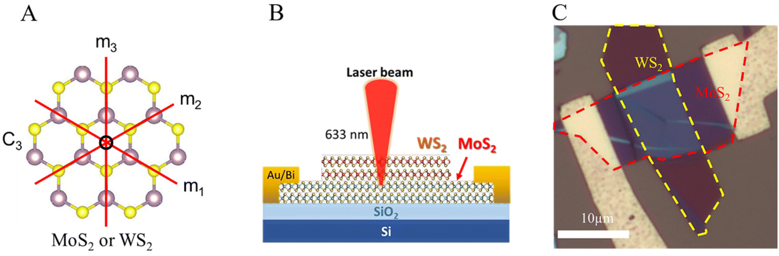 | ||
| Fig. 1 (A) Schematic illustration of the structure of monolayer MoS2 or WS2. Purple and yellow spheres correspond to metal and sulfur atoms, respectively. The red lines and the open circle represent mirror planes and the C3 axe, respectively. (B) and (C) are a schematic representation and an optical image of the WS2/MoS2 device, respectively. | ||
Results and discussion
According to the procedure reported in previous work, multilayer WS2 and MoS2 flakes were mechanically exfoliated on SiO2/Si (270 nm) substrates and transferred to form vdWSs by the dry method with polymer stamps.15 Raman spectra obtained with 532 nm excitation show the E12g and A1g peaks of WS2 and MoS2, located at 354 cm−1,421.5 cm−1 and 384 cm−1, 408.5 cm−1 respectively,16 consistent with the multilayer structure (see ESI, Fig. S1†). Also, the atomic force microscopy (AFM) image and height profile show that MoS2 is 6-layer and WS2 is 5-layer (see ESI, Fig. S2†). As for the stacking angle of vdWSs, we estimated the crystal orientation of each flake based on the edge direction: linear edges with an angle of 60 or 120 degrees corresponding to the zigzag edge.17 Once knowing the crystal orientation, we can control the stacking angle in WS2/MoS2. In this study, we use a stacking angle of 90 and 60 degrees; hereafter the results of 90 degrees are described in detail (for 60 degrees, please see the ESI†). After making vdWSs, we made electrical contact with bismuth (Bi) to reduce the Schottky barrier at each contact;18 a small Schottky barrier is essential to have low contact resistance, leading to a larger short-circuit current. It should be noted that the two Bi electrodes contact only with the MoS2 part, not the WS2/MoS2 stacking region, as shown in Fig. 1B and C.To study the spatial distribution of the photocurrent in WS2/MoS2 systemically, we applied scanning photocurrent microscopy, where an excitation laser spot is scanned across the surface of the device to measure the position dependence of the photocurrent. Fig. 2A and B (also Fig. S3A and B†) show one-dimensional and two-dimensional photocurrent mapping measured without applying a bias voltage (short-circuit current), respectively. The short-circuit current gives an opposite sign at the two electrodes, consistent with the current driven by the built-in potential arising from the Schottky barriers19,20 at the contacts (or the photothermoelectric effect21,22). Also, we observed a short-circuit photocurrent with opposite signs on both edges of the WS2/MoS2 region. The photocurrent on both edges probably arises from the band bending at the lateral interface between MoS2 and WS2/MoS2.23 The orbital hybridization between WS2 and MoS2 changes the electronic bands of MoS2 only in the WS2/MoS2 region, resulting in band bending at the interface. Similar photocurrent signals were also observed in other heterostructures, such as graphene/MoS224 (Fig. S3C and D†).
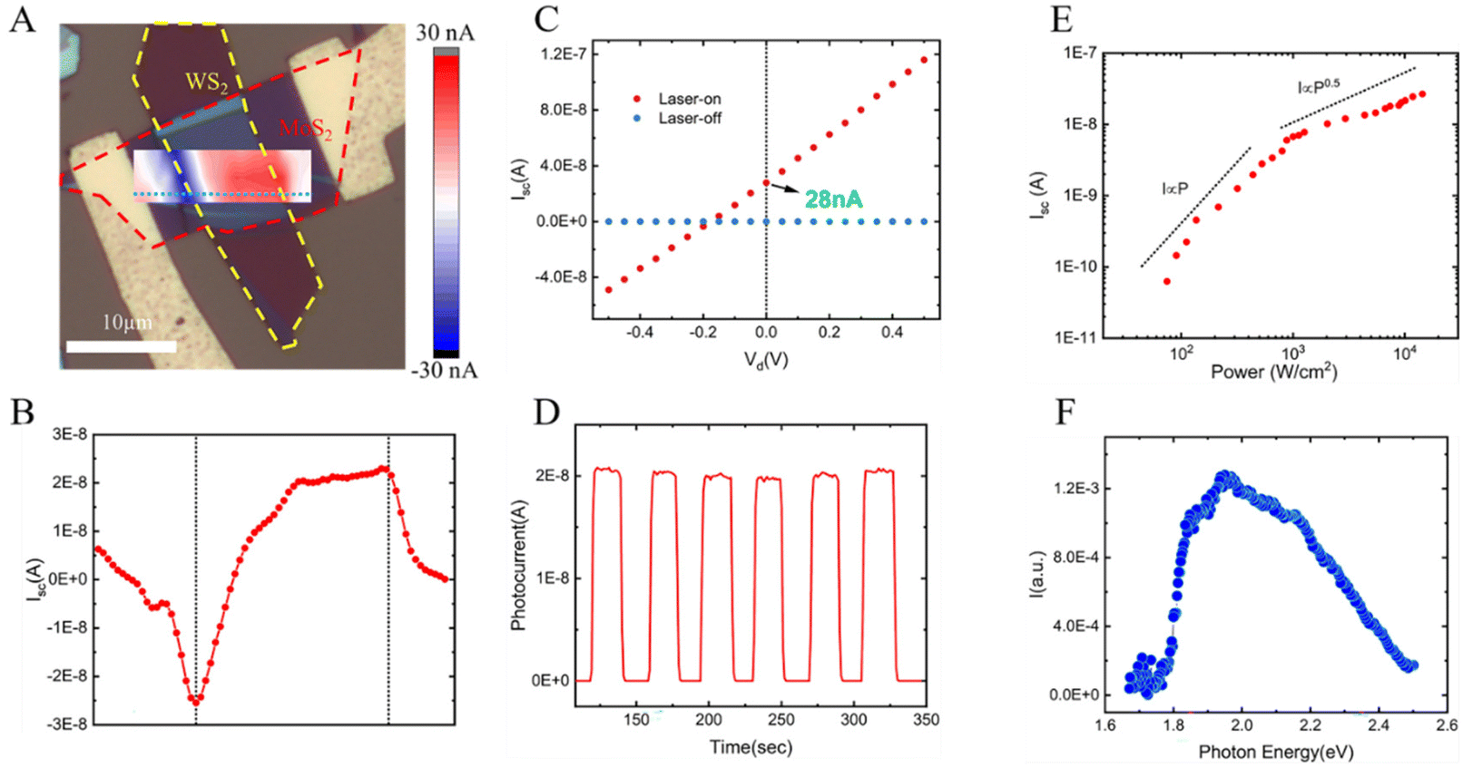 | ||
| Fig. 2 (A) A photocurrent map of the WS2/MoS2 device. (B) A photocurrent profile along the dotted line shown in (A). The black dotted lines represent the edges of the WS2. (C) I–V characteristic of the WS2/MoS2 device measured with (red) and without (blue) an excitation wavelength of 633 nm. (D) Time dependence of the photocurrent recorded during on–off cycles of an incident laser. (E) Excitation power (P) dependence of the photocurrent (I). (F) Photon energy dependence of the photocurrent. All measurements were performed at room temperature, respectively. | ||
In addition to the edges, the non-zero photocurrent also appears over the whole WS2/MoS2 region. Importantly, the photocurrent is almost zero when the excitation laser spot is placed on the MoS2 part, demonstrating that the photocurrent originates from the WS2/MoS2 stacking structure. To further investigate the PVE observed at WS2/MoS2, the current–voltage (I–V) characteristics at room temperature were measured under 9.96 × 10² μW excitation with a wavelength of 633 nm. As shown in Fig. 2C, the I–V curve is linear over −0.5 to 0.5 V without any rectification behavior, which is usually seen in p–n junctions.25 The photocurrent observed without applying a voltage is 28 nA (6 × 101 A cm−2 with excitation of ∼104 W cm−2), which is considerably larger than photoresponses reported in inorganic ferroelectrics (such as BiFeO3 and BiTiO3)26–30 and comparable to the recently reported photoresponses in low-dimensional systems, such as WS2 nanotubes13 and strained MoS2.11 In contrast to the I–V curve under photoexcitation, the dark I–V curve in Fig. 2C shows almost zero throughout the voltage range tested, demonstrating that the observed current originates from photoexcitation. Fig. 2D shows the photocurrent response when the laser excitation is repeatedly turned on and off. As seen in Fig. 2D, the photocurrent returns to similar values each time the laser is turned on, indicating that the PVE in WS2/MoS2 is robust both in quality and quantity; the zero-photocurrent observed without light excitation is consistent with the zero-current shown in the dark I–V curve shown in Fig. 2C.
Fig. 2E shows a log–log plot of an excitation power dependence of the photocurrent measured with the excitation wavelength of 633 nm, showing the characteristic crossover from a linear to square-root dependence31 at around 103 μW cm−2. A similar crossover from a linear to square-root dependence has also been observed in WS2 nanotubes13 and WSe2/BP,14 where the non-zero short-circuit current originates from the shift current. To further address the mechanism of the photocurrent, we analysed the excitation wavelength dependence of the photocurrent. As seen in Fig. 2F, the wavelength dependence has several peaks in the range of 1.85–2.05 eV, which correspond to the exciton resonances of MoS2, indicating that exciton resonances can enhance the photovoltaic response; the photocurrent enhancement at exciton resonances has been predicted.32 When the photon energy increases and reaches ca. 1.8 eV, the optical gap of MoS2, the photovoltaic response is enhanced due to the increase of joint density of states and reaches the maximum around the optical transition between bands around K (K′) points. As the excitation photon energy further increases, the photovoltaic response is eventually suppressed, probably because of the reduction of the shift vector.14
Kelvin Probe Force Microscopy (KPFM) has provided critical information to exclude the possibility that the observed photocurrent arises from the unintentionally-formed built-in potential. Note that an out-of-plane built-in potential, which cannot be observed with KPFM, is probably present due to the type-II band alignment, but this built-in potential should not contribute to the lateral photocurrent observed (see also discussion in the ESI†). Fig. 3A and B illustrate a KPFM image and a line profile along the red dashed line in the image, respectively. As seen in Fig. 3B, there is no potential drop over the whole surface of the WS2/MoS2 region, clearly demonstrating that the observed photocurrent does not arise from the built-in potential; the open-circuit voltage shown in Fig. 2C means that an in-plane built-in potential of the order of 102 mV should exist if the built-in potential is the origin of the photocurrent. Note that shunt resistances alter open-circuit voltages, but it is safe to say that the actual open-circuit voltage is at least 102 meV order. The absence of a built-in potential is reasonable because we made the WS2/MoS2 structure using intrinsic WS2 and MoS2 without additional doping for p–n junctions. The slight change in potential comes from edges and wrinkles, and the potential remains almost uniform in the WS2/MoS2 region, excluding the possibility that the photocurrent originates from an electric field from surface charge. These KPFM observations mean that no electric field is unintentionally formed in our current device. Polarization direction dependence (Fig. S4†) shows a small direction dependence of the photocurrent, depending on the devices used.
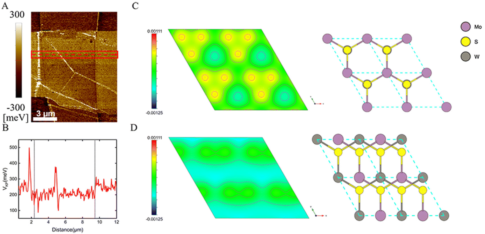 | ||
| Fig. 3 (A) Kelvin Probe Force Microscopy (KPFM) image of the WS2/MoS2 device. The image was obtained at room temperature. (B) A line profile along the red dotted line shown in (A). (C) and (D) 2D electrostatic potential profiles of AB stack WS2/MoS2 and staggered WS2/MoS2 and the corresponding structure models. The 2D profiles show electrostatic potential in the middle of the bilayer structures, representing the electrostatic potential difference between WS2/MoS2 and each component (independent monolayer MoS2 and WS2). | ||
To further explore the origin of the observed photocurrent, we have performed ab initio density functional theory (DFT) calculations of MoS2/WS2 heterostructures. We used heterostructures consisting of monolayer WS2 and MoS2 to model the interface between WS2 and MoS2 in the device; MoS2/WS2 heterostructures with different twist angles (0 and 38 degrees) and translational shifts were used. For visualizing the symmetry at the MoS2/WS2 interface, the differences in the calculated electrostatic potential between WS2/MoS2 heterostructures and isolated components are shown in Fig. 3 and Fig. S5.† As clearly seen in the contour plots, the electrostatic potential at the WS2/MoS2 interface retains the C3 rotational symmetry when the upper MoS2 and lower WS2 layers share the C3 axis. In contrast, the C3 rotational symmetry is broken when the C3 axis of each layer does not coincide. For example, in the case of the twist angle of 38 degrees, the C3 rotational symmetry disappears after a translational shift of 0.1 nm, as illustrated in Fig. 3D. This interaction-induced symmetry-breaking is similar to A/B sublattice symmetry breaking in graphene epitaxially grown on SiC.33 In this case, coupling between graphene and a SiC substrate can break the sublattice symmetry, resulting in a bandgap opening.
In the sample preparations, we manually transfer WS2 flakes onto MoS2 flakes to form WS2/MoS2, and in this case, each C3 axis probably does not match completely. As a result, the C3 symmetry breaking probably occurs at the interface. Rotational symmetry breaking by stacking has also been reported in WSe2/BP, where the interface does not possess any rotational symmetry due to distinct rotational and mirror symmetries of WSe2 and BP; two-fold and three-fold rotational symmetries of BP and WSe2 are incompatible with any rotational symmetry. On the other hand, the present MoS2/WS2 case suggests that the resulting heterostructure can break the C3 rotational symmetry, particularly at the interface, even when both components have C3 rotational symmetry. This interlayer interaction mechanism is not expected to require rigorous twist-angle and layer-number control, different from the superconductivity in twisted-bilayer graphenes,4 and indeed, we observed similar photoresponses in another WS2/MoS2 with a different twist angle and thickness (Fig. S3†).
As discussed above, the interlayer interaction may lift rotational symmetry. In TMD-based vdWSs, however, moiré lattice with C3 rotational symmetry can play an important role. In this case, the photocurrents can cancel each other out. However, the moiré periodicity is probably insufficient to cancel out the generated photocurrents, and residual currents are probably detected.34 Another possibility is that the electron–electron interaction could break symmetry spontaneously. For example, the strong interaction in twisted double bilayer graphene35 (TDBG) possesses an electronic nematic phase, where the C3 symmetry is broken. In this example, the moiré flat band plays a role and might not be dominant in misaligned WS2/MoS2 investigated in this study. The final possibility is that unintentionally introduced strain during the sample preparation breaks the C3 rotational symmetry. The process-induced strain is, however, expected to be introduced throughout the sample. In this case, both WS2/MoS2 and MoS2-only regions should show a similar photocurrent, inconsistent with the photocurrent that appears only in the WS2/MoS2 region (Fig. 2A). We, therefore, think that the process-induced strain might also not be dominant in samples investigated in this study.
Summary
The non-zero photocurrent was observed at zero bias voltage in WS2/MoS2 under photoexcitation with a wavelength of 633 nm. I–V curves under photoexcitation were linear, and the excitation power dependence showed a crossover from a linear to square root dependence. No noticeable potential drop or slope was observed in the KPFM images, which rules out the existence of unintentionally formed potential drops and slopes. DFT-based theoretical investigations suggest that spatial symmetry can be lowered due to the interlayer interaction in WS2/MoS2. These experimental results and theoretical considerations are consistent with BPVE. Although the origin of the PVEs observed in this study needs to be further explored, it provides an approach for finding materials that exhibit PVE.Experimental
Sample preparation
We prepared WS2 and MoS2 flakes by the standard mechanical exfoliation method. After selecting suitable WS2 and MoS2 flakes, WS2/MoS2 was prepared on 270 nm SiO2/Si by the polymer-based dry transfer technique. The prepared WS2/MoS2 sample was rinsed with acetone for one hour and annealed under a H2/Ar flow to clean organic residues and make contact between WS2 and MoS2 better. Finally, we made electrical contacts by the standard microfabrication technique, including pattern drawing with electron beam lithography, development of the electrode pattern, metal deposition (Au 50 nm/Bi 10 nm), and the lift-off process.Ab initio calculations
The geometrical and electronic structures were investigated using the STATE package based on DFT. A generalized gradient approximation using the Perdew–Burke–Ernzerhof functional form was employed to describe the exchange–correlation potential energy. Electron–ion interactions were treated in terms of ultrasoft pseudopotentials. The valence wave function and deficit charge density were expanded by plane-wave basis sets with cutoff energies of 25 Ry and 225 Ry, respectively. Atomic coordinates were optimized until the forces acting on each atom were less than 5 mRy A−1 under the lattice parameter corresponding to the experimental value.Measurements
All photocurrent measurements were carried out under vacuum conditions in an optical cryostat (KONTI-Cryostat-Micro, CryoVac). Helium–neon CW laser (Thorlabs, HNL050L, λ = 633 nm) was used to excite samples in photocurrent measurements, including measurements of photocurrent mapping, power dependence, I–V characteristic, and polarization dependence. For wavelength dependence measurements, a broadband super-continuum pulsed laser (SuperK EXTREME NKT Photonic, 40 MHz) with a monochromator (Princeton Instruments, SP2150) was used. The laser beam was focused on a sample by a 50× objective lens with a correction ring (Nikon, CFI L Plan EPI CR, NA = 0.7). The photocurrent was detected with a lock-in amplifier (Model SR830 DSP) and optical chopper (Thorlabs, MC1F10). KPFM measurement was performed using an atomic force microscope (NX10, Park Systems).Conflicts of interest
There are no conflicts to declare.Acknowledgements
This work was supported by JSPS KAKENHI Grant Numbers JP22H05458, JP21K18930, JP20H02566, JP20H05664, JP21H05232, JP21H05234 and JP22H00283, and JST CREST Grant Number JPMJCR16F3 and JPMJCR19H4, FOREST (JPMJFR213X), and JST PRESTO Grant Number JPMJPR20A2. K. W. and T. T. acknowledge the support from JSPS KAKENHI Grant Numbers 19H05790, 20H00354, and 21H05233. The authors are grateful to Satoru Konabe (Hosei Univ.) for fruitful discussions.References
- K. S. Novoselov, A. Mishchenko, A. Carvalho and A. H. Castro Neto, Science, 2016, 353, aac9439 CrossRef CAS PubMed.
- A. K. Geim and I. V. Grigorieva, Nature, 2013, 499, 419–425 CrossRef CAS.
- Y. Liu, N. O. Weiss, X. Duan, H.-C. Cheng, Y. Huang and X. Duan, Nat. Rev. Mater., 2016, 1, 16042 CrossRef CAS.
- Y. Cao, V. Fatemi, S. Fang, K. Watanabe, T. Taniguchi, E. Kaxiras and P. Jarillo-Herrero, Nature, 2018, 556, 43–50 CrossRef CAS PubMed.
- Y. Jiang, S. Chen, W. Zheng, B. Zheng and A. Pan, Light: Sci. Appl., 2021, 10, 72 CrossRef CAS PubMed.
- S. Brem, C. Linderälv, P. Erhart and E. Malic, Nano Lett., 2020, 20, 8534–8540 CrossRef CAS PubMed.
- J. Dang, S. Sun, X. Xie, Y. Yu, K. Peng, C. Qian, S. Wu, F. Song, J. Yang, S. Xiao, L. Yang, Y. Wang, M. A. Rafiq, C. Wang and X. Xu, npj 2D Mater. Appl., 2020, 4, 2 CrossRef CAS.
- A.-J. Cho, M.-K. Song, D.-W. Kang and J.-Y. Kwon, ACS Appl. Mater. Interfaces, 2018, 10, 35972–35977 CrossRef CAS.
- A. M. Cook, B. M. Fregoso, F. de Juan, S. Coh and J. E. Moore, Nat. Commun., 2017, 8, 14176 CrossRef CAS.
- B. Sturman and V. Fridkin, The Photovoltaic and Photorefractive Effects in Noncentrosymmetric Materials, 1992 Search PubMed.
- J. Jiang, Z. Chen, Y. Hu, Y. Xiang, L. Zhang, Y. Wang, G.-C. Wang and J. Shi, Nat. Nanotechnol., 2021, 16, 894–901 CrossRef CAS PubMed.
- W. Shockley, Bell Syst. Tech. J., 1949, 28, 435–489 CrossRef.
- Y. J. Zhang, T. Ideue, M. Onga, F. Qin, R. Suzuki, A. Zak, R. Tenne, J. H. Smet and Y. Iwasa, Nature, 2019, 570, 349–353 CrossRef CAS PubMed.
- T. Akamatsu, T. Ideue, L. Zhou, Y. Dong, S. Kitamura, M. Yoshii, D. Yang, M. Onga, Y. Nakagawa, K. Watanabe, T. Taniguchi, J. Laurienzo, J. Huang, Z. Ye, T. Morimoto, H. Yuan and Y. Iwasa, Science, 2021, 372, 68–72 CrossRef CAS PubMed.
- T. Hotta, A. Ueda, S. Higuchi, M. Okada, T. Shimizu, T. Kubo, K. Ueno, T. Taniguchi, K. Watanabe and R. Kitaura, ACS Nano, 2021, 15, 1370–1377 CrossRef CAS PubMed.
- K. H. Shin, M.-K. Seo, S. Pak, A.-R. Jang and J. I. Sohn, Nanomaterials, 2022, 12, 1393 CrossRef CAS PubMed.
- Y. Guo, C. Liu, Q. Yin, C. Wei, S. Lin, T. B. Hoffman, Y. Zhao, J. H. Edgar, Q. Chen, S. P. Lau, J. Dai, H. Yao, H. S. P. Wong and Y. Chai, ACS Nano, 2016, 10, 8980–8988 CrossRef CAS PubMed.
- P.-C. Shen, C. Su, Y. Lin, A.-S. Chou, C.-C. Cheng, J.-H. Park, M.-H. Chiu, A.-Y. Lu, H.-L. Tang, M. M. Tavakoli, G. Pitner, X. Ji, Z. Cai, N. Mao, J. Wang, V. Tung, J. Li, J. Bokor, A. Zettl, C.-I. Wu, T. Palacios, L.-J. Li and J. Kong, Nature, 2021, 593, 211–217 CrossRef CAS PubMed.
- Q. Ma, S.-Y. Xu, C.-K. Chan, C.-L. Zhang, G. Chang, Y. Lin, W. Xie, T. Palacios, H. Lin, S. Jia, P. A. Lee, P. Jarillo-Herrero and N. Gedik, Nat. Phys., 2017, 13, 842–847 Search PubMed.
- H. Yuan, X. Wang, B. Lian, H. Zhang, X. Fang, B. Shen, G. Xu, Y. Xu, S. C. Zhang, H. Y. Hwang and Y. Cui, Nat. Nanotechnol., 2014, 9, 851–857 CrossRef CAS PubMed.
- M. Buscema, M. Barkelid, V. Zwiller, H. S. J. van der Zant, G. A. Steele and A. Castellanos-Gomez, Nano Lett., 2013, 13, 358–363 CrossRef CAS PubMed.
- M. Freitag, T. Low, F. Xia and P. Avouris, Nat. Photonics, 2013, 7, 53–59 CrossRef CAS.
- Y. Ou, Z. Kang, Q. Liao, Z. Zhang and Y. Zhang, Nano Res., 2020, 13, 701–708 CrossRef CAS.
- D. Pierucci, H. Henck, J. Avila, A. Balan, C. H. Naylor, G. Patriarche, Y. J. Dappe, M. G. Silly, F. Sirotti, A. T. C. Johnson, M. C. Asensio and A. Ouerghi, Nano Lett., 2016, 16, 4054–4061 CrossRef CAS PubMed.
- K. Nassiri Nazif, A. Kumar, J. Hong, N. Lee, R. Islam, C. J. McClellan, O. Karni, J. van de Groep, T. F. Heinz, E. Pop, M. L. Brongersma and K. C. Saraswat, Nano Lett., 2021, 21, 3443–3450 CrossRef CAS PubMed.
- M. Ichiki, R. Maeda, Y. Morikawa, Y. Mabune, T. Nakada and K. Nonaka, Appl. Phys. Lett., 2004, 84, 395–397 CrossRef CAS.
- A. Zenkevich, Y. Matveyev, K. Maksimova, R. Gaynutdinov, A. Tolstikhina and V. Fridkin, Phys. Rev. B: Condens. Matter Mater. Phys., 2014, 90, 161409 CrossRef.
- H. Matsuo, Y. Noguchi and M. Miyayama, Nat. Commun., 2017, 8, 207 CrossRef PubMed.
- T. Choi, S. Lee, Y. J. Choi, V. Kiryukhin and S.-W. Cheong, Science, 2009, 324, 63–66 CrossRef CAS PubMed.
- I. Grinberg, D. V. West, M. Torres, G. Gou, D. M. Stein, L. Wu, G. Chen, E. M. Gallo, A. R. Akbashev, P. K. Davies, J. E. Spanier and A. M. Rappe, Nature, 2013, 503, 509–512 CrossRef CAS PubMed.
- T. Morimoto and N. Nagaosa, Sci. Adv., 2016, 2, e1501524 CrossRef PubMed.
- T. Morimoto and N. Nagaosa, Phys. Rev. B, 2016, 94, 035117 CrossRef.
- X. Peng and R. Ahuja, Nano Lett., 2008, 8, 4464–4468 CrossRef CAS PubMed.
- D. Halbertal, N. R. Finney, S. S. Sunku, A. Kerelsky, C. Rubio-Verdú, S. Shabani, L. Xian, S. Carr, S. Chen, C. Zhang, L. Wang, D. Gonzalez-Acevedo, A. S. McLeod, D. Rhodes, K. Watanabe, T. Taniguchi, E. Kaxiras, C. R. Dean, J. C. Hone, A. N. Pasupathy, D. M. Kennes, A. Rubio and D. N. Basov, Nat. Commun., 2021, 12, 242 CrossRef CAS PubMed.
- C. Rubio-Verdú, S. Turkel, Y. Song, L. Klebl, R. Samajdar, M. S. Scheurer, J. W. F. Venderbos, K. Watanabe, T. Taniguchi, H. Ochoa, L. Xian, D. M. Kennes, R. M. Fernandes, Á. Rubio and A. N. Pasupathy, Nat. Phys., 2022, 18, 196–202 Search PubMed.
Footnote |
| † Electronic supplementary information (ESI) available. See DOI: https://doi.org/10.1039/d2nr06616e |
| This journal is © The Royal Society of Chemistry 2023 |