
 Open Access Article
 This Open Access Article is licensed under a Creative Commons Attribution-Non Commercial 3.0 Unported Licence
Quantitative electrical homogeneity assessment of nanowire transparent electrodes†
Davide
Grazioli
 *,
Alberto C.
Dadduzio
,
Martina
Roso
and
Angelo
Simone
*,
Alberto C.
Dadduzio
,
Martina
Roso
and
Angelo
Simone
Department of Industrial Engineering, University of Padova, Padua, Italy. E-mail: davide.grazioli@unipd.it
First published on 10th March 2023
Abstract
The homogeneous distribution of electric current (electrical homogeneity) is not guaranteed in nanowire electrodes but is crucial for the stability of the electrode and actually desirable in most applications. Despite the relevance of this feature, it is common practice to perform qualitative assessments at the electrode scale, thus masking local effects. To address this issue, we have developed a computational strategy to aid in the design of nanowire electrodes with improved electrical homogeneity. Nanowire electrodes are modeled as two-dimensional networks of stick and junction resistors (with resistance Rw and Rj, respectively) to simulate the electric conduction process. Electrodes are discretized into regular grids of squares and the electrical power of the network contained in each square is computed. The mismatch between the areal power density of the entire electrode and that of the squares provides a quantitative electrical homogeneity evaluation. Repeating the analysis with squares of different size yields an evaluation that spans across length scales. A scalar indicator, coined the homogeneity index, summarizes the results of the multiscale evaluation. The proposed strategy is employed to assess the electrical homogeneity of silver nanowire electrodes through the analysis of scanning electron microscopy images. Our results agree with the outcomes of the experimental assessment performed on the same electrodes. Parametric studies are performed by varying nanowire content and nanowire-to-junction resistance ratio Rw/Rj. We observe that a significant reduction of contact resistance is not necessary to ensure a high degree of homogeneity. The ideal condition of negligible junction resistance (Rw ≫ Rj) leads to the best-case scenario, a situation which is closely approached if Rw ≈ Rj (15% difference at the most in terms of homogeneity index).
1. Introduction
Transparent electrodes made of random distributions of conducting nanowires (NWs) or the likes are appealing for optoelectronic devices, solar cells, light emitting diodes (LEDs), and transparent heaters.1–3 While these electrodes are comparable to transparent conductive oxide (TCO) thin films (e.g., tin-doped indium oxide) in terms of electrical conductivity and transparency, they are superior in terms of mechanical flexibility. Their network structure allows limiting the amount of conductive material and makes them suitable for low-cost solution-based deposition methods, contributing to an overall costs reduction. Despite these advantages, an even material utilization at different length scales is difficult to achieve because design guidelines are not available. In this contribution we propose an objective, quantitative, and systematic strategy to compare the electrical homogeneity of electrodes with different NW content and material properties at multiple length scales.Electrical homogeneity, understood as the homogeneous distribution of electric current density, is a crucial design requirement.4 Naturally fulfilled in conductive thin films, in which the current flows throughout the entire film cross-section, electrical homogeneity is not guaranteed in random NW distributions5 resulting from solution-based processing techniques. In nanowire network electrodes (‘NW electrodes’ from now on), interconnected NWs create a network for electrical current flow,4 and the actual conductive pattern depends on NW characteristics (e.g., geometrical features, conduction properties, and resistance at NW contact points) and network architecture (e.g., NW content and layout).6–8 Due to the random placement of NWs, conduction pattern formation can be guided through design choices but is not directly controllable.9 In general, although electrical homogeneity improves with increasing NW content,4 the addition of NWs negatively affects electrode transparency and must be considered with caution.
At the electrode scale, inhomogeneities in NW density and arrangement lead to an uneven distribution of the current intensity.10 Additional inhomogeneities are detectable at local scales,11 in the order of NW length (tens of micrometers) or lower (NW diameter or NW junction size). Analytical8,12–16 and computational8,9,14–23 modeling strategies are commonly used to interpret and predict the response of NW electrodes. Modeling studies confirm that only a subset of the NWs, which is traditionally referred to as the conduction network, is involved in the electrical conduction process.7,16,20,21 Numerical simulations7–9,14,15,23 show that a uniform distribution of NWs does not imply a uniform distribution of the conduction network (and neither a uniform electrical current distribution).15 An electrical homogeneity prediction based on the inspection of the observable geometry is therefore not recommended. The description of conduction network and its spatial distribution are mandatory.
Experimental evaluations of the electrical homogeneity are usually indirect. A common option is to sample electrode properties at multiple locations and use the standard deviation of the measurements as homogeneity indicator—measurements of transmittance,24–26 diffraction efficiency,27 and sheet resistance26,28 are performed to this purpose. The visualization of electric conduction patterns through the inspection of temperature profiles (exploiting Joule effect) is a valid alternative.1–3,5,10,11,23,29 The analyses of the electric potential distribution is a valuable strategy for direct electrical homogeneity assessment.4 The investigations just mentioned however share two drawbacks. First, the homogeneity assessment is performed at a single scale. Second, as the length scale of choice is larger than the average NW length (with the exception of the study reported by Doherty et al.24), information about local (in)homogeneity is lost. Experimental assessment of electrical homogeneity across multiple scales presents additional challenges. On the one hand, investigations at high resolutions are laborious5—thermoreflectance, for example, provides temperature maps with sub-micrometer spatial resolution11 but is applicable to limited surface portions.2 On the other hand, experimental techniques providing the characterization of an entire network can hardly capture its local response. Modeling approaches and numerical simulations can support experimental investigations because (i) network and local responses are assessed at the same time,3 and (ii) they enable performing parametric studies at basically no cost compared to experiments.
This work aims at proposing a strategy to (i) spatially assess the workload (meant as the electrical current intensity) in the conduction network, and (ii) quantify the electrical homogeneity of an electrode at multiple scales simultaneously. The spatial analysis of the areal power density is at the core of the strategy. We perform Monte Carlo numerical simulations on two-dimensional NW electrodes. The roles of NW content, NW-to-junction resistance ratio (Rw/Rj), and their mutual interactions on electrical homogeneity are investigated. Inspired by the ‘quadrat methods’,30 employed for the spatial assessment of one-dimensional items in two-dimensional domains,31,32 we divide each electrode representation into a grid of squares and evaluate the areal power density in each square. By definition, the electrode workload is homogeneous if the areal power density is independent of location and size of the region considered. The ‘ideal electrical homogeneity’ is unambiguously introduced accordingly, and the workload of any NW electrode at any scale is quantified relative to it. A quantitative electrical homogeneity assessment at multiple scales is naturally attained, with a single scalar indicator summarizing the outcome. The proposed strategy is ideal for optimization procedures because it enables the comparison between electrodes differing in NW content, material properties, and architecture.
We show that electrical homogeneity improves as (i) NW density increases, and (ii) junction resistance reduces. We observe that when Rw/Rj = 1 the electrical homogeneity approaches that of an electrode with negligible junction resistance (Rw/Rj ≫ 1). Furthermore, under condition Rw/Rj ≫ 1 the electrical homogeneity improves with NW content at a much higher rate compared to condition Rw/Rj ≪ 1.
The proposed strategy is suitable for the analysis of electrodes made of one-dimensional components. This approach can be applied equally well to electrodes fabricated using short nanowires (with an average length below 20 μm),4,9,10,23,25,26,33–35 as well as to long nanowires (with an average length equal to or greater than 100 μm),29,36–40 irrespective of the material.
Although copper has become increasingly popular due to its abundance and favorable pricing,41–43 silver continues to be the most extensively studied metal for the production of nanowires.1 Sannicolo et al.4 conducted a thorough analysis of silver nanowire (AgNW) electrodes, examining their morphology, homogeneity, and macroscopic properties. This study provides a comprehensive dataset that can be used to validate the proposed approach. The electrical homogeneity evaluation framework is successfully applied to the scanning electron microscope (SEM) images of AgNW networks provided by Sannicolo et al.,4 resulting in a electrical homogeneity assessment in agreement with their results.
2. Results and discussion
We aim to assess the electrical homogeneity of electrodes made of random NW distributions. A computational strategy, based on the subdivision of the electrode in a grid of quadrats (Fig. 1), is developed and employed to this end. We focus on length scales below the NW length, where inhomogeneities naturally result from the randomness of the NW placement. We present the framework considering numerically generated samples first, and morphologies of real AgNW electrodes afterwards. The overall strategy entails the evaluation of the electrode surface occupied by the observable geometry, percolation network, and conduction network. The study is concluded with an analysis of the spatial distribution of the areal power density. | ||
| Fig. 1 Numerical sample: from observable geometry to percolation and conduction networks, with visual representation of their spatial assessment. (a) Observable geometry with NW arrangement represented as a collection of straight sticks of length lw (domain size L = 4lw and NW content n = 6). (b) The percolation network in the x-direction is extracted from the observable geometry shown in panel (a), with shaded segments in the observable geometry excluded from the network. (c) Conduction network extracted from the percolation network shown in panel (b) and electric current intensity map (Rw ≫ Rj, stick-dominated setting). (d–f) Areal coverage representation with a grid resolution lw/lq = 2 (64 quadrats) for observable geometry (d), percolation network (e), and conduction network (f). Occupied quadrats in gray, empty quadrats in white. The number of occupied quadrats is 64 (d), 51 (e), and 37 (f). (g) Areal power density maps of the conduction network shown in panel (f) with grid resolution lw/lq from 1 to 4. | ||
2.1. Numerical realizations and macroscopic characterization
In the first part of our investigation we examine numerical realizations of random stick distributions representing nanowire electrodes. We pursue a Monte Carlo approach and generate 100 samples for a given NW content. Only essential information about the computational procedure are reported here. Additional details are provided in section S1 of the ESI.† The as-generated numerical samples (‘observable geometries’ from now on) consist of periodic random distributions of Nw sticks of length lw in a square domain of size L (Fig. 1a shows one such observable geometry). We express the NW content through the stick density13,14,17,19 | (1) |
In the remainder of the manuscript, the result presented for a given stick density n corresponds to the average of the results of 100 observable geometries. For simplicity, we also assume that network properties do not evolve with time.
For each observable geometry we extract its percolation network. The percolation network is the subset of intersecting sticks forming a continuous path between two opposing edges of the domain (Fig. 1b). The definition of percolation network adopted in this contribution is equivalent to the definition of ‘geometrical backbone’ used by Tarasevich et al.16
We assume that only NWs contribute to the conduction process of the electrode. Our goal is to track the conduction network within the ensemble of NWs and represent the corresponding electric current intensity map. For this purpose, we transform the percolation network into a resistor network that consists of two types of resistors: stick resistors and junction resistors. Stick resistors represent the contribution of (portions of) NWs to the overall conduction process. In the numerical simulations we represent each NW as a widthless stick of resistance Rw. The resistance of a stick resistor element representing a NW portion of length 0 < ls ≤ lw is thus Rs = Rwls/lw. Junction resistors represent the resistive contribution of contacts between NWs to the overall conduction process. We assume the value of contact resistance is Rj for all contacts, as customarily done in numerical investigations.7,9,13,14,20,22,23 While such a scenario is rarely encountered in practice (as discussed, for instance, in Langley et al.6 and Lagrange et al.44), utilizing a single value for Rj has several advantages, including the ability to (i) easily investigate extreme cases where Rw greatly exceeds Rj, where Rw is equal to Rj, or where Rw is much smaller than Rj, (ii) reduce the number of model parameters and associated uncertainties, and (iii) minimize assumptions regarding the actual distribution of junction resistance values within the sample. Further information on this topic is presented at the end of this section.
By imposing a potential difference ΔV across two opposing edges of the domain and solving for Kirchhoff's law we determine the current intensity map (Fig. 1c) and the effective current Ieff flowing through the electrode. We define the conduction network (also denoted as ‘electrical backbone’,16,20 ‘current carrying backbone’,15 or ‘current carrying path’7,21 in the literature) as the set of resistor elements actually carrying electric current. Fig. 1c shows that the conduction network is a subset of the percolation network.
Experimental investigations highlight that a spatially uniform distribution of NWs does not imply a uniform distribution of the conduction network.5,11Fig. 1 offers a clear example of such a mismatch. The observable geometry shown in Fig. 1a represents a distribution of NWs that covers the entire domain. The distribution is uniform by definition, because the location of each stick results from the random selection of midpoint coordinates and orientation angle from a uniform statistical distribution (refer to section S1.1 of the ESI† for details). Fig. 1c shows that the NWs actually participating in the electric current conduction process are confined to the upper right diagonal region of the domain. A quantitative assessment of the mismatch is attained dividing the original domain with a grid of regular squares (quadrats) and counting the number of occupied squares in each case. Fig. 1d–f show that the domain coverage reduces from 100% (64 quadrats) to about 58% (37 quadrats) passing from the observable geometry (Fig. 1d) to the conduction network (Fig. 1f), if a discretization of 64 quadats is adopted. This mismatch naturally arises for all networks (numerically- and experimentally-generated) and irrespective of the NW content. The extent of the mismatch depends on the resolution of the discretization. A detailed discussion is presented in the following sections.
Fig. 1c presents a graphical depiction of the electric current distribution (workload) across the electrode, where the intensity of the current is indicated by the color map. The distribution of electric current intensity is non-uniform, with the highest intensity found in the top-left region of the domain (two purple segments), where single portions of NWs bear the entire electrical load. Moving from left to right, the electric current spreads out and the intensity diminishes (most of the segments are blue) as the conduction network branches out.
The effective conductivity κeff is computed as
 | (2) |
The macroscopic characterization of the NWs electrodes (described in section S2 of the ESI†) entails the identification of (i) percolation threshold and (ii) effective conductivity–nanowire content relationship. Fig. S2a† shows that the percolation threshold is defined by the critical density nc = 5.64, in agreement with Li and Zhang.17 Fig. S2b† shows the evolution of κeff with stick density n. The response, in perfect agreement with analytical solutions,13,14 clearly evolves from linear to exponential as the value of ratio Rw/Rj changes from Rw ≫ Rj to Rw ≪ Rj. The macroscopic characterization of these NW electrodes allows us to conclude that the computational framework employed in our investigation (for observable geometry sample generation, resistor network conversion, and electrical conduction simulation) is reliable. Furthermore, the evaluation of the ideal electrical homogeneity requires the evaluation of the effective areal power density (the areal power density of the entire electrode) which, in turn, depends on the electrode effective current Ieff as described in the following paragraph. In view of eqn (2), Fig. S2b† indirectly provides a quantification of Ieff.
2.2. Areal coverage: Numerical samples
We perform the spatial assessment of each geometry through the discretization of the domain with a grid of Nq × Nq quadrats (Fig. 1d–f). The grid contains Nqt = N2q quadrats of size lq = L/Nq. In the remainder of this contribution we express the grid resolution lw/lq as the ratio between the stick length and the length of the quadrat edge.The areal coverage is defined by the ratio
 | (3) |
Numerical simulations are performed at stick density n ranging from 6 to 42, and with grid resolution lw/lq ranging from 1 to 32. Expressing n as a multiple of nc, the stick density n ranges, approximately, from nc to 7nc. Details about the numerical simulation setting are in Table S2 of the ESI.† Since the concept of homogeneity is intrinsically related to that of characteristic length scale,45 the electrical homogeneity depends on the grid resolution. Practical requirements drive the selection of the resolution range, and problem-specific length scales provide indications about its bounds. This is relevant for electrode integrity in the first place. Hot-spots, for example, are temperature gradients confined to regions in the order of hundreds of nanometers in size11 where localized power dissipation takes place.46 Recent studies show that hot-spots initiate local failures that extend to the entire electrode4,5,23 in a multiscale chain of events that recursively involves network and local scales.3 To mitigate this risk, Khaligh et al.5 show that covering the NW electrode with a thermally conductive thin coating reduces the insurgence of hot-spots and leads to an improved temperature homogeneity. In this context, the characteristic length for heat dissipation dictates the workload homogeneity requirement to avoid electrode failure. Application-specific length scales introduce workload homogeneity requirements too. For example, the diffusion length of photo-generated charge carriers (that ranges from a few nanometers up to hundreds of micrometers47,48) is crucial for the collection efficiency of solar cells. Since a NW electrode can collect charges only if the spacing between network NWs is smaller than the diffusion length,49,50 a constraint on the average size of NWs intra-spacing arises.48 Since the proposed strategy is suitable for multiple applications, the grid resolution range adopted in this work is arbitrarily selected for illustrative purposes. The representation of NWs as sticks (without thickness) however induces an inherent constraint on the resolution range. The discretization of the electrode with a grid of squares leads to a meaningful upper bound of the areal coverage if the characteristic size of the grid lq is larger than the diameter of the NWs (dw), i.e., if condition lw/lq < lw/dw holds. The estimate is meaningless otherwise. Considering the dataset of reference (Table S2†) for the sake of example, we observe that the grid resolution range of choice fully satisfies this constraint, being lw/dw ≈ 500 (lw = 35 μm and dw = 65 nm).
We express the resolution of the grid in terms of the ratio between the length of the stick lw and the characteristic size of the grid lq to ensure generalizability. Additionally, we specify the size of the domain L as a multiple of the stick length lw. In fact, the proposed approach is applicable irrespective of the actual NWs length, provided that the stick representation is appropriate (i.e., provided that the aspect ratio is ‘sufficiently large’). The appropriateness of such a modeling assumption is crucial, especially when the electrode is composed of multiple distributions of nanowires that vary significantly in size.18,40
The first step in the investigation is the evaluation of the areal coverage of the observable geometry. To this end, the areal coverage (eqn (3)) is evaluated with Ncriterion as the number of occupied quadrats. A quadrat is ‘occupied’ if it contains or is intersected by a stick of the observable geometry (Fig. 1d). In the remainder of the manuscript, ‘areal coverage of reference’ (Cref) denotes the average areal coverage of the observable geometries (for a given combination of stick density and grid resolution). For each value of n we take 100 observable geometries (i.e., we generate 100 realizations). The areal coverage of reference is calculated by considering only the observable geometries forming a percolation network (65 out of 100 with n = 6 and 100 out of 100 with n ≥ 12). Notice that the number of realizations forming a percolation network is consistent with Fig. S2a of the ESI† for L = 4lw (the percolation probability is about 0.6 at n = 6 and is equal to 1 for n ≥ 9).
The results of the spatial assessment of the observable geometry (Fig. 1a and d), reported in Fig. 2a, highlight the dependence of Cref on the grid resolution lw/lq (in all plots related to grid resolution, a log2 scale is utilized for the sake of a compact presentation). The values obtained with the analytical expression identified by Tarasevich et al.16 are included for comparison (refer to section S3 of the ESI† for details). Note that we express the NW content in terms of stick density n (eqn (1)), while Tarasevich et al.16 opt for the number density Nw/L2. The numerical results perfectly agree with the reference analytical solutions (eqn (S.2) and (S.3) of the ESI,† with Nq = L/lq and Nw = nL2/l2w) over the entire range of stick density n and grid resolution lw/lq. We can therefore conclude that the areal coverage evaluation algorithm is reliable. The same framework is used to evaluate the areal coverage of the percolation and conduction networks.
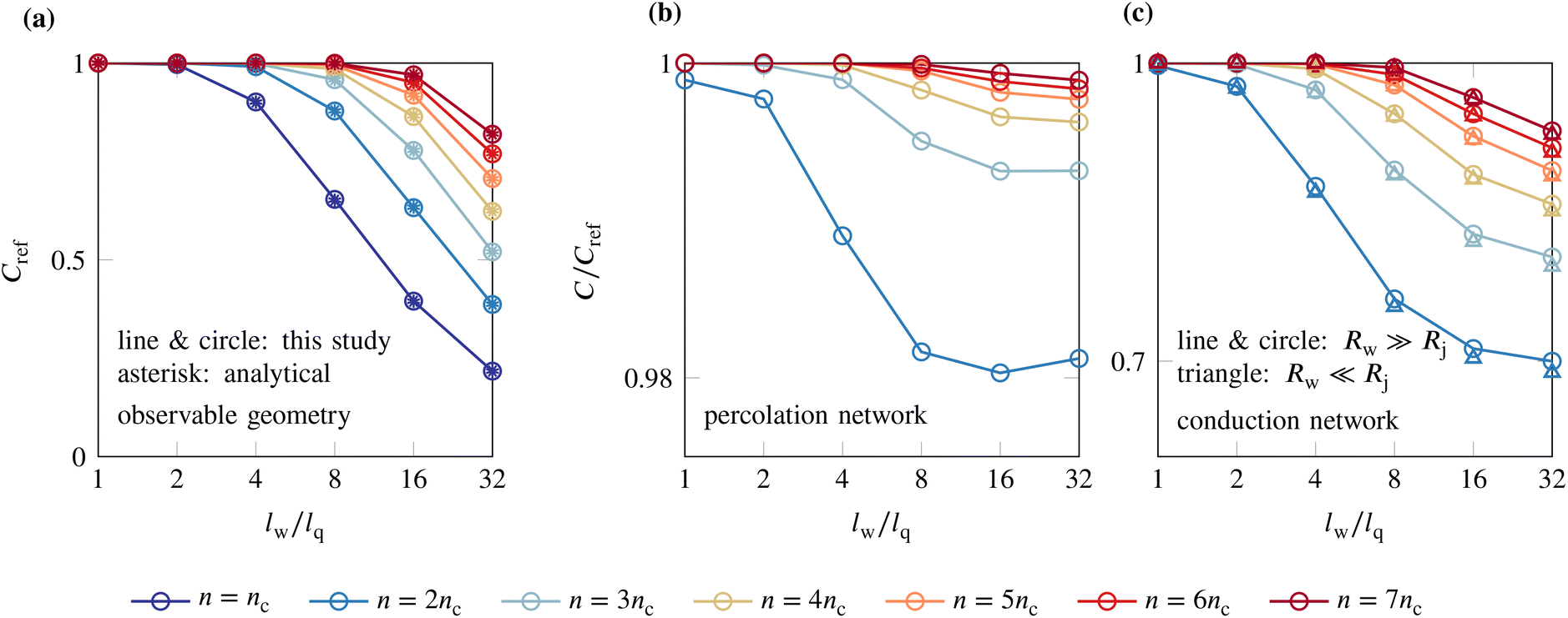 | ||
| Fig. 2 Areal coverage of observable geometry, percolation network and conduction network. (a) Areal coverage (eqn (3)) of observable geometry (Fig. 1d) versus grid resolution lw/lq at different stick density n. The results of the numerical simulations (continuous lines and empty circles) are compared against analytical solution (asterisks). The analytical areal coverage is computed through eqn (S.2) and (S.3) of the ESI.† (b) Areal coverage of the percolation network (Fig. 1e). (c) Areal coverage of the conduction network (Fig. 1f). Results obtained from stick-dominated (Rw ≫ Rj) and junction-dominated (Rw ≪ Rj) resistance are both represented. On the vertical axis of panels (b) and (c) the areal coverage is scaled by the areal coverage of reference Cref at the same stick density n and grid resolution lw/lq (panel (a)). The curves that correspond to n/nc = 6 are actually not shown in panels (b) and (c) for the sake of readability (they are reported in Fig. S4b and c of the ESI†). A log2 scale representation is used for the grid resolution axis. | ||
The areal coverage of percolation and conduction networks is shown in Fig. 2b and c. The areal coverage of the percolation network is computed through eqn (3) by setting Ncriterion as the number of quadrats either containing or intersected by a stick of the percolation network (Fig. 1e). The evaluation of the areal coverage of the conduction network (Fig. 1f) is analogous, but Ncriterion is based on sticks interested by a non-zero current (details are provided in section S1 of the ESI†). The values on the vertical axis in Fig. 2b and c are normalized by Cref at the same stick density n and grid resolution lw/lq (Fig. 2a).
Fig. 2b shows that the areal coverage of the percolation network is already higher than 98% of the areal coverage of the observable geometry when the stick density content n is twice the critical density or larger (i.e., for n ≥ 2nc), confirming that almost all NWs belong to the percolation network when the stick density is ‘well above the critical density’.14,15 Our results are consistent with those by Langley51 who shows that about 99% of the sticks belong to the percolation network at n ≥ 2nc in simulation domains of size L = 4lw (Fig. 3.10b in Langley51).
Fig. 2c shows that the area covered by the conduction network is significantly smaller than the area covered by the observable geometry and the percolation network. For example, the ratio C/Cref at lw/lq = 32 is equal to 0.98 at the least for the percolation network (at n = 2nc, Fig. 2b), while it is equal to 0.93 at the most for the conduction network (with n = 7nc, Fig. 2c). This trend is consistent with the results by Han et al.20 They estimate that a portion equivalent to about 60 to 95% of the observable geometry makes up the conduction network (electrical backbone in their work) when the fiber content ranges between nc and 5nc.
Fig. 1g shows three areal power density maps of the same conduction network at three different resolutions. The inhomogeneous areal power density maps indicate an inhomogeneous workload of the electrode. Workload is null where the areal power density is zero. In these inactive regions the current density is zero because NWs are (i) absent, (ii) disconnected from the percolation network, or (iii) not contributing to the conduction process. Workload is high where the areal power density is high. As the electric current density is significant in these regions, they are relevant to electrode integrity. Joule heating may cause temperature rise resulting in hot-spots initiating local failures in the worst-case scenario. Both null and high workload regions are undesirable when homogeneity is sought.
The distribution of the areal power density on the electrode surface reflects the distribution of the electric current in the electrode. An electrical homogeneity indicator can thus be defined by assessing the areal power density distribution. The spatial assessment of the areal power density is performed by comparing the areal power density  of a single quadrat against the areal power density
  of the entire electrode. We then compute the areal coverage through eqn (3) where Ncriterion is the number of quadrats whose areal power density exceeds a certain percentage of
  . The process is repeated over the entire range of grid resolutions explored. The actual procedure is described next.
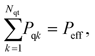
The effective power (the power of the entire electrode) is
| Peff = IeffΔV. | (4) |
Numerical simulations are performed with the value of the potential difference ΔV reported in Table S2 of the ESI.† The resulting effective conductivity (eqn (2)) is reported in Fig. S2b of the ESI.† The power Pq of each quadrat is the power associated to the conduction network in the region identified by the quadrat (refer to section S1.5 of the ESI† for details). The effective areal power density and the areal power density of a single quadrat are defined by
 | (5) |
 | (6) |
irrespective of the number of quadrats Nqt (i.e., irrespective of the grid resolution lw/lq). The response of the network is homogeneous if the areal power density of each quadrat equals the areal power density of the entire electrode,
 | (7) |
The effective power density  is (indirectly) set by design. Once a NW content is selected to attain a certain conductivity κeff (e.g., through relationships visible in Fig. S2b†), the effective power Peff results from eqn (2) and (4) for a given working potential ΔV, and
  results from eqn (5) for a given domain size L. Ratio
  thus quantifies the extent of the deviation of the local response (NW level and below) from the macroscopic response (network/electrode level).
We are ultimately interested in identifying portions of the network that carry a certain amount of power and we want to measure the surface they cover. Fig. 3a–c show the areal coverage (eqn (3)) computed by selecting Ncriterion as the number of quadrats whose areal power density is strictly above a certain threshold, expressed in terms of ratio  (vertical axis). For example, the values at
  refer to the count of quadrats whose areal power density is
  . Each plot in Fig. 3a–c shows the dependence of the areal coverage on the grid resolution lw/lq (horizontal axis). The areal coverage C is normalized by the areal coverage of reference Cref (at the same stick density n and grid resolution lw/lq) reported in Fig. 2a to emphasize that the extent of the surface in which a certain areal power density is attained is always smaller or equal to the area covered by the observable geometry (the latter is directly related to the transparency of the electrode). Columns refer to stick density n = 2nc (left), 4nc (middle), and 6nc (right). Rows refer to resistance scenarios Rw ≫ Rj (a), Rw = Rj (b), and Rw ≪ Rj (c). The resulting map represents the spatial electrical homogeneity.
 | ||
Fig. 3 Areal coverage dependence on grid resolution lw/lq and areal power density threshold  for the numerical geometries. A log2 scale representation is used for the grid resolution axis. (a–c) Contour maps at stick density n = 2nc (left), 4nc (middle), and 6nc (right). Three resistance scenarios are considered: Rw ≫ Rj (a), Rw = Rj (b), and Rw ≪ Rj (c). The areal coverage is normalized by the areal coverage of reference Cref for a given stick density n and grid resolution lw/lq (Fig. 2a). Contour maps obtained by sampling data at lw/lq = 1, 2, 4, 8, 16, and 32, and at for the numerical geometries. A log2 scale representation is used for the grid resolution axis. (a–c) Contour maps at stick density n = 2nc (left), 4nc (middle), and 6nc (right). Three resistance scenarios are considered: Rw ≫ Rj (a), Rw = Rj (b), and Rw ≪ Rj (c). The areal coverage is normalized by the areal coverage of reference Cref for a given stick density n and grid resolution lw/lq (Fig. 2a). Contour maps obtained by sampling data at lw/lq = 1, 2, 4, 8, 16, and 32, and at  between 0 and 3 with spacing 0.1. For each NW content, the areal coverage values are determined as the average of 100 samples. (d) Contour map representing the ideal homogeneous response. (e) Homogeneity index between 0 and 3 with spacing 0.1. For each NW content, the areal coverage values are determined as the average of 100 samples. (d) Contour map representing the ideal homogeneous response. (e) Homogeneity index  versus stick density. Continuous lines and full circles refer to numerical geometries. Isolated symbols refer to the x direction evaluation performed on experimental geometries (Fig. 4a). The same color is used to identify the same resistance scenario. versus stick density. Continuous lines and full circles refer to numerical geometries. Isolated symbols refer to the x direction evaluation performed on experimental geometries (Fig. 4a). The same color is used to identify the same resistance scenario. | ||
The plots show that the responses of the electrode with Rw ≫ Rj (Fig. 3a) and Rw = Rj (Fig. 3b) are similar. When the areal power density threshold  is set, a main trend emerges: the areal coverage depends monotonically on the grid resolution, either directly
 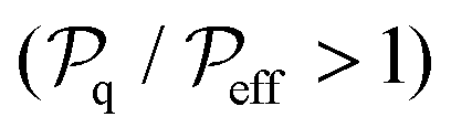 or inversely
  . Exceptions to this trend are modest and limited to either stick density n = 2nc or in the proximity of the region characterised by
  . A slightly different behavior emerges for Rw ≪ Rj (Fig. 3c). For a fixed areal power density threshold above
  , a minimum is attained in the range from lw/lq = 2 to lw/lq = 16 (the actual location depends on the value of
  ). This behavior is appreciable in all the maps in Fig. 3c but is prominent at n = 2nc.
The contour map corresponding to the ideal electrical homogeneity is depicted in Fig. 3d. Since the ideal electrical homogeneity is such that eqn (7) holds irrespective of grid resolution, the areal coverage is
 | (8) |
The contour map representation used in Fig. 3 provides a comprehensive description of the response of an electrode over a wide range of grid resolutions. Although the visual comparison of contour maps is useful, it is not practical for optimization strategy purposes. To address this shortcoming we introduce the homogeneity index  , a scalar indicator that concisely quantifies the difference between the average response of the electrode at a given NW content (represented through contour maps in Fig. 3a–c), and the homogeneous reference response (represented through the contour map in Fig. 3d). This is readily achieved noticing that each contour map in Fig. 3 represents a surface (a single value of C/Cref is determined for each couple of values
  and lw/lq). In particular, Fig. 3d represents a step function (eqn (8)) on a two-dimensional domain. We thus compute
  as a measure of the volume of the region between the step function and the surface describing the response of the electrode of interest. A more detailed description is provided in section S4 of the ESI.†
Fig. 3e reports  for stick density n between nc and 7nc. Continuous curves refer to scenarios Rw ≫ Rj (blue), Rw = Rj (yellow), and Rw ≪ Rj (red). The closer
  is to zero the better the response of the electrode approaches the homogeneous workload. Going from n = nc to n = 7nc, the homogeneity index roughly halves for scenarios Rw ≫ Rj and Rw = Rj, while it reduces by about 30% with Rw ≪ Rj. In our parametric study, the best approximation of the ideal electrical homogeneity corresponds to
  , which is attained at n = 7nc with Rw ≫ Rj. The stick-dominated scenario (Rw ≫ Rj) better approximates the ideal electrical homogeneity at any stick density except for n = nc; it also shows the highest rate of convergence toward electrical homogeneity (
 shows the highest rate of decay). The junction-dominated scenario (Rw ≪ Rj) is affected by a power localization phenomenon at the contact points between sticks. These high power punctual sites hinder power spreading, ultimately slowing down convergence toward an ideal electrical homogeneity. If the resolution of the grid is larger than the characteristic size of the junction, then the assumption of treating junctions as points can be deemed a reasonable approximation. We regard this approximation as adequate if the condition lq > dw is satisfied. In this study, we used the finest grid discretization with a ratio of lw/lq = 32. According to the values of lw and dw specified in Table S2 of the ESI,† the finest grid discretization leads to lq ≈ 1.1 μm and dw = 6.5 × 10⁻² μm. Since lq > dw is always met, the junctions can be treated as point-like entities in this case. The lower rate of decay of
  for Rw ≪ Rj is evident by comparing red and blue lines in Fig. 3e—such an observation could have also been drawn by comparing Fig. 3c and a (as n increases from 2nc to 6nc). Our conclusions are based on the quantitative evaluation of electrical homogeneity that takes into account all locations of the geometry under evaluation and considers multiple length scales at the same time. Our analysis strengthen the qualitative observations by Žeželj and Stanković14 who predict the distribution of electric current to even out as the ratio Rw/Rj increases.
The equally contributing resistance scenario (Rw = Rj, yellow curve) approximates the stick-dominated scenario (Rw ≫ Rj, blue curve) over the entire range of stick density. The blue and yellow curves exhibit significant overlap until n = 3nc, with a maximum relative difference of only 15% between the corresponding values of  . In contrast, the relative difference between the junction-dominated and equally contributing response can be as high as 58%. Controlling the sheet resistance and improving the stability of metal NW electrodes requires mitigating the effect of junction resistance. To achieve this, various strategies have been proposed to enhance the welding of junctions. These strategies include thermal annealing,6 localized joule heating,52 mechanical pressing,33 capillarity-driven welding,53 alcohol-based chemical welding,54 laser nano-welding,35,40,55 plasmonic welding,34 and using hierarchical multiscale hybrid nanocomposites.56 Although having a negligible junction resistance (condition Rw/Rj ≫ 1) is ideal, many of the proposed strategies for enhancing the welding of junctions result in conditions where Rw/Rj falls in the range between approximately 1 and much greater than 1.34,35,52,53 However, based on the results in Fig. 3, it can be inferred that reducing the junction resistance excessively (with the aim of achieving Rw/Rj > 1) may not always be a worthwhile strategy, since it is likely to result in only a marginal improvement in electrical homogeneity. Therefore, it is recommended to perform a cost-benefit analysis on a case-by-case basis, while taking into account all the design requirements (such as sheet resistance) as well.
2.3. Areal coverage: Experimental samples
Next, spray-coated AgNW depositions are analyzed. We refer to the SEM images by Sannicolo et al.4 The SEM images, reported in Fig. 4a, cover an area of approximately 25 μm × 21.5 μm and show the local morphology of as-fabricated specimens at NW content 50 ± 4 mg m−2 (A1), 63 ± 7 mg m−2 (A2), and 86 ± 7 mg m−2 (A3).4 Sannicolo et al.4 determined the NW content from specimens measuring 25 mm × 25 mm. The SEM images reported in Fig. 4a represents small portions of each of those specimens. The areal coverage is expressed in terms of areal mass density (refer to eqn (S.8) of the ESI†). Nanowires have average length 7 ± 3 μm and average diameter 79 ± 10 nm. | ||
Fig. 4 Areal coverage dependence on grid resolution lavg/lq and areal power density threshold  for the experimental geometries. Results about conduction network in the x-direction. A log2 scale representation is used for the grid resolution axis. (a) SEM images of silver NWs (samples A1, A2 and A3) showing the local morphologies of electrodes analyzed by Sannicolo et al.4 (reprinted with permission from Sannicolo et al.;4 copyright © 2018 American Chemical Society). (b–d) Contour maps generated from the digitization of sample A1 (left), A2 (middle), and A3 (right) as shown in Fig. S3b of the ESI.† Three resistance scenarios are considered: Rw ≫ Rj (a), Rw = Rj (b), and Rw ≪ Rj (c). The areal coverage is normalized by the areal coverage of reference Cref for a given stick density n and grid resolution lavg/lq (Fig. S4a†). Contour maps obtained by sampling data at lavg/lq = 1, 2, 4, 8, 16, and 32, and at for the experimental geometries. Results about conduction network in the x-direction. A log2 scale representation is used for the grid resolution axis. (a) SEM images of silver NWs (samples A1, A2 and A3) showing the local morphologies of electrodes analyzed by Sannicolo et al.4 (reprinted with permission from Sannicolo et al.;4 copyright © 2018 American Chemical Society). (b–d) Contour maps generated from the digitization of sample A1 (left), A2 (middle), and A3 (right) as shown in Fig. S3b of the ESI.† Three resistance scenarios are considered: Rw ≫ Rj (a), Rw = Rj (b), and Rw ≪ Rj (c). The areal coverage is normalized by the areal coverage of reference Cref for a given stick density n and grid resolution lavg/lq (Fig. S4a†). Contour maps obtained by sampling data at lavg/lq = 1, 2, 4, 8, 16, and 32, and at  between 0 and 3 with spacing 0.2. between 0 and 3 with spacing 0.2. | ||
We perform the spatial assessment following the procedure summarized in Fig. 1. The digital replicas of the geometries are created by first assuming that the NWs can be approximated as straight sticks (Fig. S3a of the ESI†). A similar approach is pursued, e.g., in Gomes da Rocha et al.9 and Kim and Nam.8 Squared subsets of the resulting geometries are extracted next (Fig. S3b of the ESI†). The identification of percolation and conduction networks is performed considering the squared subsets shown in Fig. S3b.† The digitization procedure and the characterization of each geometry are described in section S5.1 of the ESI.†
The size of the squared subsets (Fig. S3b†) is L ≈ 4lavg, being lavg ≈ 4.7 μm the average length of the sticks (Fig. S3c†) and L ≈ 21.5 μm. In section S5.1 of the ESI† we demonstrate that the NWs contained in the squared subsets correspond to n = 6, 12, and 18, and that the grid resolution ranges between 1 and 32 (to a good degree of approximation) if expressed in terms of lavg/lq. The comparison against the results presented in the previous sections is thus appropriate. The values of the contour maps in Fig. 4 are scaled by the values of Cref computed from the observable geometries A1, A2, and A3 (one at a time), which are reported in Fig. S4a of the ESI.† The applicability of the computational strategy to experimental samples is not restricted to n ≤ 18. As the objective of this investigation is to validate the computational strategy through comparison with experimental results, a thorough characterization of the experimental samples is required. Sannicolo et al.4 provide a comprehensive analysis of electrode properties such as areal mass density, sheet resistance, and electrical homogeneity, as well as NW properties including average diameter and length. However, their study is limited to samples A1, A2, and A3 in terms of NW content.
The spatial assessment of the electrical response is performed for scenarios Rw ≫ Rj, Rw = Rj, and Rw ≪ Rj. The results about the conduction network in the x-direction are shown in Fig. 4b–d. Since the NWs arrangements of the SEM images lead to macroscopic responses that differ for x- and y-directions, (section S5.1 of the ESI†), Fig. S5† presents the results of the spatial analyses for the conduction network in the y-direction. The contour plots in Fig. 4 are less smooth than those in Fig. 3 because the former refer to one sample for each NW content while the latter are the average of 100 realizations for each stick density n. The main trends are nevertheless consistent with those deducible from Fig. 3: the ideal electrical homogeneity is better approached as (i) the stick-dominated condition is approached (from Fig. 4d to b), and (ii) the NW content increases (from sample A1 to A3). The NW content-homogeneity relationship identified in this work is consistent with experimental observations by Sannicolo et al.4 who comment that ‘the network density influences not only the overall conduction level of the network (resistance value) but also the local electrical distribution […]’. They ultimately conclude that ‘dense networks afford higher electrical homogeneity’.
Shifting from sample A1 to A2 with Rw ≫ Rj and Rw = Rj (Fig. 4b and c) the direct relationship between NW content and homogeneity seems to fail. We attribute the reason to the following aspects. First, the NWs in sample A1 are preferentially aligned along the x-direction (refer to Fig. S3d of the ESI†) thus causing an anisotropic response of the electrode (notice the different sheet conductivity values in x- and y-directions reported in Tables S3 and S4 of the ESI†). Second, the NWs in the SEM images have different lengths and a few longer NWs drive the conduction of sample A1 in the x-direction (refer to Fig. 4a and S3b†). Once again, our observations agree with the experimental observations by Sannicolo et al.4 who conclude that deposition methods entailing preferential NWs orientations should be considered with caution if high level of electrical homogeneity are desirable. Notice that the spatial assessment of the conduction network in the y-direction fulfills the expectation (refer to results for samples A1 and A2 in Fig. S5a and b†).
To facilitate a direct comparison between distributions generated numerically and those obtained experimentally with similar NW content, the results of the spatial assessment of numerically generated geometries at n = nc, 2nc, and 3nc are reported in Fig. S6.† Differences are appreciable between numerically generated geometries at n = nc (n = 6) and sample A1. We attribute the reason to the fact that (i) as the percolation threshold is approached, small fluctuations of NW content cause sensibly different responses,10 and (ii) NWs in sample A1 are nonuniformly oriented and with different lengths. We consider the match between numerically generated samples at n = 2nc and 3nc and samples A2 and A3 extremely satisfactory.
To conclude, we report a comparison of our strategy and the network homogeneity assessment performed by Sannicolo et al.4 The investigation conducted in this study can be seen as the microscopic counterpart of the work by Sannicolo et al.,4 which focused on the macroscopic level. Sannicolo et al.4 reconstruct the voltage map of 25 mm × 25 mm specimens through one-probe electrical mapping with scanning step of 1.0 mm. Their sampling map is more than two orders of magnitude coarser than our grid resolution: using the notation adopted in this work, the sampling by Sannicolo et al.4 is in the range lavg/lq ≈ 0.007 (with an average NW length lavg = 7 μm), while our investigation is performed at lavg/lq ≥ 1. A few other differences should be kept in mind while performing the comparison. First, Sannicolo et al.4 do not explicitly provide information about the percolation threshold. We therefore deduce nc by analogy with our own investigation. Second, Sannicolo et al.4 do not conduct a specific investigation to determine the junction resistance values or provide an average value of the ratio Rw/Rj in their characterization of the AgNW networks. This lack of knowledge supports the adoption of the simplest modeling assumption, which considers equal Rj values for all junctions. This modeling assumption represents the minimum parameter set required to simulate a wide range of electrode responses, from those dominated by sticks (Rw ≫ Rj) to those dominated by junctions (Rw ≪ Rj). The results obtained with equal Rj for all junction provide the upper and lower bounds for the electrode response in terms of electrical homogeneity. In fact, it is reasonable to expect that non-uniform distributions of junction resistance values result in electrical homogeneity comparable to those presented in this study if stick-dominated, equally contributing, and junction-dominated resistance scenarios are approached in an average sense. Third, our numerical simulations are performed by assuming AgNWs as straight sticks although they are slightly bent in the SEM images by Sannicolo et al.4 shown in Fig. 4a. Fourth, the observable geometries of our numerical samples are periodic (Fig. 1a), while those from the SEM images (Fig. 4a) are not. Fifth, the SEM images show portions of the specimens studied by Sannicolo et al.4 which are not strictly representative of the specimens they have been extracted from. A thorough discussion about this aspect is given in section S5.1 of the ESI.† Nevertheless, we stress that the computational strategy proposed in this work is applicable irrespective of the size of the portion of surface to be analyzed. There are no limitations on the size of the region provided that images of the morphology with a sufficiently high resolution are available, that is, as long as the NWs can be distinguished. Because of these arguments, an exact match between the conclusions of the two assessment criteria cannot be realistically expected. These aspects need to be carefully considered if the computational strategy presented in this work is integrated with experimental analyses for NWs electrodes optimization purposes. The definition of such a strategy however falls beyond the scope of the current contribution.
Sannicolo et al.4 quantify the degree of (in)homogeneity of the electrical response through the electrical tortuosity, defined as the tortuosity of the voltage equipotential lines. They identify an inverse correlation between the electrical tortuosity and the network homogeneity (values are reported in Table S5 of the ESI†). The authors conclude that the network with the lowest density (associated to sample A1 in Fig. 4a) has an electrical tortuosity roughly 30% higher than the two other specimens (associated to samples A2 and A3 in the same figure) and is thus less homogeneous. Fig. 3e shows  corresponding to the contour maps in Fig. 4 (x-direction). The values computed for samples A1, A2, and A3 have been inserted at n = nc, n = 2nc, and n = 3nc respectively, in view of the arguments exposed above. We observe that the overall trend is consistent with the trend found with the numerically generated geometries, and, not surprisingly, discrepancies are the largest for sample A1. From the analysis of the numerically generated geometries (continuous lines in Fig. 3e) we find that
  changes by about 50% (Rw ≫ Rj, blue line) and 19% (Rw ≪ Rj, red line) from n = nc to n = 3nc, respectively. From the analysis of the experimentally obtained geometries (symbols in Fig. 3e) we find that
  changes by about 35% (Rw ≫ Rj, blue empty symbols) and 10% (Rw ≪ Rj, red empty symbols) in the x-direction from sample A1 to sample A3, respectively. The full set of data is available in Table S5 of the ESI,† and it includes the evaluations performed along the y-direction. The electrical tortuosity and the homogeneity index are not exactly equivalent. The former assumes values ≥1, with the homogeneous response corresponding to an electrical tortuosity equal to 1, while the latter assumes values ≥0, with the homogeneous response corresponding to
  . Nevertheless, the relative changes from specimens A1 to A3 fall within the same range of values (32% according to Sannicolo et al.,4 and between 8% and 38% according to our evaluation), suggesting that the two homogeneity assessments are consistent. The comparison thus provides a rough validation of our strategy, demonstrating its applicability to experimentally obtained geometries too. We stress that a comprehensive homogeneity assessment can be achieved by complementing experimental procedures with the framework proposed in this contribution. The framework allows to explore length scales hardly accessible experimentally (in the order of NWs length and below) in a rather straightforward manner.
3. Conclusions
We propose a computational strategy for electrical homogeneity assessment of NW electrodes. We show that electrical homogeneity evaluations based on macroscopic observations are not exhaustive as the area covered by the observable geometry exceeds the area covered by the conducting network. Condition C/Cref ≤ 1 is met under all explored circumstances, and the actual value of C/Cref strongly depends on the length scale of observation (lw/lq).As a uniform network utilization is mandatory for NW electrode stability, electrode design procedures should intrinsically entail electrical homogeneity considerations. The analysis of the areal power density and the ensuing homogeneity index  support this task. The resulting homogeneity index
  is a scalar indicator, not bounded to a single length scale, that provides a quantitative and objective evaluation of electrical homogeneity (it does not entail qualitative visual inspections of the electric current distribution, for example). The homogeneity index is suitable for NW electrode design optimization. For example, it can be employed to integrate NWs content optimization procedures, usually restricted to the transmittance-sheet resistance trade-off,18,20,24,25,36,39,40,43,44,56 with an electrical homogeneity descriptor.
This investigation demonstrates that the nanowire-to-junction resistance ratio Rw/Rj is crucial for the NW content-electrical homogeneity relationship. Based on the results reported in Fig. 3e we conclude that the reduction of the junction resistance below the NW resistance should be pursued only if necessary (e.g., for the sake of effective conductivity enhancement), as it results in modest benefits in terms of electrical homogeneity (compare Rw ≫ Rj and Rw = Rj curves in Fig. 3e).
The proposed strategy has the potential to complement experimental investigations, providing a useful tool to evaluate the homogeneity of the power density distribution in the electrode. The power density assessment strategy shown in Fig. 1g is versatile and can be applied also to thermal maps, which indirectly represent the electrical power density distribution in the electrode.1,5,10,11,23,29,46
Moreover, by utilizing image digitization software,57,58 it is possible to attain digital replicas of electrode microstructure images and standardize the procedure outlined in section 2.3. This step is particularly useful because if images of the electrode morphology are available (such as those reported in Fig. 4a), the procedure can access length scales that are experimentally impractical (in the order of NW length and further below).
To optimize the significance of the homogeneity evaluation and expedite experimental inquiries, the range of grid resolutions can be adjusted to match the characteristic length scales of a particular NW electrode application. This flexibility further enhances the value of the proposed strategy, making it suitable for a wide range of applications such as battery electrodes,59,60 conductive/piezoelectric membranes,61–63 air filters with active sterilization,37 and fuel cells.64 In all these applications, the conduction process of a network of one-dimensional components, such as nanowires, nanotubes, and nanofibers, ultimately determines the overall system response.
Author contributions
D. Grazioli: conceptualization, data curation, formal analysis, investigation, methodology, project administration, software, supervision, validation, visualization, writing – original draft, writing – review and editing. A.C. Dadduzio: formal analysis, investigation, software, writing – review and editing. M. Roso: writing – review and editing. A. Simone: funding acquisition, resources, supervision, writing – review and editing.Conflicts of interest
There are no conflicts to declare.References
- T. Sannicolo, M. Lagrange, A. Cabos, C. Celle, J.-P. Simonato and D. Bellet, Metallic nanowire-based transparent electrodes for next generation flexible devices: A review, Small, 2016, 12(44), 6052–6075, DOI:10.1002/smll.201602581.
- D. T. Papanastasiou, A. Schultheiss, D. Muñoz-Rojas, C. Celle, A. Carella, J.-P. Simonato and D. Bellet, Transparent heaters: A review, Adv. Funct. Mater., 2020, 30(21), 1910225, DOI:10.1002/adfm.201910225.
- J. J. Patil, W. H. Chae, A. Trebach, K.-J. Carter, E. Lee, T. Sannicolo and J. C. Grossman, Failing forward: Stability of transparent electrodes based on metal nanowire networks, Adv. Mater., 2020, 33(5), 2004356, DOI:10.1002/adma.202004356.
- T. Sannicolo, N. Charvin, L. Flandin, S. Kraus, D. T. Papanastasiou, C. Celle, J.-P. Simonato, D. Muñoz-Rojas, C. Jiménez and D. Bellet, Electrical mapping of silver nanowire networks: A versatile tool for imaging network homogeneity and degradation dynamics during failure, ACS Nano, 2018, 12(5), 4648–4659, DOI:10.1021/acsnano.8b01242.
- H. H. Khaligh, L. Xu, A. Khosropour, A. Madeira, M. Romano, C. Pradére, M. Tréguer-Delapierre, L. Servant, M. A. Pope and I. A. Goldthorpe, The Joule heating problem in silver nanowire transparent electrodes, Nanotechnology, 2017, 28(42), 425703, DOI:10.1088/1361-6528/aa7f34.
- D. P. Langley, M. Lagrange, G. Giusti, C. Jiménez, Y. Bréchet, N. D. Nguyen and D. Bellet, Metallic nanowire networks: Effects of thermal annealing on electrical resistance, Nanoscale, 2014, 6(22), 13535–13543, 10.1039/c4nr04151h.
- D. Kim and J. Nam, Systematic analysis for electrical conductivity of network of conducting rods by Kirchhoff's laws and block matrices, J. Appl. Phys., 2018, 124(21), 215104, DOI:10.1063/1.5051390.
- D. Kim and J. Nam, Electrical conductivity analysis for networks of conducting rods using a block matrix approach: A case study under junction resistance dominant assumption, J. Phys. Chem. C, 2019, 124(1), 986–996, DOI:10.1021/acs.jpcc.9b07163.
- C. G. da Rocha, H. G. Manning, C. O'Callaghan, C. Ritter, A. T. Bellew, J. J. Boland and M. S. Ferreira, Ultimate conductivity performance in metallic nanowire networks, Nanoscale, 2015, 7(30), 13011–13016, 10.1039/c5nr03905c.
- T. Sannicolo, D. Muñoz-Rojas, N. D. Nguyen, S. Moreau, C. Celle, J.-P. Simonato, Y. Bréchet and D. Bellet, Direct imaging of the onset of electrical conduction in silver nanowire networks by infrared thermography: Evidence of geometrical quantized percolation, Nano Lett., 2016, 16(11), 7046–7053, DOI:10.1021/acs.nanolett.6b03270.
- K. Maize, S. R. Das, S. Sadeque, A. M. S. Mohammed, A. Shakouri, D. B. Janes and M. A. Alam, Super-Joule heating in graphene and silver nanowire network, Appl. Phys. Lett., 2015, 106(14), 143104, DOI:10.1063/1.4916943.
- A. Kumar and G. U. Kulkarni, Evaluating conducting network based transparent electrodes from geometrical considerations, J. Appl. Phys., 2016, 119(1), 015102, DOI:10.1063/1.4939280.
- C. Forró, L. Demkó, S. Weydert, J. Vörös and K. Tybrandt, Predictive model for the electrical transport within nanowire networks, ACS Nano, 2018, 12(11), 11080–11087, DOI:10.1021/acsnano.8b05406.
- M. Žeželj and I. Stanković, From percolating to dense random stick networks: Conductivity model investigation, Phys. Rev. B, 2012, 86(13), 134202, DOI:10.1103/physrevb.86.134202.
- A. Kumar, N. S. Vidhyadhiraja and G. U. Kulkarni, Current distribution in conducting nanowire networks, J. Appl. Phys., 2017, 122(4), 045101, DOI:10.1063/1.4985792.
- Y. Y. Tarasevich, I. V. Vodolazskaya, A. V. Eserkepov and R. K. Akhunzhanov, Electrical conductance of two-dimensional composites with embedded rodlike fillers: An analytical consideration and comparison of two computational approaches, J. Appl. Phys., 2019, 125(13), 134902, DOI:10.1063/1.5092351.
- J. Li and S.-L. Zhang, Finite-size scaling in stick percolation, Phys. Rev. E, 2009, 80(4), 040104, DOI:10.1103/physreve.80.040104.
- R. M. Mutiso, M. C. Sherrott, A. R. Rathmell, B. J. Wiley and K. I. Winey, Integrating simulations and experiments to predict sheet resistance and optical transmittance in nanowire films for transparent conductors, ACS Nano, 2013, 7(9), 7654–7663, DOI:10.1021/nn403324t.
- M. Jagota and N. Tansu, Conductivity of nanowire arrays under random and ordered orientation configurations, Sci. Rep., 2015, 5(1), 10219, DOI:10.1038/srep10219.
- F. Han, T. Maloth, G. Lubineau, R. Yaldiz and A. Tevtia, Computational investigation of the morphology, efficiency, and properties of silver nano wires networks in transparent conductive film, Sci. Rep., 2018, 8(1), 17494, DOI:10.1038/s41598-018-35456-7.
- Y. Y. Tarasevich, A. S. Burmistrov, V. A. Goltseva, I. I. Gordeev, V. I. Serbin, A. A. Sizova, I. V. Vodolazskaya and D. A. Zholobov, Identification of current-carrying part of a random resistor network: Electrical approaches vs. graph theory algorithms, J. Phys.: Conf. Ser., 2018, 955, 012021, DOI:10.1088/1742-6596/955/1/012021.
- N. Fata, S. Mishra, Y. Xue, Y. Wang, J. Hicks and A. Ural, Effect of junction-to-nanowire resistance ratio on the percolation conductivity and critical exponents of nanowire networks, J. Appl. Phys., 2020, 128(12), 124301, DOI:10.1063/5.0023209.
- N. Charvin, J. Resende, D. T. Papanastasiou, D. Muñoz-Rojas, C. Jiménez, A. Nourdine, D. Bellet and L. Flandin, Dynamic degradation of metallic nanowire networks under electrical stress: A comparison between experiments and simulations, Nanoscale Adv., 2021, 3(3), 675–681, 10.1039/d0na00895h.
- E. M. Doherty, S. De, P. E. Lyons, A. Shmeliov, P. N. Nirmalraj, V. Scardaci, J. Joimel, W. J. Blau, J. J. Boland and J. N. Coleman, The spatial uniformity and electromechanical stability of transparent, conductive films of single walled nanotubes, Carbon, 2009, 47(10), 2466–2473, DOI:10.1016/j.carbon.2009.04.040.
- S. De, T. M. Higgins, P. E. Lyons, E. M. Doherty, P. N. Nirmalraj, W. J. Blau, J. J. Boland and J. N. Coleman, Silver nanowire networks as flexible, transparent, conducting films: Extremely high DC to optical conductivity ratios, ACS Nano, 2009, 3(7), 1767–1774, DOI:10.1021/nn900348c.
- S. Cho, S. Kang, A. Pandya, R. Shanker, Z. Khan, Y. Lee, J. Park, S. L. Craig and H. Ko, Large-area cross-aligned silver nanowire electrodes for flexible, transparent, and force-sensitive mechanochromic touch screens, ACS Nano, 2017, 11(4), 4346–4357, DOI:10.1021/acsnano.7b01714.
- R. Gupta and G. U. Kulkarni, Holistic method for evaluating large area transparent conducting electrodes, ACS Appl. Mater. Interfaces, 2013, 5(3), 730–736, DOI:10.1021/am302264a.
- B. W. An, B. G. Hyun, S.-Y. Kim, M. Kim, M.-S. Lee, K. Lee, J. B. Koo, H. Y. Chu, B.-S. Bae and J.-U. Park, Stretchable and transparent electrodes using hybrid structures of graphene–metal nanotrough networks with high performances and ultimate uniformity, Nano Lett., 2014, 14(11), 6322–6328, DOI:10.1021/nl502755y.
- Y. Fang, K. Ding, Z. Wu, H. Chen, W. Li, S. Zhao, Y. Zhang, L. Wang, J. Zhou and B. Hu, Architectural engineering of nanowire network fine pattern for 30 μm wide flexible quantum dot light-emitting diode application, ACS Nano, 2016, 10(11), 10023–10030, DOI:10.1021/acsnano.6b04506.
- K. M. Kam, L. Zeng, Q. Zhou, R. Tran and J. Yang, On assessing spatial uniformity of particle distributions in quality control of manufacturing processes, J. Manuf. Syst., 2013, 32(1), 154–166, DOI:10.1016/j.jmsy.2012.07.018.
- C. Darcel, O. Bour, P. Davy and J. R. de Dreuzy, Connectivity properties of two-dimensional fracture networks with stochastic fractal correlation, Water Resour. Res., 2003, 39(10), 1272, DOI:10.1029/2002wr001628.
- R. P. Taylor, B. Spehar, P. V. Donkelaar and C. M. Hagerhall, Perceptual and physiological responses to Jackson Pollock’s fractals, Front. Hum. Neurosci., 2011, 5, 1, DOI:10.3389/fnhum.2011.00060.
- T. Tokuno, M. Nogi, M. Karakawa, J. Jiu, T. T. Nge, Y. Aso and K. Suganuma, Fabrication of silver nanowire transparent electrodes at room temperature, Nano Res., 2011, 4(12), 1215–1222, DOI:10.1007/s12274-011-0172-3.
- E. C. Garnett, W. Cai, J. J. Cha, F. Mahmood, S. T. Connor, M. G. Christoforo, Y. Cui, M. D. McGehee and M. L. Brongersma, Self-limited plasmonic welding of silver nanowire junctions, Nat. Mater., 2012, 11(3), 241–249, DOI:10.1038/nmat3238.
- Q. Nian, M. Saei, Y. Xu, G. Sabyasachi, B. Deng, Y. P. Chen and G. J. Cheng, Crystalline nanojoining silver nanowire percolated networks on flexible substrate, ACS Nano, 2015, 9(10), 10018–10031, DOI:10.1021/acsnano.5b03601.
- J. Lee, K. An, P. Won, Y. Ka, H. Hwang, H. Moon, Y. Kwon, S. Hong, C. Kim, C. Lee and S. H. Ko, A dual-scale metal nanowire network transparent conductor for highly efficient and flexible organic light emitting diodes, Nanoscale, 2017, 9(5), 1978–1985, 10.1039/c6nr09902e.
- S. Han, J. Kim, Y. Lee, J. Bang, C. G. Kim, J. Choi, J. Min, I. Ha, Y. Yoon, C.-H. Yun, M. Cruz, B. J. Wiley and S. H. Ko, Transparent air filters with active thermal sterilization, Nano Lett., 2022, 22(1), 524–532, DOI:10.1021/acs.nanolett.1c02737.
- J. H. Lee, P. Lee, D. Lee, S. S. Lee and S. H. Ko, Large-scale synthesis and characterization of very long silver nanowires via successive multistep growth, Cryst. Growth Des., 2012, 12(11), 5598–5605, DOI:10.1021/cg301119d.
- B. Bari, J. Lee, T. Jang, P. Won, S. H. Ko, K. Alamgir, M. Arshad and L. J. Guo, Simple hydrothermal synthesis of very-long and thin silver nanowires and their application in high quality transparent electrodes, J. Mater. Chem. A, 2016, 4(29), 11365–11371, 10.1039/c6ta03308c.
- J. Lee, P. Lee, H. Lee, D. Lee, S. S. Lee and S. H. Ko, Very long Ag nanowire synthesis and its application in a highly transparent, conductive and flexible metal electrode touch panel, Nanoscale, 2012, 4(20), 6408, 10.1039/c2nr31254a.
- M. Bobinger, J. Mock, P. L. Torraca, M. Becherer, P. Lugli and L. Larcher, Tailoring the aqueous synthesis and deposition of copper nanowires for transparent electrodes and heaters, Adv. Mater. Interfaces, 2017, 4(20), 1700568, DOI:10.1002/admi.201700568.
- S. Han, S. Hong, J. Yeo, D. Kim, B. Kang, M.-Y. Yang and S. H. Ko, Nanorecycling: Monolithic integration of copper and copper oxide nanowire network electrode through selective reversible photothermochemical reduction, Adv. Mater., 2015, 27(41), 6397–6403, DOI:10.1002/adma.201503244.
- C. Celle, A. Cabos, T. Fontecave, B. Laguitton, A. Benayad, L. Guettaz, N. Pélissier, V. H. Nguyen, D. Bellet, D. Muñoz-Rojas and J.-P. Simonato, Oxidation of copper nanowire based transparent electrodes in ambient conditions and their stabilization by encapsulation: Application to transparent film heaters, Nanotechnology, 2018, 29(8), 085701, DOI:10.1088/1361-6528/aaa48e.
- M. Lagrange, D. P. Langley, G. Giusti, C. Jiménez, Y. Bréchet and D. Bellet, Optimization of silver nanowire-based transparent electrodes: Effects of density, size and thermal annealing, Nanoscale, 2015, 7(41), 17410–17423, 10.1039/c5nr04084a.
- S. Torquato, Random Heterogeneous Materials, Springer New York, 2002. DOI:10.1007/978-1-4757-6355-3.
- D. Estrada and E. Pop, Imaging dissipation and hot spots in carbon nanotube network transistors, Appl. Phys. Lett., 2011, 98(7), 073102, DOI:10.1063/1.3549297.
- G. Hodes and P. V. Kamat, Understanding the implication of carrier diffusion length in photovoltaic cells, J. Phys. Chem. Lett., 2015, 6(20), 4090–4092, DOI:10.1021/acs.jpclett.5b02052.
- A. Kumar, Predicting efficiency of solar cells based on transparent conducting electrodes, J. Appl. Phys., 2017, 121(1), 014502, DOI:10.1063/1.4973117.
- D. Langley, G. Giusti, M. Lagrange, R. Collins, C. Jiménez, Y. Bréchet and D. Bellet, Silver nanowire networks: Physical properties and potential integration in solar cells, Sol. Energy Mater. Sol. Cells, 2014, 125, 318–324, DOI:10.1016/j.solmat.2013.09.015.
- A. Kim, Y. Won, K. Woo, S. Jeong and J. Moon, All-solution-processed indium-free transparent composite electrodes based on Ag nanowire and metal oxide for thin-film solar cells, Adv. Funct. Mater., 2014, 24(17), 2462–2471, DOI:10.1002/adfm.201303518.
- D. Langley, Silver nanowire networks: Effects of percolation and thermal annealing on physical properties, Ph.D. thesis, Université de Grenoble, 2014 Search PubMed.
- T.-B. Song, Y. Chen, C.-H. Chung, Y. M. Yang, B. Bob, H.-S. Duan, G. Li, K.-N. Tu, Y. Huang and Y. Yang, Nanoscale Joule heating and electromigration enhanced ripening of silver nanowire contacts, ACS Nano, 2014, 8(3), 2804–2811, DOI:10.1021/nn4065567.
- T. A. Celano, D. J. Hill, X. Zhang, C. W. Pinion, J. D. Christesen, C. J. Flynn, J. R. McBride and J. F. Cahoon, Capillarity-driven welding of semiconductor nanowires for crystalline and electrically Ohmic junctions, Nano Lett., 2016, 16(8), 5241–5246, DOI:10.1021/acs.nanolett.6b02361.
- H. Lu, D. Zhang, J. Cheng, J. Liu, J. Mao and W. C. H. Choy, Locally welded silver nano-network transparent electrodes with high operational stability by a simple alcohol-based chemical approach, Adv. Funct. Mater., 2015, 25(27), 4211–4218, DOI:10.1002/adfm.201501004.
- S. Hong, H. Lee, J. Yeo and S. H. Ko, Digital selective laser methods for nanomaterials: From synthesis to processing, Nano Today, 2016, 11(5), 547–564, DOI:10.1016/j.nantod.2016.08.007.
- P. Lee, J. Ham, J. Lee, S. Hong, S. Han, Y. D. Suh, S. E. Lee, J. Yeo, S. S. Lee, D. Lee and S. H. Ko, Highly stretchable or transparent conductor fabrication by a hierarchical multiscale hybrid nanocomposite, Adv. Funct. Mater., 2014, 24(36), 5671–5678, DOI:10.1002/adfm.201400972.
- R. Shkarin, A. Shkarin, S. Shkarina, A. Cecilia, R. A. Surmenev, M. A. Surmeneva, V. Weinhardt, T. Baumbach and R. Mikut, Quanfima: An open source python package for automated fiber analysis of biomaterials, PLoS One, 2019, 14(4), e0215137, DOI:10.1371/journal.pone.0215137.
- H. Bai and S. Wu, Deep-learning-based nanowire detection in AFM images for automated nanomanipulation, Nanotechnol. Precis. Eng., 2021, 4(1), 013002, DOI:10.1063/10.0003218.
- J.-W. Jung, C.-L. Lee, S. Yu and I.-D. Kim, Electrospun nanofibers as a platform for advanced secondary batteries: A comprehensive review, J. Mater. Chem. A, 2016, 4(3), 703–750, 10.1039/c5ta06844d.
- M. Zhuo, D. Grazioli and A. Simone, Active material utilization and capacity of fiber-based battery electrodes, Electrochim. Acta, 2020, 333, 134929, DOI:10.1016/j.electacta.2019.134929.
- M. Roso, A. Lorenzetti, C. Boaretti and M. Modesti, Electrically conductive membranes obtained by simultaneous electrospinning and electrospraying processes, J. Nanomater., 2016, 2016, 1–11, DOI:10.1155/2016/8362535.
- Y. Jeon, Y. Ji, Y. I. Cho, C. Lee, D.-H. Park and Y.-G. Shul, Oxide–carbon nanofibrous composite support for a highly active and stable polymer electrolyte membrane fuel-cell catalyst, ACS Nano, 2018, 12(7), 6819–6829, DOI:10.1021/acsnano.8b02040.
- D. Huang, X. Li, C. Luo, P. Wei, Y. Sui, J. Wen, C. Cong, X. Zhang, X. Meng and Q. Zhou, Consecutive and reliable proton transfer channels construction based on the compatible interface between nanofiber and SPEEK, J. Membr. Sci., 2022, 662, 121001, DOI:10.1016/j.memsci.2022.121001.
- K. Lee, J. Zhang, H. Wang and D. P. Wilkinson, Progress in the synthesis of carbon nanotube- and nanofiber-supported pt electrocatalysts for PEM fuel cell catalysis, J. Appl. Electrochem., 2006, 36(5), 507–522, DOI:10.1007/s10800-006-9120-4.
Footnote |
| † Electronic supplementary information (ESI) available. See DOI: https://doi.org/10.1039/d2nr06564a |
| This journal is © The Royal Society of Chemistry 2023 |