
 Open Access Article
 This Open Access Article is licensed under a Creative Commons Attribution-Non Commercial 3.0 Unported Licence
Site-selective functionalization of in-plane nanoelectrode-antennas†
Maximilian
Ochs‡
 a,
Laurent
Jucker‡
b,
Maximilian
Rödel
c,
Monika
Emmerling
a,
René
Kullock
a,
Jens
Pflaum
c,
Marcel
Mayor
*bde and
Bert
Hecht
*a
a,
Laurent
Jucker‡
b,
Maximilian
Rödel
c,
Monika
Emmerling
a,
René
Kullock
a,
Jens
Pflaum
c,
Marcel
Mayor
*bde and
Bert
Hecht
*a
aNanoOptics & Biophotonics Group, Experimental Physics 5, University of Würzburg, Am Hubland, 97074 Würzburg, Germany. E-mail: hecht@physik.uni-wuerzburg.de
bDepartment of Chemistry, University of Basel, St. Johanns-Ring 19, 4056 Basel, Switzerland. E-mail: marcel.mayor@unibas.ch
cExperimental Physics 6, University of Würzburg, Am Hubland, 97074 Würzburg, Germany
dInstitute for Nanotechnology (INT), Karlsruhe Institute of Technology (KIT), P.O. Box 3640, 76021 Karlsruhe, Germany
eLehn Institute of Functional Materials (LIFM), School of Chemistry, Sun Yat-Sen University (SYSU), Guangzhou 510275, China
First published on 8th February 2023
Abstract
Stacked organic optoelectronic devices make use of electrode materials with different work functions, leading to efficient large area light emission. In contrast, lateral electrode arrangements offer the possibility to be shaped as resonant optical antennas, radiating light from subwavelength volumes. However, tailoring electronic interface properties of laterally arranged electrodes with nanoscale gaps - to e.g. optimize charge-carrier injection - is rather challenging, yet crucial for further development of highly efficient nanolight sources. Here, we demonstrate site-selective functionalization of laterally arranged micro- and nanoelectrodes by means of different self-assembled monolayers. Upon applying an electric potential across nanoscale gaps, surface-bound molecules are removed selectively from specific electrodes by oxidative desorption. Kelvin-probe force microscopy as well as photoluminescence measurements are employed to verify the success of our approach. Moreover, we obtain asymmetric current–voltage characteristics for metal–organic devices in which just one of the electrodes is coated with 1-octadecanethiol; further demonstrating the potential to tune interface properties of nanoscale objects. Our technique paves the way for laterally arranged optoelectronic devices based on selectively engineered nanoscale interfaces and in principle enables molecular assembly with defined orientation in metallic nano-gaps.
Introduction
Self-assembled monolayers (SAMs) are extensively studied to introduce functionality by chemically tailoring the electronic properties of surfaces.1 In case of gold surfaces, thiol-terminated alkanes and polyethylene glycols (PEGs) are among the most common SAM frameworks. While neat alkanethiols have emerged as a model system forming highly-ordered hydrophobic monolayers,2 PEGs offer a less-ordered but hydrophilic pendant.3 Owing to their chemical variability, SAMs offer a versatile approach to add new and advanced surface functionalities to nano- and microstructures with possible applications ranging from biochemistry4 to organic electronics.5 In this context it has been shown that modifying metal electrodes with SAMs in organic light emitting diodes (OLEDs) and field-effect transistors (OFETs) is a promising strategy to reliably tune crucial properties, e.g. the Schottky-barrier height for charge carrier injection at metal–organic contact interfaces by adjusting the work function of the former and the morphology of the latter.5–7 In the simplest, symmetric case both electrodes are covered by the identical SAM, but introducing asymmetry is a common method to further improve device performance by selectively promoting injection of either electrons or holes at the respective contact. In addition, the broad range of functionality offered by SAMs paves the road for advanced device concepts based on molecular switches8 and machines.9,10As the minimum droplet size in SAM deposition from liquid phase exceeds the dimensions of up-to-date's nano- and microelectrodes by far, new preparation techniques have to be implemented in order to achieve asymmetric functionalization on such small dimensions. On a comparatively large scale of several hundred micrometers, protective masks11 microcontact and ink jet printing4 have been employed for lateral patterning of SAMs. Significantly higher resolution is attained by dip-pen lithography or nanografting, yet tip-dependent artifacts limit this method to flat substrates.12 Lithographic techniques based on the partial removal of SAM molecules include electron beam13 and ultraviolet photolithography,14 but neither has been used to fabricate functional devices. In another approach, molecules are desorbed from laser-excited plasmonic nanostructures via hot-electron mediated gold–sulfur cleavage.15 While in principle allowing for functionalization at sub-particle resolution, the need for plasmonic resonances and homogeneous illumination limits this technique to small areas of specific device geometries. In addition, a sophisticated laser setup is required.
As most optoelectronic devices are inherently electrically connected, the electrochemical desorption in a cyclic voltammetry (CV) cell offers a simple and direct way to remove SAMs from gold surfaces.16–20 Oxidative as well as reductive desorption have been investigated, but the latter is more frequently used and benefits from its straightforward reaction, involving one electron per thiol molecule. This method has since been extended to coat substrates with different SAMs and scaled down to electrode distances below the optical diffraction limit as verified by Kelvin probe force microscopy (KPFM).21,22 In pursuit of even smaller electronic and optoelectronic devices, however, there exists a great demand for techniques that selectively address individual electrodes of nanoscale extensions and spacings of only a few tens of nanometers, while preserving the delicate nature of these nanostructures. Confirming the success of such functionalization with the required nanometer resolution constitutes a major challenge.
Here, we demonstrate an easy-to-use technique for nanoscale site-selective functionalization of arbitrarily shaped laterally arranged nanoelectrodes with different types of SAMs. As substrates we use standard microelectrodes as well as electrically-connected optical nanoantennas of different geometries.23,24 Both are fabricated from chemically grown mono-crystalline (111) gold platelets, which serve as a platform for advanced nanoscale optoelectronic devices, via focused ion beam milling.25,26 Our SAM adsorption procedure is sketched in Fig. 1. We do not use sophisticated electronic or optical setups, instead our technique is based on oxidative desorption of alkyl and PEG thiols in a droplet of electrolyte. In contrast to the usually employed reduction where thiol anchoring groups are removed as thiolates, the oxidative removal leads to sulfinates and sulfonates according to the following reactions:
| AuSR + 2H2O → Au(0) + RSO2− + 3e− + 4H+ | (1) |
| AuSR + 3H2O → Au(0) + RSO3− + 5e− + 6H+ | (2) |
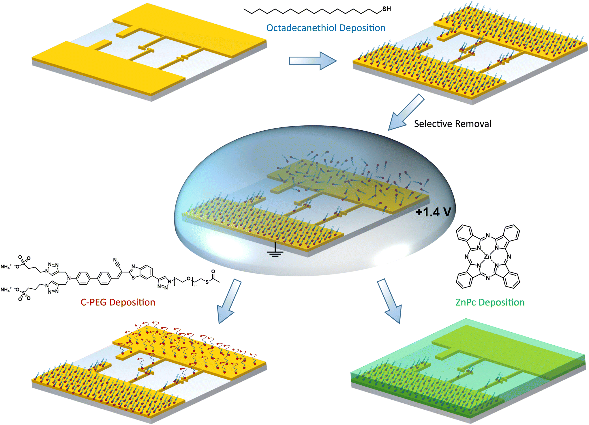 | ||
| Fig. 1 Illustration of site-selective functionalization. First, the sample (with different micro- and nanoelectrodes) is completely covered with 1-octadecanethiol (C18-SH). Then, a droplet of KOH/n-butanol is applied and molecules are removed from the biased electrode via oxidative desorption. A different SAM, e.g. a chromophore containing PEG (C-PEG), is deposited on the liberated electrode, while the C18-SH SAM still covering the opposite electrode acts as a blocking layer. Alternatively, an organic semiconductor, here zinc phthalocyanine, is evaporated onto the asymmetric antenna arrangement to study interface modifications introduced by C18-SH. | ||
As the oxidized species have a considerably reduced affinity to gold surfaces, the method is less prone to issues and artifacts arising from readsorbed molecules.27–29 This is the key feature for nano-sized objects, as already a few readsorbed molecules might have a strong impact on the overall surface properties. By utilizing the steric hindrance imposed by long-chain alkanethiols, such as 1-octadecanethiol (C18-SH), a second SAM based e.g. on a chromophore containing PEG (C-PEG) is deposited on the stripped/uncovered electrode. In order to verify the successful site-selective functionalization, we map the surface coverage by KPFM and photoluminescence measurements. In addition, we demonstrate that the electronic properties of metal–organic interfaces can be tuned on the nanoscale by assembling a functionalized hybrid antenna structure covered by the prototypical organic semiconductor zinc phthalocyanine (ZnPc). Our technique enables the fabrication of nano-optoelectronic devices with advanced functionalities and oriented molecular assemblies, aiming for the overall goal to integrate molecular machinery into metallic nanoelectrodes.
Results and discussion
In Fig. 2a, the asymmetric functionalization of a plasmonic nanoantenna by site-selective removal of a chemisorbed SAM is illustrated. A representative SEM image is shown in Fig. 2b comprising a pair of electrically connected arms separated by a 30 nm gap, whose wiring allows us to apply a voltage between both nanoelectrodes. In a first step, C18-SH, known as a reference for densely packed SAM formation,2 is deposited onto the gold surface from ethanolic solution. For the selective electrochemical removal of the SAM, 0.1 mM solution of potassium hydroxide (KOH) in n-butanol is drop-casted on the sample and a DC voltage of +1.4 V is applied to the left antenna electrode for 30 s. As a result, the gold–thiol bonds on this electrode are broken16 and the released molecules are rinsed off with ethanol, while the SAM covering the opposite antenna electrode remains intact and firmly bound. As desorbed molecules may remain close to the surface,18,27 the rinsing step is crucial and the solvent should be adjusted to fit the SAM's polarity and solubility. The applied voltage can be cycled to improve overall removal of molecules; however, the associated risk of gold surface oxidation may lead to inferior adsorption of a second SAM.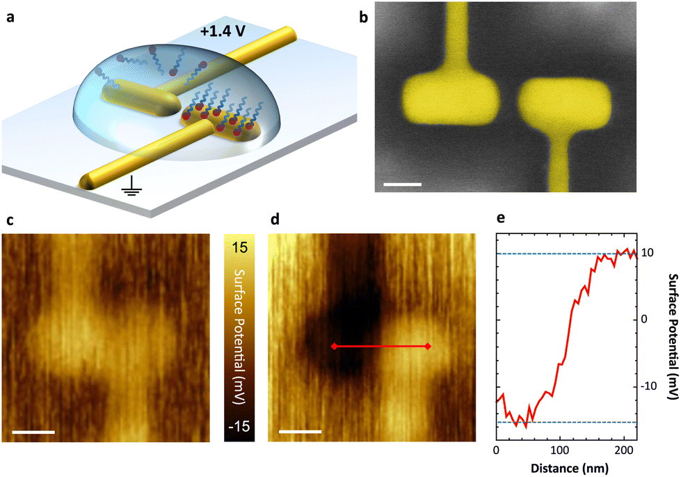 | ||
| Fig. 2 Oxidative desorption at the nanoscale. (a) Schematic of molecule removal from one arm of an electrically-connected nanoantenna upon applying +1.4 V in KOH/n-butanol. (b) SEM image of an exemplary plasmonic nanoantenna with a gap of 30 nm. Scale bar 50 nm. (c) and (d) KPFM images of a plasmonic nanoantenna (c) after deposition of C18-SH and (d) after selectively removing the SAM from the left arm. Scale bars 100 nm. The fast scan direction is bottom to top. (e) Cross-section along the red line in (d) showing an effective surface potential (SP) difference of 25 mV between the two antenna arms. | ||
In order to verify the site-selective functionalization at the nanoscale, we look for the modification of the surface dipole upon adsorption of the SAM. This change is dominated by the effective interface dipole moment of the monolayer (with negligible contribution from the gold–sulfur interaction) which is determined by the strength and orientation of the molecules’ dipole moment and the SAM density. An altered surface dipole will lead to a shift of the vacuum energy level and, thus, an increase or decrease of the gold-SAM electrode work function, depending on the direction of the SAM dipole moment. For example, CH3-terminated alkanethiols reduce the work function (compared to a pure gold (111) surface) as their dipole points towards the surface, while their CF3-terminated analogues lead to the opposite effect.7,30–32 We are able to observe and to qualify this effect with KPFM, which maps the effective surface potential (SP) - a measure correlated to the work function difference of sample and probe tip.21 This allows us to measure variations induced by different molecular coverage.
KPFM images of an antenna before and after site-selective desorption of molecules is shown in Fig. 2c and d. Both antenna arms have the same effective SP after deposition of a homogeneous C18-SH SAM (see Fig. 2c). Upon selective removal from the left antenna arm, KPFM reveals a clear contrast (see Fig. 2d). In this case a nominal SP difference of 25 mV between the two electrodes can be observed (see Fig. 2e). This indicates that only the right antenna electrode and its connector are still covered by an intact SAM. We note that the measured shift is far below values measured by ultraviolet-photoelectron spectroscopy in vacuum.33 This is attributed to the following experimental challenges: (I) the large size of the platinum–iridium KPFM probe tip limits spatial resolution and measurable SP contrast. The 50 nm diameter of the tip is larger than the antenna gap, and thus the tip collects signal from both antenna electrodes while scanning across the gap. (II) Imaging is carried out under ambient conditions; hence, a water layer forms on the uncovered gold surface and induces a dipole moment, which is parallel to the SAM dipole on the covered gold surface.34 (III) The antenna surface is not perfectly flat after focused ion beam milling, which leads to distortion of the SAM in respect of packing and alignment. While the last two points cannot be discriminated in our current setup, we account for probe related artifacts by calibration. A set of known voltages is applied across the electrodes during KPFM and, thereby, we obtain a corrected SP contrast of 200 mV for asymmetric functionalization with C18-SH (see ESI†). We believe this to be the upper limit for measuring SP contrast in this experiment due to the influence of water adsorption and non-perfect surface topographies.
As our method allowed for simple and selective removal of C18-SH SAMs from micro- and nanoscopic electrodes, we were eager to investigate its applicability towards more complex molecules. The highly hydrophilic C-PEG which combines the well-studied PEG chains with a chromophore was chosen as a suitable candidate for this purpose (see Fig. 1).35 A dodecaethyleneglycol chain with a protected terminal thiol group is intended to act as an anchor to the gold (111) surface. The long chain ensures sufficient emitter-metal distance and minimizes quenching once the molecules are immobilized upright standing on the gold.36 The dye can be excited at 532 nm and has a broad emission in the red spectral regime. By using C-PEG, we obtain an optical feedback on larger microelectrodes via fluorescence and can demonstrate that most molecules are removed from the surface upon oxidative desorption.
In order to immobilize C-PEG on the gold surface, it is dissolved in methanol and the masked thiols are deprotected by adding a droplet of 5.4 M NaOMe solution. Next, the substrate is immersed in the solution for 20 minutes resulting in a homogeneous light-emitting SAM in the subsequent PL studies. In Fig. 3a, the direct removal of C-PEG is demonstrated for a substrate with two microscopic electrodes milled into a mono-crystalline gold (111) platelet. C-PEG desorption from the top electrode is carried out as described above for C18-SH, but 0.1 mM KOH in water is used to ensure the solubility of C-PEG. Next, we record a hyperspectral photoluminescence (PL) map showing almost no light emission from that electrode surface, verifying that the C-PEG SAM is indeed removed, while PL is still observed from the opposite electrode. Some molecules remain at the edges of the stripped electrode owing to the large amount of surface defects. In addition, we observe a small unintended desorption from the other gold electrode surface. This is attributed to unstable SAM formation of the PEG chains and hence, solvents with high affinity for the molecules, e.g. dimethyl sulfoxide and water can easily wash the SAM away (even without applied voltage). Still, this method is suitable for the removal of hydrophilic molecules; even at the nanoscale as shown in the ESI.†
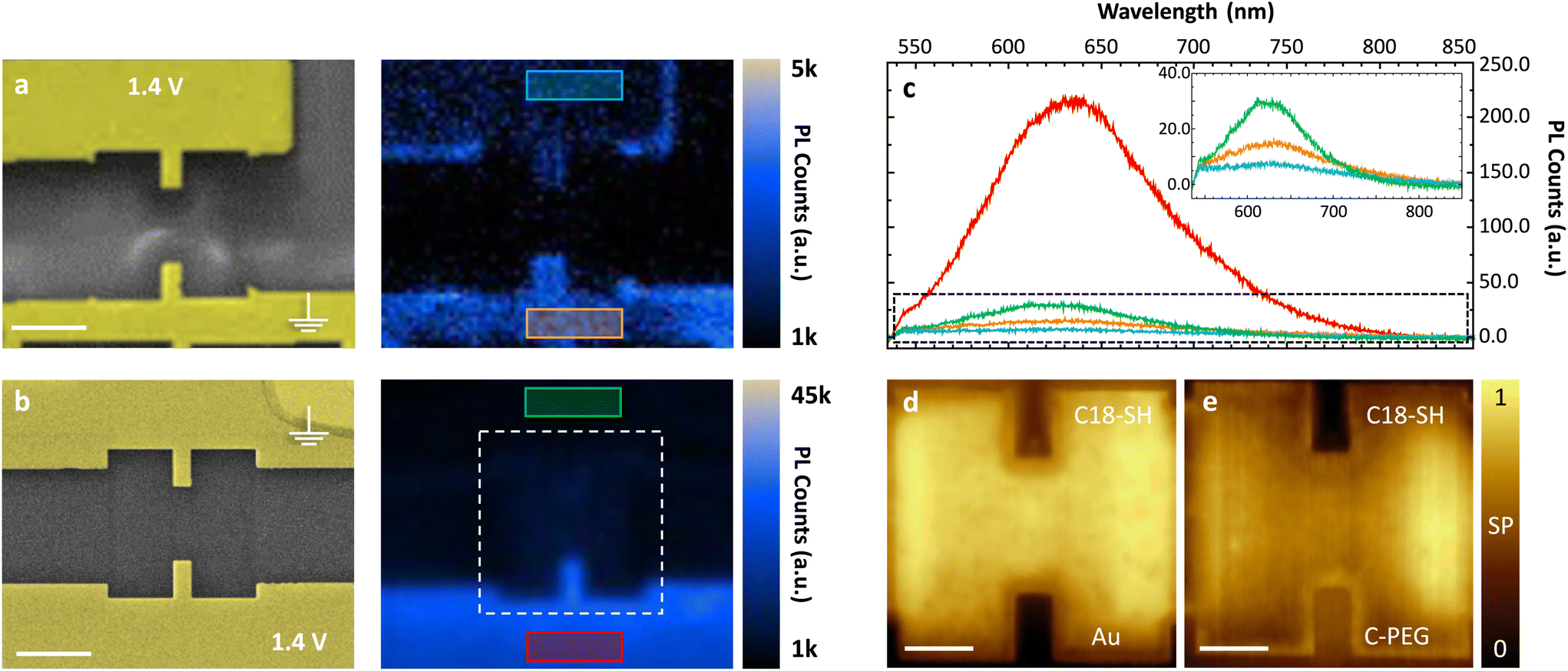 | ||
| Fig. 3 Site-selective functionalization with light-emitting SAM. (a) and (b), Left: SEM images of two microelectrodes. Right: Hyperspectral PL maps of the same electrodes after selective functionalization. Each pixel contains a spectrum, which is integrated to give the total PL counts. Scale bars 2 μm. (a) Direct desorption of C-PEG. After molecule deposition, a DC voltage of +1.4 V is applied to the top electrode, while the other electrodes are grounded. (b) C18-SH is first deposited as a blocking layer and selectively removed by applying +1.4 V to the bottom electrode. Subsequently, C-PEG is deposited and binds to the bottom electrode. (c) Measured spectra recorded by averaging all pixels in the colored rectangles of (a) and (b). The inset shows a zoom into the spectra (black dashed rectangle). (d) and (e) Normalized KPFM images of the marked area in (b; white rectangle) taken (d) after site-selective desorption of C18-SH and (e) after subsequent deposition of C-PEG on the liberated electrode. The surface coverage is denoted. Scale bars 1 μm. | ||
In order to protect C-PEG against any other solvent, we modified the procedure: First, C18-SH is deposited onto the substrate and selectively removed from one of the electrodes. Next, we add C-PEG as described above. Consequently, C18-SH acts as a blocking layer and our target molecule mainly binds to the uncovered electrode. As depicted in Fig. 3b, this method results in a high-quality, unperturbed SAM with homogeneous light emission on the bottom electrode of a second sample. The other electrode, instead, is still covered with C18-SH, and thus almost no emission from the flat surface is observed. Spectra directly extracted from the hyperspectral PL maps allow for further comparison between the two approaches for site-selective functionalization (see Fig. 3c). Minimal light emission from the surface covered with C18-SH is detected (green) as a result of competitive SAM formation. However, emission from the surface without blocking layer (red) is much stronger and significantly exceeds the one obtained in Fig. 3a, indicating that direct removal leads to partial desorption of the C-PEG SAM at the opposite electrode. To further verify the homogeneous coverage of surfaces with C18-SH and C-PEG, we record KPFM maps of an exemplary stripe-electrode. The image in Fig. 3d is taken after removing the blocking layer and displays the expected uniform contrast between covered and uncovered electrode surfaces. This contrast is reversed upon formation of the subsequent C-PEG SAM (see Fig. 3e) owing to its strong dipole moment. We can deduce that the latter is oriented parallel to the dipole moment of C18-SH and has a larger absolute value, thus leading to a stronger SP shift.30,31,33
According to these results we conclude that (I) a significant portion of alkanethiol molecules is removed upon oxidative desorption; (II) the use of a blocking layer is beneficial, and therefore the preferred method for asymmetric functionalization by unstable SAMs, which can easily be desorbed from the surface (e.g. C-PEG); (III) the very low electrolyte concentration does not noticeably oxidize the surface as this would hamper the formation of an additional SAM and (IV) an unintended SAM removal via reductive desorption is not observed.
Next, we demonstrate the feasibility to selectively modify metal–organic interfaces in a nanoscale device. A schematic of the structure and an exemplary SEM image are depicted in Fig. 4a. We employ a stack arrangement similar to that in organic light emitting antennas (OLEAs)24 and functionalize only one of the electrodes by C18-SH. Finally, we vacuum deposit a 30 nm thick layer of the organic semiconductor zinc phthalocyanine (ZnPc; green) on top of the antenna configuration. ZnPc grains around and atop the antenna are visible in the SEM image. The resulting energy diagram for the antenna electrodes with and without C18-SH is illustrated in Fig. 4b. Note, ZnPc deposited on clean gold (111) surfaces, e.g. the stripped antenna electrode, is characterized by preferential hole injection due to the smaller injection barrier.24 As mentioned before, the presence of the alkanethiol SAM shifts the vacuum energy at the Au-SAM-ZnPc boundary and consequently lowers HOMO and LUMO levels of ZnPc relative to the metal work function. In contrast, the stripped (uncovered) electrode experiences only a small shift of the vacuum energy due to a weaker interface dipole at the Au-ZnPc boundary. Hence, the antenna electrodes exhibit selectively modified injection barriers for electrons and holes. The change in morphology of ZnPc grown on top of a SAM covered electrode versus that on a pure gold surface can further influence charge carrier injection.5 We investigate the effect of asymmetric functionalization by recording current–voltage characteristics of several devices. In these measurements, functionalized electrodes are grounded and the voltage is applied to the stripped antenna arm (cf.Fig. 4a). As shown in Fig. 4c and d, all five devices exhibit asymmetric IV-curves, i.e. higher currents at positive voltages, which is in line with a reduced injection barrier for electrons and an increased injection barrier for holes at the SAM-functionalized antenna electrode. Small current variations for different antennas are attributed to slight variations at the metal–organic boundaries. On the other hand, antennas featuring SAMs on both electrodes have symmetric IV-curves (see ESI†). Hence, this experiment is a further proof that we can selectively cover specific nanoscale electrodes and thereby tune the electronic and presumably also structural interface properties of more advanced nanodevices.
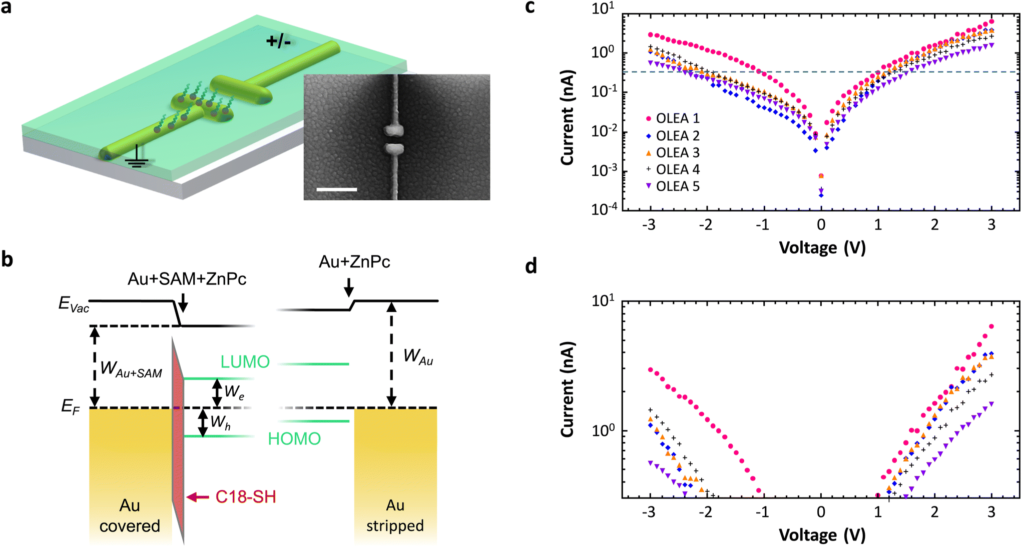 | ||
| Fig. 4 Tuning the gold-organic interface. (a) Schematic of metal–organic nanoantenna with asymmetric functionalization. After C18-SH is removed from one electrode, ZnPc (green) is evaporated. Inset: SEM image of a finalized antenna structure. The bottom arm is covered with C18-SH. The granular texture of the film is caused by ZnPc domains formed upon deposition. Scale bar 300 nm. (b) Energy diagram of the two electrodes with and without C18-SH SAM. ZnPc evaporated on clean gold exhibits a smaller injection barrier for holes than for electrons. The interface dipole introduced by the SAM shifts the vacuum energy level EVac and lowers the HOMO and LUMO levels relative to the metal work function WAu (identified by the Fermi energy EF). As a consequence, injection barriers for electrons (We) and holes (Wh) are selectively modified. Note, the Au-ZnPc boundary also exhibits a small interface dipole. (c) Absolute current as a function of applied voltage for five different devices (with similar dimensions). (d) Zoom-in to the region above the dashed line in (c). The higher currents obtained for positive voltages indicate the asymmetric injection behavior of the selectively functionalized antenna contacts. In all measurements, the SAM-functionalized electrode is grounded. | ||
Conclusions
In summary, we demonstrated an easy-to-use and straightforward technique for site-selective functionalization of micro- and nanoelectrodes with ultra-small dimensions, such as optical antennas. Instead of relying on complicated optical setups, our technique is based on simple oxidative desorption making use of the low probability for readsorption. Surfaces are covered with C18-SH as well as fluorescent C-PEG and asymmetric functionalization is carried out either by direct removal of the previously chemisorbed SAM or by using C18-SH as a blocking layer. The latter is especially beneficial for SAMs which are unstable upon exposure to a highly affine solvent. KPFM and photoluminescence measurements confirm that a significant portion of molecules is desorbed without strongly oxidizing the gold surface. Additionally, we apply our method to selectively modify interface properties of metal–organic nanoantennas, further demonstrating the potential for future nano-optoelectronic devices. By using SAMs with tailored dipole moments and even photoswitchable units,8,38,39 the precise engineering of structural as well as electronic interface properties of nanoscale objects seems feasible in the future. This might pave the road not only towards functional (opto-)electronic nanodevices, but also to the integration of artificial molecular machinery between metallic nanoelectrodes. Once immobilized with a clearly defined orientation, such molecules can perform defined and directed motions controlled by the nanoelectrodes.35Experimental
Materials and methods
SAMs of octadecanethiol are prepared by adding 12 mg of molecules (O1858, Sigma-Aldrich) to 15 mL of absolute ethanol. After the mixture is sonicated for ten minutes, the sample is immersed in the solution and the container is backfilled with nitrogen. The typical incubation time is 24 hours. Eventually, the sample is taken out of the solution, rinsed with absolute ethanol (to remove excess molecules) and dried with a stream of nitrogen.
SAMs of C-PEG are prepared by adding a few grains of molecules to 2 mL of methanol. The solution is sonicated until all molecules are dissolved. In order to deprotect the thiol group, one droplet of sodium methoxide (5.4 m, Acros Organics) is added and the sample is immersed immediately for 20 minutes. Afterwards, the sample is rinsed with purified water and dried with a stream of nitrogen.
ZnPc is evaporated at a rate of 10–15 Ångström per minute (controlled via quartz crystal oscillator) in a high-vacuum multi-chamber system that operates at a base pressure of 10−8 mbar.
Author contributions
M. O. and L. J. conceived the individual experiments. M. E. fabricated evaporated electrode structures and transferred gold platelets. M.O. fabricated optical nanoantennas as well as microelectrodes. L. J. synthesized C-PEG. M. O. performed site-selective functionalization, KPFM, photoluminescence and current–voltage measurements. M. R. vacuum deposited ZnPc. M. O., L. J., J. P., M. M. and B. H. analyzed the data and co-wrote the manuscript. R. K., J. P., M. M. and B. H. supervised the project.Conflicts of interest
There are no conflicts to declare.Acknowledgements
Generous financial support by the Volkswagen-Stiftung (Az. 93438) as well as by the German Research Foundation (projects HE 5618/8-1 and PF385/12-1) is acknowledged. J.P. appreciates financial support by the Bavarian State Ministry of Science, Research, and the Arts (Collaborative Research Network “Solar Technologies Go Hybrid”).References
- F. Schreiber, Prog. Surf. Sci., 2000, 65, 151–257 CrossRef CAS.
- C. Vericat, M. E. Vela, G. Benitez, P. Carro and R. C. Salvarezza, Chem. Soc. Rev., 2010, 39, 1805–1834 RSC.
- Y. J. Du and J. L. Brash, J. Appl. Polym. Sci., 2003, 90, 594–607 CrossRef CAS.
- J. C. Love, L. A. Estroff, J. K. Kriebel, R. G. Nuzzo and G. M. Whitesides, Chem. Rev., 2005, 105, 1103–1170 CrossRef CAS PubMed.
- S. Casalini, C. A. Bortolotti, F. Leonardi and F. Biscarini, Chem. Soc. Rev., 2017, 46, 40–71 RSC.
- P. Stoliar, R. Kshirsagar, M. Massi, P. Annibale, C. Albonetti, D. M. de Leeuw and F. Biscarini, J. Am. Chem. Soc., 2007, 129, 6477–6484 CrossRef CAS PubMed.
- B. de Boer, A. Hadipour, M. M. Mandoc, T. van Woudenbergh and P. W. M. Blom, Adv. Mater., 2005, 17, 621–625 CrossRef CAS.
- M. A. Bartucci, J. Florián and J. W. Ciszek, J. Phys. Chem. C, 2013, 117, 19471–19476 CrossRef CAS.
- S. Erbas-Cakmak, D. A. Leigh, C. T. McTernan and A. L. Nussbaumer, Chem. Rev., 2015, 115, 10081–10206 CrossRef CAS PubMed.
- I. Aprahamian, ACS Cent. Sci., 2020, 6, 347–358 CrossRef CAS PubMed.
- T. Mosciatti, P. Greco, T. Leydecker, M. Eredia, F. Biscarini and P. Samorì, ACS Omega, 2017, 2, 3502–3508 CrossRef CAS PubMed.
- R. D. Piner, J. Zhu, F. Xu, S. Hong and C. A. Mirkin, Science, 1999, 283, 661–663 CrossRef CAS PubMed.
- J. Rundqvist, J. H. Hoh and D. B. Haviland, Langmuir, 2006, 22, 5100–5107 CrossRef CAS PubMed.
- S. Friebel, J. Aizenberg, S. Abad and P. Wiltzius, Appl. Phys. Lett., 2000, 77, 2406–2408 CrossRef CAS.
- S. Simoncelli, Y. Li, E. Cortés and S. A. Maier, ACS Nano, 2018, 12, 2184–2192 CrossRef CAS PubMed.
- C. A. Widrig, C. Chung and M. D. Porter, J. Electroanal. Chem. Interfacial Electrochem., 1991, 310, 335–359 CrossRef CAS.
- T. Kawaguchi, H. Yasuda, K. Shimazu and M. D. Porter, Langmuir, 2000, 16, 9830–9840 CrossRef CAS.
- E. Pensa, C. Vericat, D. Grumelli, R. C. Salvarezza, S. H. Park, G. S. Longo, I. Szleifer and L. P. M. D. Leo, Phys. Chem. Chem. Phys., 2012, 14, 12355–12367 RSC.
- E. H. J. Wong, G. L. May and C. P. Wilde, Electrochim. Acta, 2013, 109, 67–74 CrossRef CAS.
- M. Tencer and P. Berini, Langmuir, 2008, 24, 12097–12101 CrossRef CAS PubMed.
- A. Liscio, E. Orgiu, J. M. Mativetsky, V. Palermo and P. Samorì, Adv. Mater., 2010, 22, 5018–5023 CrossRef CAS PubMed.
- C. Wälti, R. Wirtz, W. A. Germishuizen, D. M. D. Bailey, M. Pepper, A. P. J. Middelberg and A. G. Davies, Langmuir, 2003, 19, 981–984 CrossRef.
- J. Kern, R. Kullock, J. Prangsma, M. Emmerling, M. Kamp and B. Hecht, Nat. Photonics, 2015, 9, 582–586 CrossRef CAS.
- P. Grimm, S. Zeißner, M. Rödel, S. Wiegand, S. Hammer, M. Emmerling, E. Schatz, R. Kullock, J. Pflaum and B. Hecht, Nano Lett., 2022, 22, 1032–1038 CrossRef CAS PubMed.
- E. Krauss, R. Kullock, X. Wu, P. Geisler, N. Lundt, M. Kamp and B. Hecht, Cryst. Growth Des., 2018, 18, 1297–1302 CrossRef CAS.
- X. Wu, R. Kullock, E. Krauss and B. Hecht, Cryst. Res. Technol., 2015, 50, 595–602 CrossRef CAS.
- A. Musgrove, A. Kell and D. Bizzotto, Langmuir, 2008, 24, 7881–7888 CrossRef CAS PubMed.
- R. L. Garrell, J. E. Chadwick, D. L. Severance, N. A. McDonald and D. C. Myles, J. Am. Chem. Soc., 1995, 117, 11563–11571 CrossRef CAS.
- M. H. Schoenfisch and J. E. Pemberton, J. Am. Chem. Soc., 1998, 120, 4502–4513 CrossRef CAS.
- P. C. Rusu and G. Brocks, J. Phys. Chem. B, 2006, 110, 22628–22634 CrossRef CAS PubMed.
- R. W. Zehner, B. F. Parsons, R. P. Hsung and L. R. Sita, Langmuir, 1999, 15, 1121–1127 CrossRef CAS.
- J. Pflaum, G. Bracco, F. Schreiber, R. Colorado, O. E. Shmakova, T. R. Lee, G. Scoles and A. Kahn, Surf. Sci., 2002, 498, 89–104 CrossRef CAS.
- D. M. Alloway, M. Hofmann, D. L. Smith, N. E. Gruhn, A. L. Graham, R. Colorado, V. H. Wysocki, T. R. Lee, P. A. Lee and N. R. Armstrong, J. Phys. Chem. B, 2003, 107, 11690–11699 CrossRef CAS.
- R. L. Wells and T. Fort, Surf. Sci., 1972, 32, 554–560 CrossRef CAS.
- L. Jucker, M. Ochs, R. Kullock, Y. Aeschi, B. Hecht and M. Mayor, Org. Mater., 2022, 4, 127–136 CrossRef CAS.
- Y. S. Chi, H. R. Byon, B. S. Lee, B. Kong, H. C. Choi and I. S. Choi, Adv. Funct. Mater., 2008, 18, 3395–3402 CrossRef CAS.
- R. Kullock, M. Ochs, P. Grimm, M. Emmerling and B. Hecht, Nat. Commun., 2020, 11, 115 CrossRef CAS PubMed.
- N. Crivillers, S. Osella, C. Van Dyck, G. M. Lazzerini, D. Cornil, A. Liscio, F. Di Stasio, S. Mian, O. Fenwick, F. Reinders, M. Neuburger, E. Treossi, M. Mayor, V. Palermo, F. Cacialli, J. Cornil and P. Samorì, Adv. Mater., 2013, 25, 432–436 CrossRef CAS PubMed.
- D. A. Egger, F. Rissner, G. M. Rangger, O. T. Hofmann, L. Wittwer, G. Heimel and E. Zojer, Phys. Chem. Chem. Phys., 2010, 12, 4291–4294 RSC.
Footnotes |
| † Electronic supplementary information (ESI) available: Additional measurements and discussion thereof, KPFM correction, symmetric metal–organic nanoantennas. See DOI: https://doi.org/10.1039/d2nr06343c |
| ‡ These authors contributed equally to this work. |
| This journal is © The Royal Society of Chemistry 2023 |