
 Open Access Article
 This Open Access Article is licensed under a Creative Commons Attribution-Non Commercial 3.0 Unported Licence
Homogeneous in-plane WSe2 P–N junctions for advanced optoelectronic devices†
Dewu
Yue
a,
Xin
Ju
*b,
Tao
Hu
a,
Ximing
Rong
 c,
Xinke
Liu
c,
Xiao
Liu
c,
Hong Kuan
Ng
b,
Dongzhi
Chi
b,
Xinzhong
Wang
*a and
Jing
Wu
*bd
c,
Xinke
Liu
c,
Xiao
Liu
c,
Hong Kuan
Ng
b,
Dongzhi
Chi
b,
Xinzhong
Wang
*a and
Jing
Wu
*bd
aInformation Technology Research Institute, Shenzhen Institute of Information Technology, Shenzhen, 518172, China. E-mail: wangxz@sziit.com.cn
bInstitute of Materials Research and Engineering (IMRE), Agency for Science, Technology and Research (A*STAR), 2 Fusionopolis Way, Innovis #08-03, Singapore 138634, Singapore. E-mail: ju_xin@imre.a-star.edu.sg; wujing@imre.a-star.edu.sg
cCollege of Materials Science and Engineering, Shenzhen Key Laboratory of Special Functional Materials, Shenzhen Engineering Laboratory for Advanced Technology of Ceramics, Guangdong Research Center for Interfacial Engineering of Functional Materials, Shenzhen University, Shenzhen 518060, China
dDepartment of Materials Science and Engineering, National University of Singapore, 9 Engineering Drive 1, Singapore 117575, Singapore
First published on 25th January 2023
Abstract
Conventional doping schemes of silicon (Si) microelectronics are incompatible with atomically thick two-dimensional (2D) transition metal dichalcogenides (TMDCs), which makes it challenging to construct high-quality 2D homogeneous p–n junctions. Herein, we adopt a simple yet effective plasma-treated doping method to seamlessly construct a lateral 2D WSe2 p–n homojunction. WSe2 with ambipolar transport properties was exposed to O2 plasma to form WOx on the surface in a self-limiting process that induces hole doping in the underlying WSe2via electron transfer. Different electrical behaviors were observed between the as-exfoliated (ambipolar) region and the O2 plasma-treated (p-doped) region under electrostatic modulation of the back-gate bias (VBG), which produces a p–n in-plane homojunction. More importantly, a small contact resistance of 710 Ω μm with a p-doped region transistor mobility of ∼157 cm2 V−1 s−1 was achieved due to the transformation of Schottky contact into Ohmic contact after plasma treatment. This effectively avoids Fermi-level pinning and significantly improves the performance of photodetectors. The resultant WSe2 p–n junction device thus exhibits a high photoresponsivity of ∼7.1 × 10⁴ mA W−1 and a superior external quantum efficiency of ∼228%. Also, the physical mechanism of charge transfer in the WSe2 p–n homojunction was analyzed. Our proposed strategy offers a powerful route to realize low contact resistance and high photoresponsivity in 2D TMDC-based optoelectronic devices, paving the way for next-generation atomic-thickness optoelectronics.
 Jing Wu | Dr Jing Wu received his bachelor's degree in Physics from Zhejiang University in 2010 and his PhD in physics from the National University of Singapore (NUS) in 2015. He is currently the group leader of the Nano Electronic and Thermal Transport (NETT) group at the Institute of Materials Research and Engineering (IMRE) and an adjunct faculty member in the Department of Materials Science and Engineering, NUS. His research interests focus on the exotic transport dynamics and scattering physics of 2D materials, such as charge transport, thermoelectric and optoelectronic transport, and exploring the technical aspects for high-performance electronics. |
1. Introduction
Two-dimensional (2D) materials, such as transition metal dichalcogenides (TMDCs), hold promise as fundamental building blocks for next-generation flexible electronic and optoelectronic devices because of their tunable bandgap, high mobility, good chemical stability, and ability to form high-quality interfaces in van der Waals (vdW) heterostructures.1–5 Among all TMDCs, WSe2 is an intriguing 2D material that offers bipolar transport characteristics with thickness-dependent band gaps of 1.7 eV (direct, monolayer) and approximately 1.2 eV (indirect, multilayer), as well as theoretical electron and hole motilities of about 250 and 270 cm2 V−1 s−1, respectively.6–8 Owing to its unique physical properties, WSe2 has opened the door to versatile electronic and optoelectronic devices with excellent optoelectronic performance. In recent years, new artificial structures based on van der Waals (vdW) vertical heterostructures or lateral p–n heterojunctions have attracted great interest in the application of WSe2 optoelectronic devices.9–14 For instance, Jo and co-workers demonstrated that the photoresponsivity of WSe2/h-BN-based p–n heterojunction photodetectors was remarkably improved by a triphenylphoshine n-doping method.15 Guo and co-workers reported that a WSe2–ZnO p–n heterojunction photodetector fabricated by combining p-type WSe2 and n-type ZnO exhibited an ultra-high photoresponsivity of 4.83 × 10³ A W−1 under 405 nm light illumination.16 Liu et al. reported that a photodetector based on a WSe2–Bi2Te3 p–n heterojunction can give rise to a fast response time of ∼210 μs and a high photoresponsivity of ∼20.5 A W−1 under 633 nm illumination.17 These results have demonstrated that the successful construction of heterojunctions can significantly improve the photoresponse characteristics of TMDC-based devices, which, however, still suffer from unavoidable residues and complex flake alignment processes, i.e., difficult to localize the target material onto another flake accurately.18 In addition, the presence of a vdW gap between junctions may inhibit carrier charge transfer, which is generally undesirable for the device performance. As an alternative strategy, homogeneous junctions offer intrinsic advantages over heterogeneous junctions by providing clean and self-aligned interfaces.Since the Fermi level (EF) of WSe2 resides in the middle of the band gap, its ambipolar nature allows for electron or hole dominant transport via selective doping, which can be used as an ideal candidate for the implementation of p–n photodiodes, photovoltaic cells, and complementary logic systems.19–23 However, the in situ synthesis of high-quality homogeneous WSe2 p–n junction-based photodetectors still faces many hurdles, such as the complex fabrication process, slow photoresponsivity, low photodetectivity, etc. On the other hand, the formation of a Schottky barrier (SB) at the WSe2–metal interface inevitably results in a high contact resistance (Rc).24,25 Furthermore, the physical metal deposition process may cause potential lattice disorders or even local destruction of the material, leading to Fermi-level pinning or poor band alignment, ultimately limiting the efficiency of photodiodes.26–28 Consequently, carrier transport can only be carried out by tunneling through thin SBs, resulting in a low current density. To overcome the inherent performance limits of 2D TMDCs and to improve the contact problems on WSe2 functional devices, various doping schemes, work function engineering techniques, electrical tuning techniques, etc. have been explored.29–35 However, these methods are relatively complicated and require high temperature or vacuum process conditions, which greatly hinder their practical application in constructing high-performance WSe2-based photodetectors. Most recently, transition metal oxides (TMOs) used in organic electronics and 2D material-based electronic devices have been demonstrated as effective p-type contacts and dopants.36,37 This doping scheme has been widely developed and applied in complementary metal–oxide–semiconductor (CMOS) technology. Despite many encouraging outcomes so far, the fabrication of a 2D TMDC p–n homojunction with low Rc is still limited by technical challenges.
In this work, we demonstrate an efficient and reliable approach by performing O2 plasma treatment to easily permit the amplification of hole transport, and thus achieve in situ p-type semiconductor characteristics in WSe2. The under-stoichiometric oxidation of WSe2 into WOx highly induces hole doping in the neighboring (or underlying) WSe2via electron transfer from the underlying WSe2 to the top oxidized WOx layer. Moreover, our results revealed that the transformation of the SB to Ohmic contact arising from plasma treatment greatly increases the hole mobility from ∼22 to ∼157 cm2 V−1 s−1 in a p-type doped WSe2 transistor. As a result, the as-fabricated in-plane p–n homojunction exhibits a superior external quantum efficiency of ∼228%, an excellent photoresponsivity of ∼7.1 × 10⁴ mA W−1, and a photodetectivity of ∼3 × 10³ Jones under 532 nm light illumination. The resultant device performance of our method proves it to be an ideal strategy for constructing high-performance p–n junction optoelectronic devices by using self-oxidizing 2D TMDCs, which may be applied to other TMDCs for future multifunctional electronic and optoelectronic applications.
2. Results and discussion
Fig. 1(a) shows the schematic illustration of a pristine and plasma-treated WSe2. The WSe2 flake was treated with physical O2 plasma bombardment where the Se atoms were replaced by O atoms, which then forms a WOx layer on the surface of the WSe2 flake. The same sample was repeatedly subjected to plasma treatment, and the transfer characteristics of the as-fabricated WSe2 FET at cumulative plasma durations of 5 to 120 s were measured (Fig. S1†). A change in the majority of carriers, from electrons to holes (n-dominant ambipolar to strong p-type), is observed with an on/off ratio reaching 108 after 120 s of O2 plasma treatment as shown in Fig. S1.† As a result, the topmost layers of the WSe2 flake were completely oxidized into WOx, consistent with previous reports where WOx is used as an effective doping layer.23 In addition, the thickness of the WSe2 flakes increased by ∼1 nm after O2 plasma treatment (Fig. 1(b)), which is an indication of the formation of a thin layer of WOx atop the WSe2 flake. The oxidation depth of the WSe2 flake was subsequently assessed using the secondary-ion mass spectrometry (SIMS) technique. As shown in Fig. S2,† oxidation is found to be a self-limiting process. The depth of the oxide layer (WOx, including WO−, WO2−, and WO3−) is determined to be approximately 1.2 nm, which is restricted only in the very top layer, therefore offering an easy and efficient control of the oxide thickness. To further validate the formation of the WOx layer, the surface composition of the plasma-treated WSe2 was further analyzed using X-ray photoelectron spectroscopy (XPS), as presented in Fig. 1(c). The XPS core spectrum of the pristine WSe2 shows two main peaks at 27.82 and 31.20 eV corresponding to W 4f7/2 and W 4f5/2, respectively.38,39 In comparison, the W 4f7/2 (28.11 eV) and W 4f5/2 (31.49 eV) peaks of the plasma-treated WSe2 showed a slight shift to higher binding energies. Moreover, a clear additional peak can be observed at the binding energy of 36.50 eV corresponding to WOx (x ≤ 3),40 which verifies the presence of WOx at the top of WSe2 flakes. These results demonstrate that oxygen radicals are efficiently doped into WSe2 crystals during plasma exposure. Furthermore, the transport characteristics of the pristine and plasma-treated WSe2-based FETs were investigated under an applied gate voltage from −60 to 60 V. The optical microphotograph of the plasma treated WSe2 based-FET is presented in the inset of Fig. 1(d). The pristine WSe2-based FET exhibits n-type dominated ambipolar characteristics, as shown in Fig. 1(d). However, after O2 plasma treatment, the transfer curve shows a heavily p-doped characteristic (Fig. 1(d)). These results confirm the modulation of the as-fabricated WSe2 channels with O2 plasma, which act as p-type dopants when exposed to controlled plasma conditions.41 The field-effect mobility (μFE) can be calculated from the following formula μFE = gmLch/CoxWchVSD,42 where Lch and Wch are the channel length and width, respectively, Cox = 1.15 × 10⁻⁸ F cm−2 for 300 nm SiO2, gm = ∂ID/∂VBG is the transconductance, and VSD is the source–drain voltage. The maximum μFE of the as-fabricated WSe2 FETs is found to be about 157 cm2 V−1 s−1, which is much higher than previously reported results (see Table 1). Fig. 1(e) shows the μFE of the pristine and O2-treated WSe2 devices fabricated with different thicknesses from 5 nm to 30 nm, where the FET mobility is significantly increased by up to a factor of 8 after O2 plasma-induced p-type doping. We believe that the high mobility obtained may be attributed to the lowering of the contact resistance (Rc) by plasma doping.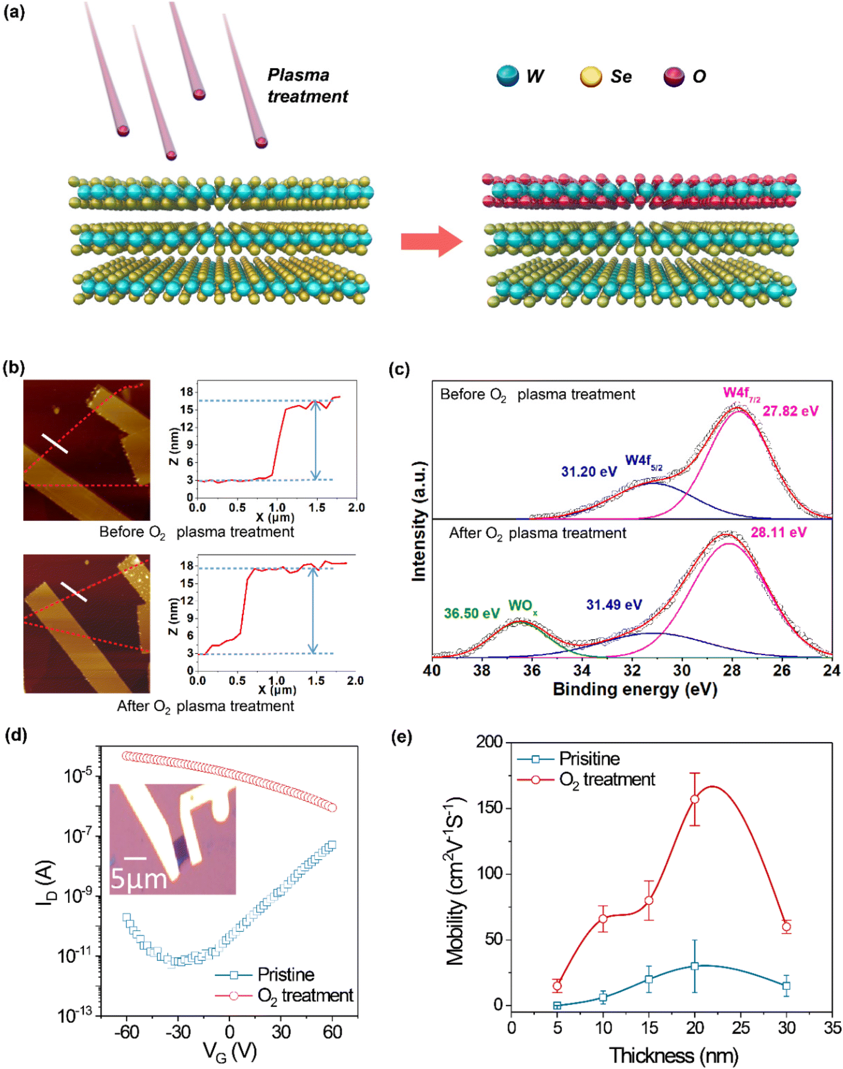 | ||
| Fig. 1 (a) Schematic illustration of O2 plasma treatment of bulk WSe2. (b) The AFM images of a WSe2 flake before and after O2 plasma treatment, and the right part shows the AFM height profile revealing the thickness of the ∼13 nm WSe2 flake. (c) The XPS spectral comparison shows the existence of one extra peak at a binding energy of 36.50 eV corresponding to WOx and a slight shift in the binding energies of W peaks after O2 plasma treatment. (d) Transfer characteristics of a WSe2 FET with Vd = 1 V before and after O2 plasma treatment. The inset shows the optical image of the as-fabricated WSe2 FET. (e) The mobility obtained from WSe2 FETs of different thicknesses. | ||
| Materials | Field-effect mobility (cm2 V−1 s−1) | Ref. |
|---|---|---|
| WSe 2 pn-junction | 157 | This work |
| WSe2/MoS2 heterojunction | 8.42 | 6 |
| WSe2(1−x)Te2x | 46 | 7 |
| WSe2/ReS2 pn-junction | 16.5 | 10 |
| WSe2 pn-junction | 36.28 | 11 |
| Monolayer WSe2 | 132 | 13 |
| WSe2/h-BN heterojunction | 25.6 | 15 |
| WOx/WSe2 heterojunction | 40 | 23 |
| WSe2 flake | 2.2 | 24 |
| WSe2/Graphene heterojunction | 84 | 25 |
| Monolayer WSe2 | 82 | 28 |
| WSe2 flake | 150 | 35 |
It is well-known that a high contact resistance Rc would significantly affect the electrical and optical performances of TMDC-based FETs.30 Hence, we fabricated devices with the same channel width and different channel lengths ranging from 2 to 5 μm to evaluate the contact Rc of the p-doped WSe2 channels by the transmission line method (TLM). Fig. 2(a) shows the optical images of the WSe2 devices with varied channel lengths for examining contact properties. The enlarged schematic in Fig. 2(a) illustrates the carrier pathways (yellow arrows) in the channel of the plasma-treated device, where the electron transfer from the underlying WSe2 to the surface WOx contributes to the formation of electron transport paths (red arrows) from the channel to the doping layer, which is consistent with previous reports.23,43,44 In particular, a thin WOx layer formed after the oxygen plasma treatment will attract electrons from the neighboring (or underlying) WSe2, thereby inducing the heavily p-doped WSe2, i.e., the formation of a conducting channel of holes. The transfer characteristics of these devices are shown in Fig. S3.†Fig. 2(b) and (c) show the output characteristics obtained from the pristine and O2 plasma-treated WSe2-based FETs, respectively. The non-linear increase of hole current with increasing drain bias (VD) indicates a large SB between the metal and pristine WSe2 layers (see Fig. 2(b)). In contrast, the excellent linear characteristics of the output curve of the O2-plasma treated WSe2 layers in Fig. 2(c) suggest the conversion of Schottky contact into Ohmic-like behavior. This may be attributed to the shift of the Fermi level towards the valence band maximum (VBM) of WSe2: p-type dominant conversion. We believe that this phenomenon contributes to the transition from Schottky emission to direct tunneling for easier hole injection. For Schottky emission,45I = ISE![[thin space (1/6-em)]](https://www.rsc.org/images/entities/char_2009.gif) exp(A√V), where ISE and A (>0) are two parameters related to Schottky emission behavior. For F–N tunneling or FNT,46I = IFNV2exp(B/V), where IFN and B (<0) are two parameters related to F–N tunneling behavior. To better elucidate the transition from Schottky emission to direct tunneling, the I–V curves are plotted in the forms of lnI-vs.-V1/2 and ln(I/V2)-vs.-V−1, respectively. Fig. S4† shows that before plasma treatment, the channel is dominated by Schottky emission, while after plasma treatment, the F–N tunneling becomes dominant. To further quantify the variation in Rc after plasma treatment, Fig. 2(d) shows the linear fitting of the total resistance (Rtotal) as a function of channel length (L). Rtotal could be described as Rtotal = LRch/W + 2Rc,47 where Rc is the contact resistance, W is the channel width, L is the channel length, and Rch is the 2D channel resistance. The value of Rc can be directly extracted from the y-intercept of the linear fit to Rtotal. Fig. 2(e) shows Rc ranging from 0.71 to 6.73 kΩ μm under different gate voltages ranging from −60 to 60 V. Considering the small thickness of the channel, uniform doping leads to a uniform current distribution in the vertical direction. A high gate bias leads to an increase in carrier density and the narrowing of the potential barrier along the metal and the material interface. The elevated hole concentration and narrowed potential barrier aid in the injection of carriers into the WSe2 channel and thereby achieve a transition from Schottky emission to direct tunneling. As a result, a lower contact resistance is obtained.47 In particular, the lowest Rc of ∼710 Ω μm measured at VBG = −60 V can be successfully achieved in the plasma-treated WSe2 FETs, suggesting a reduction in Rc after the plasma treatment. It should be noted that such a small Rc highlights the importance of the self-terminating oxidation process, resulting in the thinnest oxide and therefore a transparent tunnel barrier for increased hole injection between the metal and WSe2 as a key factor for the excellent device performance.
exp(A√V), where ISE and A (>0) are two parameters related to Schottky emission behavior. For F–N tunneling or FNT,46I = IFNV2exp(B/V), where IFN and B (<0) are two parameters related to F–N tunneling behavior. To better elucidate the transition from Schottky emission to direct tunneling, the I–V curves are plotted in the forms of lnI-vs.-V1/2 and ln(I/V2)-vs.-V−1, respectively. Fig. S4† shows that before plasma treatment, the channel is dominated by Schottky emission, while after plasma treatment, the F–N tunneling becomes dominant. To further quantify the variation in Rc after plasma treatment, Fig. 2(d) shows the linear fitting of the total resistance (Rtotal) as a function of channel length (L). Rtotal could be described as Rtotal = LRch/W + 2Rc,47 where Rc is the contact resistance, W is the channel width, L is the channel length, and Rch is the 2D channel resistance. The value of Rc can be directly extracted from the y-intercept of the linear fit to Rtotal. Fig. 2(e) shows Rc ranging from 0.71 to 6.73 kΩ μm under different gate voltages ranging from −60 to 60 V. Considering the small thickness of the channel, uniform doping leads to a uniform current distribution in the vertical direction. A high gate bias leads to an increase in carrier density and the narrowing of the potential barrier along the metal and the material interface. The elevated hole concentration and narrowed potential barrier aid in the injection of carriers into the WSe2 channel and thereby achieve a transition from Schottky emission to direct tunneling. As a result, a lower contact resistance is obtained.47 In particular, the lowest Rc of ∼710 Ω μm measured at VBG = −60 V can be successfully achieved in the plasma-treated WSe2 FETs, suggesting a reduction in Rc after the plasma treatment. It should be noted that such a small Rc highlights the importance of the self-terminating oxidation process, resulting in the thinnest oxide and therefore a transparent tunnel barrier for increased hole injection between the metal and WSe2 as a key factor for the excellent device performance.
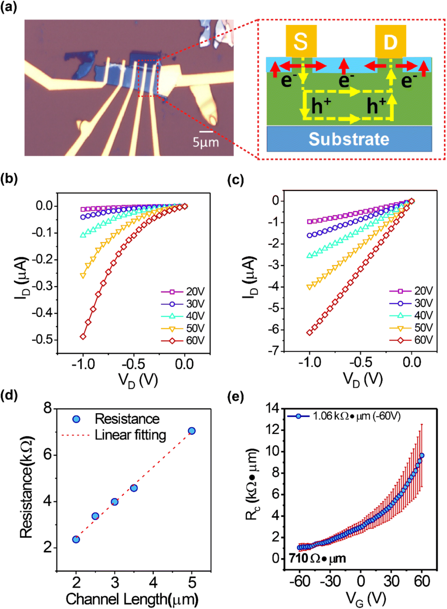 | ||
| Fig. 2 Contact properties of the WSe2 FETs obtained by TLM measurement. (a) Optical micrograph of the TLM devices. The enlarged section on the right side shows the hole transport path occurring in the whole channel, which can lead to low contact resistance and thus higher mobility. (b) Schottky contact can be clarified from the output characteristics of the pristine WSe2 FETs. (c) By applying O2 plasma treatment, Ohmic contact was achieved in WSe2 FETs. (d) Rtotal as a function of channel length to extract Rc using a TLM linear fitting curve. (e) Rcversus bottom gate voltage in which the lowest Rc obtained was ∼710 Ω μm at a VBG of −60 V. | ||
The p–n junction is crucial for the separation of photon-induced electron–hole (e–h) pairs towards achieving photodetectors with high responsivity or solar cells with high quantum efficiency.48,49 Through oxidation doping, the partial doping of a WSe2 FET results in a lateral p–n homojunction. To determine their optoelectronic performance, WSe2 lateral junctions were fabricated. More detailed information regarding the device preparation process can be found in the Experimental section. Fig. 3(a) shows the schematic diagram and the optical image (top-view) of the fabricated WSe2 devices. These WSe2 devices were then exposed to O2 plasma under different operating conditions (see the Experimental section). Note that a PMMA layer is employed as a mask to protect areas with electrodes 1 to 2, leaving areas with electrodes marked with 3 to 4 exposed for O2 plasma treatment. The O2 molecule was then chemisorbed onto the top surface of the exposed WSe2, in which the top layer of the Se atom was substituted by an oxygen atom. Finally, the WOx layer was formed on top of the WSe2 layer. As a result of p-doping due to O2 plasma (formation of a WOx layer on the top of WSe2), a p-type (n-type) dominant conduction is observed in the O2 plasma-treated (plasma-protected) region. The typical transfer curves of the pristine WSe2 channel (through electrodes 1 to 2) were measured to maintain n-type behaviour (Fig. 3(b)). The electrical performance of the as-prepared plasma-treated channel was then measured through electrodes 3 to 4 (Fig. 3(c) and Fig. S5†), yielding p-type characteristics. With the capability of achieving both unipolar p-type (plasma-treated) and n-type (pristine) conduction behaviours, a lateral p–n homojunction can then be fabricated using a single WSe2 flake. Fig. 3(d) and (e) show the corresponding Id − Vd output curves of the partially doped WSe2 device (channel: electrodes 2–3) with Vg = −40 V in the linear (left) and log (right) scales, in which little to no current flow is observed under reverse source–drain bias (Vd < 0 V). However, a much higher current flow can be observed when a forward bias is applied (Vd > 0 V), indicating the forward rectifying diode behavior. Furthermore, an ideality factor (n)50,51 of 1.4 was calculated from the dark current (Fig. 3(e)), indicating the formation of a near-ideal p–n junction.52,53 It is known that n = 1 indicates an ideal p–n junction diode, n ranging between 1 and 2 implies the existence of a tunneling current, and n = 2 indicates the existence of defects or interface traps that drives the recombination process.54 Thus, our good ideality factor of ∼1.4 can be ascribed to the low charge trap density at the homojunction interface.55 The above results prove the successful preparation of a p–n junction between electrodes 2 and 3. However, it should be noted that the p–n WSe2 device is formed with a Schottky junction in the n-type part of WSe2 (contact 2), p–n junctions in the channel (electrodes 2–3), and Ohmic-like contact in the p-type part of WSe2 (contact 3).
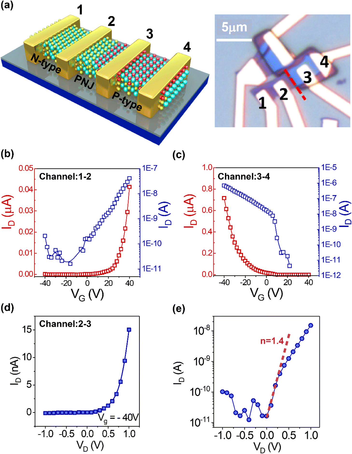 | ||
| Fig. 3 (a) 3D schematic structure and optical photograph (right side) of an O2 plasma-treated WSe2 FET device showing channels 1–2, 2–3, and 3–4 as n-WSe2, pn-WSe2, and p-WSe2, respectively. (b) and (c) The transfer curves of n- and p-WSe2 channels measured at Vd = 1 V after O2 plasma treatment, which are represented in both linear and logarithmic scales. (d) The output curve of an O2 plasma-treated WSe2 p–n junction device obtained at Vg = −40 V is represented on a linear scale. (e) The output curve is represented on a logarithmic scale to calculate the p–n junction ideality factor as 1.4. | ||
Next, we explored the optoelectronic properties of p–n WSe2 homojunction photodetectors. The transfer curves of the as-fabricated photodetector were measured in the dark and 532 nm illumination. By comparison, a photocurrent response characteristic under light irradiation is observed in Fig. 4(a), which may be mainly attributed to the strong light absorption in the WSe2 p–n junction. This then generates a larger density of photoinduced e–h pairs which leads to a reduction of the Schottky barrier, thereby allowing the photogenerated carriers to transmit more effectively along the metal/WSe2 interface under an externally applied bias. To further investigate the performance of WSe2 p–n junction photodetectors and to study their dynamic optical response, time (T)- and gate voltage (VG)-dependent photocurrent measurements under a fixed source–drain bias of 1 V were performed as shown in Fig. 4(b). Here, the time (T)- and source–drain voltage (VD)-dependent photocurrent of the WSe2 p–n junction photodetectors was also measured at the fixed gate bias of 40 V (Fig. 4(c)). As VG swept from +40 to −40 V, the photocurrent enhancement was observed under various VD and VG conditions. In particular, the maximum photocurrent is obtained under a gate bias voltage of 40 V. Meanwhile, prominent variations in the gate-dependent photocurrent can be obtained at both VG < 0 V and VG > 0 V sides. These results suggest that the photocurrent response can be effectively modulated by the gate electric field. In addition, the photocurrent is observed to slightly decrease with time under continuous light irradiation, indicating possible charge trapping effects. Higher gate voltage (40 V) leads to an increase in carrier concentration while the potential barrier at the contact interface becomes narrower. Thus, the charge trap states are relatively more easily filled with carriers, leading to a slight reduction in photocurrent. In contrast, at a gate voltage of 0 V, when the Fermi level is in equilibrium, the carrier density is relatively low. As such, carriers are difficult to be captured by trap states, so minimal photocurrent changes are observed in time-dependent photocurrent measurements (Fig. S6†). The photocurrent characteristics of the junction can be further understood through the energy band diagrams, as shown in Fig. 4(d)–(f). Fig. 4(d) shows the band diagram of the WSe2 p–n junction in the equilibrium state. The Fermi level of the p-type area is near to the valence band, whereas the Fermi level of the n-type part is near to the conduction band. Under reverse bias, the energy barrier at the junction becomes higher as the width of the depletion region increases. Consequently, electrons cannot transmit effectively, and the p–n junction is in the OFF state. Under forward bias, the energy barrier becomes lower, thus allowing electrons to easily pass through the junction, and the p–n junction is in the ON state. This typical p–n junction behavior is consistent with the output curve as shown in Fig. 3(d). Furthermore, the mechanism of photocurrent generated in the dark (Fig. 4(e)) and light (Fig. 4(f)) states was also proposed. When the negative gate voltage is applied in the dark state (Fig. 4(e)), the Fermi level drops below the valence band of the p-type branch, which enables holes to flow easily from the junction into the metal. As a result, there is no current in the p–n junction. When a positive gate voltage is applied, the Fermi level moves into the conduction band in the n-type branch, which allows electrons to easily transfer from the junction into the metal. Therefore, the designed lateral p–n junction shows no current when electrons are dominant carriers. Under light irradiation, the generation of e–h pairs takes place near the depletion region, and the photoexcited carriers are swept from the junction in opposite directions by an externally applied bias, resulting in a net increase in photocurrent, as shown in Fig. 4(f). As a result, internal hole and electron transport combined with the resulting overdose e–h pairs from light absorption increases the current, which is much higher than the dark state (as shown in Fig. 4(e)) even at low gate voltages. In both positive and negative gate biases, the photocurrent is high as the substantial photogenerated e–h pairs can be readily separated and driven toward the cathode and anode contacts in the in situ WSe2 lateral p–n junction.
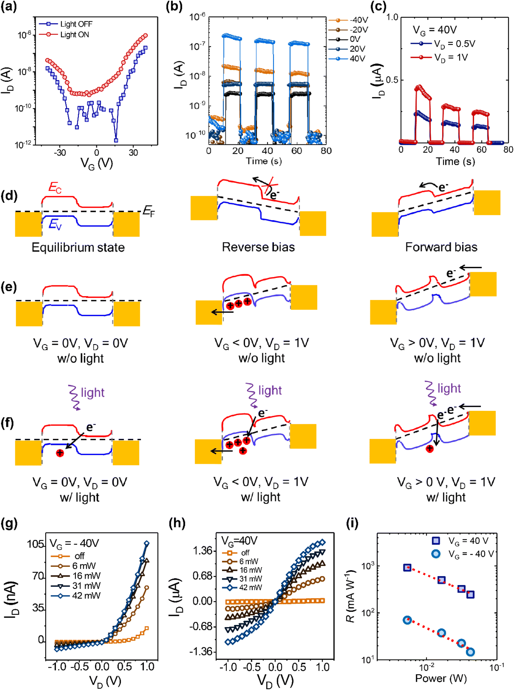 | ||
| Fig. 4 (a) Typical photoresponse of the WSe2 p–n homojunction FET devices under 532 nm illumination at different gate biases demonstrating clear photovoltaic behavior. (b) and (c) Time-dependent photocurrent measurements of pn-WSe2 achieved under 532 nm laser irradiation at the applied Vd = 1 V with various Vg values and fixed Vg = 40 V with various Vd values. (d–f) The corresponding energy band diagrams show the carrier transport paths in the WSe2 p–n homojunction device with and without light irradiation at the applied gate bias. (g) and (h) The photocurrents of the as-fabricated WSe2 p–n homojunction under different powers of light illumination (5.35, 16, 31 and 42 mW) at gate biases of −40 V and 40 V, respectively. (i) The photoresponsivity (R) of the WSe2 p–n junction obtained under gate biases of −40 V and 40 V as a function of light power. The responsivity was linear with the incident optical power. | ||
Next, we further investigated the photoresponse of the designed WSe2 p–n junction by measuring the ID–VD characteristics at the gate bias of −40 V and 40 V, respectively. Under different powers of light illumination (6, 16, 31, and 42 mW), the WSe2 p–n junction exhibited ideal diode characteristics as shown in Fig. 4(g) and (h). The photoresponse figures of merit such as photoresponsivity (R), external quantum efficiency (EQE), and detectivity (D*) are sequentially evaluated. The spectral responses of WSe2 photodetectors were expressed through R, which is defined as the ratio of the photocurrent and the incident laser power, i.e., R = Iph/PLaser, where Iph is the photocurrent = |Ilight − Idark|, and PLaser is the incident laser power per unit area. Here, Iph = |Ilight − Idark| = 6 × 10⁻⁶ A, P = L·W/(π·r2)·Pm = 3.5 × 2.5/(3.14 × 302) × 2.7 × 10−5 = 8.4 × 10⁻⁸ W, in which L and W are the channel length and channel width, r is the radius, and Pm is the power measured by a power meter. Fig. 4(i) shows the photoresponsivities of the WSe2 photodetector as a function of incident laser power. Another crucial figure of merit for the photodetector is the EQE, which is given by EQE (%) = 100·hcR/eλ, where h is Planck's constant (6.63 × 10⁻³⁴ j s), c is the speed of light (3 × 10⁸ m s−1), e is the unit charge, and λ is the wavelength of incident light (λ = 532 nm). The EQE of a photodetector represents the ratio of the total number of charge carriers generated to the number of incident photons. Through the above equations, the R and EQE of our p–n junction are calculated to be ∼7.1 × 10⁴ mA W−1 and ∼228%, respectively, outperforming other reported results as summarized in Table 2.10,12,14–17,19,56–59 The high values of R and EQE also demonstrate that the plasma-treated WSe2 p–n junction exhibits a good photoresponsivity. In addition, D* is another figure of merit for photodetector devices to evaluate the detector sensitivity, which is generally calculated using the following equation of D* (Jones) = (R·A1/2)/(Idark·2e)1/2. The D* value obtained for our designed WSe2 p–n junction photodetector was about 3 × 10³ Jones. These results prove the effectiveness of O2 plasma treatment for achieving high-performance WSe2-based optoelectronic devices.
| Materials | Light irradiation conditions (nm) | R (mA W−1) | Response time (ms) | Ref. |
|---|---|---|---|---|
| WSe 2 pn-junction | 532 | 7.1 × 10 4 | 42 | This work |
| WSe2/ReS2 pn-junction | 532 | 3 × 10³ | 0.004 | 10 |
| WSe2 pn-junction | 520 | 80 | 0.106 | 12 |
| WSe2/MoSe2 heterojunction | 1550 | 127 | 14 | |
| WSe2/h-BN junction | 520 | 1.27 × 10⁹ | 38.2–97 | 15 |
| WSe2/ZnO junction | 405 | 4.83 × 10⁶ | 0.01 | 16 |
| WSe2/Bi2Te3 pn-junction | 633 | 2.05 × 10⁴ | 0.21 | 17 |
| p-Doped WSe2 | 735 | 600 | 0.008 | 19 |
| Multi-layer WSe2 | 532 | 100 | 0.01 | 56 |
| WSe2/BP/MoS2 heterojunction | 532 | 6.32 × 10³ | 57 | |
| Multi-layer WSe2/pentacene | 638 | 1.93 × 10⁴ | 58 | |
| WSe2/MoS2 heterojunction | 532 | 3.4 | 59 |
3. Conclusion
In summary, lateral p–n homojunctions were successfully fabricated from bulk WSe2via oxygen plasma doping and demonstrated in gate-modulated photodetector applications. After the plasma treatment, the lowest Rc of ∼710 Ω μm of the WSe2 p–n junction can be achieved, which is attributed to the highly p-doped WSe2 that converts the Schottky barrier to Ohmic contact between the metal and WSe2 interface. Thanks to the low Rc and excellent mobility of ∼157 cm2 V−1 s−1, our plasma-treated WSe2 p–n junction exhibited an exceptional photoresponsivity of ∼7.1 × 10⁴ mA W−1, a superior external quantum efficiency of ∼228%, and a detectivity of ∼3 × 10³ Jones under 532 nm light illumination wavelength. Our work provides an industry-compatible plasma doping technique to fabricate homogeneous in-plane p–n junctions for advanced 2-D optoelectronic device applications. Going forward, homogeneous complementary 2-D inverters can be fabricated by integrating the plasma-treated and as-exfoliated regions of a single WSe2 layer to create basic building blocks for logic circuits. Our results contribute toward the realization of the local plasma treatment of WSe2 flakes to tune the electrical properties of WSe2 and the feasibility of fabricating WSe2-based optoelectronic logic applications.4. Experimental section
Fabrication of pristine WSe2-based FETs and p-type WSe2-based FETs
The synthesis process of the pristine WSe2-based device is given as follows: at first, the WSe2 film was exfoliated from the crystalline bulk material (HQ Graphene, the Netherlands) onto a 300 nm-thick SiO2/Si substrate. Next, electrodes were patterned using electron beam lithography (EBL), and then deposited with Cr/Au (5 nm/70 nm) using an electron beam/thermal evaporator. To obtain p-type WSe2-based FETs, the as-fabricated pristine WSe2-based FETs were treated with O2 plasma (20 W, 120 s). Our used XPS model is Thermo Fisher (Microlab350) with magnesium light.Fabrication of the WSe2 p–n junction
The fabrication process of the WSe2 p–n junction is as follows: first, the pristine WSe2 device was spin-coated with PMMA (Microchem, A4 495) at a speed of 3000 rpm (60 s). The device was then annealed at 150 °C for 2 min on a hot plate. Afterward, another layer PMMA (Microchem, A6 950) was spin-coated on the top of PMMA A4 with the same process. Furthermore, to obtain the p–n junction structure, we used EBL along with a developer (mixed DI water and IPA solution at a ratio of 1:3) to open a channel near the electrode, followed by rinsing with IPA and drying under the N2 gas blowing. Finally, O2 plasma treatment is employed to treat the as-fabricated device to obtain the WSe2 p–n junction structure. The electrical transfer performances of the devices were tested in a vacuum probe station (Keithley 4200) at 0.1 Pa. The photocurrent response performance was measured using a light source of 532 nm.
Photocurrent measurement
Solid-state laser diodes were used as illumination sources. The incident power of the lasers (Pm) was measured with an optical power meter (Newport model 1918-C) and a thermopile sensor (919P-003-10). We measured the photoresponse characteristics with a monochromator light source. The device was placed on the sample holder, and a continuous wave laser beam generated from the solid-state laser diode and controller (Thorlabs LPSC-520-FC and CLD1010LP for 520 nm (visible) and Thorlabs LPSC-852-FC and CLD1010LPfor 852 nm (near IR)) was focused onto the device through a 40× objective lens (Olympus LUCPlanFLN, 40×, NA = 0.6).Conflicts of interest
The authors declare no conflict of interest.Acknowledgements
This work was supported by the National Natural Science Foundation of China (Grant No.12104319), the Shenzhen Science and technology planning project (JSGG20201102152403008), the Double High-levels Plan (11400-2022-010201-02332) and the Science and Technology Project of Shenzhen City (JSGG20210802154213040). J. W. acknowledges the Advanced Manufacturing and Engineering Young Individual Research Grant (AME YIRG Grant No.: A2084c170) and the SERC Central Research Fund (CRF); J. W. and D. C. acknowledge the National Research Foundation Competitive Research Programme (NRFCRP24-2020-0002).References
- H. Xu, X. Han, X. Dai, W. Liu, J. Wu, J. Zhu, D. Kim, G. Zou, K. A. Sablon, A. Sergeev, Z. Guo and H. Liu, Adv. Mater., 2018, 30, 1706561 CrossRef.
- P. Gant, P. Huang, D. Pérez de Lara, D. Guo, R. Frisenda and A. Castellanos-Gomez, Mater. Today, 2019, 27, 8–13 CrossRef CAS.
- N. Flory, P. Ma, Y. Salamin, A. Emboras, T. Taniguchi, K. Watanabe, J. Leuthold and L. Novotny, Nat. Nanotechnol., 2020, 15, 118–124 CrossRef PubMed.
- H. K. Ng, D. Xiang, A. Suwardi, G. Hu, K. Yang, Y. Zhao, T. Liu, Z. Cao, H. Liu, S. Li, J. Cao, Q. Zhu, Z. Dong, C. K. I. Tan, D. Chi, C.-W. Qiu, K. Hippalgaonkar, G. Eda, M. Yang and J. Wu, Nat. Electron., 2022, 5, 489–496 CrossRef CAS.
- T. Liu, D. Xiang, H. K. Ng, Z. Han, K. Hippalgaonkar, A. Suwardi, J. Martin, S. Garaj and J. Wu, Adv. Sci., 2022, 9(20), 2200816 CrossRef CAS.
- G. H. Shin, C. Park, K. J. Lee, H. J. Jin and S. Y. Choi, Nano Lett., 2020, 20(8), 5741–5748 CrossRef CAS.
- P. Yu, J. Lin, L. Sun, Q. L. Le, X. Yu, G. Gao, C. H. Hsu, D. Wu, T. R. Chang, Q. Zeng, F. Liu, Q. J. Wang, H. T. Jeng, H. Lin, A. Trampert, Z. Shen, K. Suenaga and Z. Liu, Adv. Mater., 2017, 29(4), 1603991 CrossRef.
- S. Ahmed, X. Ding, P. P. Murmu, N. Bao, R. Liu, J. Kennedy, L. Wang, J. Ding, T. Wu, A. Vinu and J. Yi, Small, 2020, 16, 1903173 CrossRef CAS PubMed.
- S. Jia, Z. Jin, J. Zhang, J. Yuan, W. Chen, W. Feng, P. Hu, P. M. Ajayan and J. Lou, Small, 2020, 16, 2002263 CrossRef CAS PubMed.
- A. Varghese, D. Saha, K. Thakar, V. Jindal, S. Ghosh, N. V. Medhekar, S. Ghosh and S. Lodha, Nano Lett., 2020, 20(3), 1707–1717 CrossRef CAS.
- J. Sun, Y. Wang, S. Guo, B. Wan, L. Dong, Y. Gu, C. Song, C. Pan, Q. Zhang, L. Gu, F. Pan and J. Zhang, Adv. Mater., 2020, 32, 1906499 CrossRef CAS.
- Y. Tang, Z. Wang, P. Wang, F. Wu, Y. Wang, Y. Chen, H. Wang, M. Peng, C. Shan, Z. Zhu, S. Qin and W. Hu, Small, 2019, 15, 1805545 CrossRef.
- A. S. Bandyopadhyay, N. Adhikari and A. B. Kaul, Chem. Mater., 2019, 31(23), 9861–9874 CrossRef CAS.
- H. Xue, Y. Wang, Y. Dai, W. Kim, H. Jussila, M. Qi, J. Susoma, Z. Ren, Q. Dai, J. Zhao, K. Halonen, H. Lipsanen, X. Wang, X. Gan and Z. Sun, Adv. Funct. Mater., 2018, 28, 1804388 CrossRef.
- S. H. Jo, D. H. Kang, J. Shim, J. Jeon, M. H. Jeon, G. Yoo, J. Kim, J. Lee, G. Y. Yeom, S. Lee, H. Y. Yu, C. Choi and J. H. Park, Adv. Mater., 2016, 28(24), 4824–4831 CrossRef CAS.
- N. Guo, L. Xiao, F. Gong, M. Luo, F. Wang, Y. Jia, H. Chang, J. Liu, Q. Li, Y. Wu, Y. Wang, C. Shan, Y. Xu, P. Zhou and W. Hu, Adv. Sci., 2020, 7, 1901637 CrossRef CAS PubMed.
- H. Liu, X. Zhu, X. Sun, C. Zhu, W. Huang, X. Zhang, B. Zheng, Z. Zou, Z. Luo, X. Wang, D. Li and A. Pan, ACS Nano, 2019, 13(11), 13573–13580 CrossRef CAS PubMed.
- R. Cheng, D. Li, H. Zhou, C. Wang, A. Yin, S. Jiang, Y. Liu, Y. Chen, Y. Huang and X. Duan, Nano Lett., 2014, 14(10), 5590–5597 CrossRef CAS PubMed.
- T. Wang, K. Andrews, A. Bowman, T. Hong, M. Koehler, J. Yan, D. Mandrus, Z. Zhou and Y. Q. Xu, Nano Lett., 2018, 18(5), 2766–2771 CrossRef CAS PubMed.
- D. Li, M. Chen, Z. Sun, P. Yu, Z. Liu, P. M. Ajayan and Z. Zhang, Nat. Nanotechnol., 2017, 12, 901–906 CrossRef CAS PubMed.
- Y. Ren, X. Yang, L. Zhou, J. Y. Mao, S. T. Han and Y. Zhou, Adv. Funct. Mater., 2019, 29, 1902105 CrossRef.
- M. V. Gustafsson, M. Yankowitz, C. Forsythe, D. Rhodes, K. Watanabe, T. Taniguchi, J. Hone, X. Zhu and C. R. Dean, Nat. Mater., 2018, 17, 411–415 CrossRef CAS.
- X. Liu, D. Qu, Y. Yuan, J. Sun and W. J. Yoo, ACS Appl. Mater. Interfaces, 2020, 12(23), 26586–26592 CrossRef CAS PubMed.
- S. J. Yang, K. T. Park, J. Im, S. Hong, Y. Lee, B. W. Min, K. Kim and S. Im, Nat. Commun., 2020, 11, 1574 CrossRef CAS PubMed.
- H. L. Tang, M. H. Chiu, C. C. Tseng, S. H. Yang, K. J. Hou, S. Y. Wei, J. K. Huang, Y. F. Lin, C. H. Lien and L. J. Li, ACS Nano, 2017, 11(12), 12817–12823 CrossRef CAS PubMed.
- S. Fan, S. J. Yun, W. J. Yu and Y. H. Lee, Adv. Sci., 2020, 7, 1902751 CrossRef CAS.
- S. W. LaGasse, P. Dhakras, K. Watanabe, T. Taniguchi and J. U. Lee, Adv. Mater., 2019, 31, 1901392 CrossRef PubMed.
- G. Dastgeer, M. F. Khan, G. Nazir, A. M. Afzal, S. Aftab, B. A. Naqvi, J. Cha, K. A. Min, Y. Jamil, J. Jung, S. Hong and J. Eom, ACS Appl. Mater. Interfaces, 2018, 10(15), 13150–13157 CrossRef CAS.
- H. G. Ji, P. Solis-Fernandez, D. Yoshimura, M. Maruyama, T. Endo, Y. Miyata, S. Okada and H. Ago, Adv. Mater., 2019, 31, 1903613 CrossRef CAS.
- M. Si, C. Jiang, W. Chung, Y. Du, M. A. Alam and P. D. Ye, Nano Lett., 2018, 18(6), 3682–3687 CrossRef CAS.
- G. Dastgeer, M. F. Khan, J. Cha, A. M. Afzal, K. H. Min, B. M. Ko, H. Liu, S. Hong and J. Eom, ACS Appl. Mater. Interfaces, 2019, 11(11), 10959–10966 CrossRef CAS.
- R. Zhou, V. Ostwal and J. Appenzeller, Nano Lett., 2017, 17(8), 4787–4792 CrossRef CAS.
- H. Liu, D. Fu, X. Li, J. Han, X. Chen, X. Wu, B. Sun, W. Tang, C. Ke, Y. Wu, Z. Wu and J. Kang, ACS Nano, 2021, 15(5), 8244–8251 CrossRef CAS.
- A. M. Dibos, Y. Zhou, L. A. Jauregui, G. Scuri, D. S. Wild, A. A. High, T. Taniguchi, K. Watanabe, M. D. Lukin, P. Kim and H. Park, Nano Lett., 2019, 19(6), 3543–3547 CrossRef CAS.
- E. V. Calman, L. H. Fowler-Gerace, D. J. Choksy, L. V. Butov, D. E. Nikonov, I. A. Young, S. Hu, A. Mishchenko and A. K. Geim, Nano Lett., 2020, 20(3), 1869–1875 CrossRef CAS PubMed.
- Y. Huang, K. Yu, H. Li, K. Xu, Z. Liang, D. Walker, P. Ferreira, P. Fischer and D. E. Fan, Adv. Mater., 2020, 32, 2003439 CrossRef CAS PubMed.
- Z. Zheng, J. Chen, Y. Wang, X. Wang, X. Chen, P. Liu, J. Xu, W. Xie, H. Chen, S. Deng and N. Xu, Adv. Mater., 2018, 30, 1705318 CrossRef.
- R. Zhang, D. Drysdale, V. Koutsos and R. Cheung, Adv. Funct. Mater., 2017, 27, 1702455 CrossRef.
- X. Yu, N. Guijarro, M. Johnson and K. Sivula, Nano Lett., 2018, 18(1), 215–222 CrossRef CAS PubMed.
- H. Medina, J. G. Li, T. Y. Su, Y. W. Lan, S. H. Lee, C. W. Chen, Y. Z. Chen, A. Manikandan, S. H. Tsai, A. Navabi, X. Zhu, Y. C. Shih, W. S. Lin, J. H. Yang, S. R. Thomas, B. W. Wu, C. H. Shen, J. M. Shieh, H. N. Lin, A. Javey, K. L. Wang and Y. L. Chueh, Chem. Mater., 2017, 29, 1587 CrossRef CAS.
- B. Liu, Y. Ma, A. Zhang, L. Chen, A. N. Abbas, Y. Liu, C. Shen, H. Wan and C. Zhou, ACS Nano, 2016, 10(5), 5153–5160 CrossRef CAS.
- C. Liu, G. Li, R. Di Pietro, J. Huang, Y.-Y. Noh, X. Liu and T. Minari, Phys. Rev. Appl., 2017, 8, 034020 CrossRef.
- Z. Li, S. Yang, R. Dhall, E. Kosmowska, H. Shi, I. Chatzakis and S. B. Cronin, ACS Nano, 2016, 10(7), 6836–6842 CrossRef CAS PubMed.
- T. D. Ngo, M. S. Choi, M. Lee, F. Ali, Y. Hassan, N. Ali, S. Liu, C. Lee, J. Hone and W. J. Yoo, Adv. Sci., 2022, 9, 2202465 CrossRef CAS.
- Y. Tian, C. Guo, S. Guo, T. Yu and Q. Liu, Nano Res., 2014, 7, 953–962 CrossRef CAS.
- Y. Tian, L. Jiang, X. Zhang, G. Zhang and Q. Zhu, AIP Adv., 2018, 8, 035105 CrossRef.
- F. Xia, V. Perebeinos, Y. M. Lin, Y. Wu and P. Avouris, Nat. Nanotechnol., 2011, 6, 179–184 CrossRef CAS.
- S. Ross, P. Klement, A. M. Jones, N. J. Ghimire, J. Yan, D. G. Mandrus, T. Taniguchi, K. Watanabe, K. Kitamura, W. Yao, D. H. Cobden and X. Xu, Nat. Nanotechnol., 2014, 9, 268–272 CrossRef PubMed.
- J. Guo, D. Xie, B. Yang and J. Jiang, Solid-State Electron., 2018, 144, 1 CrossRef CAS.
- M. Y. Li, C. H. Chen, Y. Shi and L. J. Li, Mater. Today, 2016, 19, 322–335 CrossRef CAS.
- Z. Yang, L. Liao, F. Gong, F. Wang, Z. Wang, X. Liu, X. Xiao, W. Hu, J. He and X. Duan, Nano Energy, 2018, 49, 103 CrossRef CAS.
- T. Shen, J. C. Ren, X. Liu, S. Li and W. Liu, J. Am. Chem. Soc., 2019, 141, 3110 CrossRef CAS PubMed.
- A. Li, Q. Chen, P. Wang, Y. Gan, T. Qi, P. Wang, F. Tang, J. Z. Wu, R. Chen, L. Zhang and Y. Gong, Adv. Mater., 2019, 31, 1805656 CrossRef PubMed.
- N. N. Mude, R. N. Bukke and J. Jang, Adv. Mater. Technol., 2022, 2101434 CrossRef CAS.
- Z. Cheng, et al. , J. Mater. Chem. C, 2022, 10, 1511–1516 RSC.
- N. R. Pradhan, J. Ludwig, Z. Lu, D. Rhodes, M. M. Bishop, K. Thirunavukkuarasu, S. A. McGill, D. Smirnov and L. Balicas, ACS Appl. Mater. Interfaces, 2015, 7(22), 12080–12088 CrossRef CAS PubMed.
- H. Li, L. Ye and J. Xu, ACS Photonics, 2017, 4, 823 CrossRef CAS.
- H. Im and S. Kim, Adv. Electron. Mater., 2021, 7, 2100003 CrossRef CAS.
- P. Lin, L. Zhu, D. Li, L. Xu, C. Pan and Z. Wang, Adv. Funct. Mater., 2018, 28, 1802849 CrossRef.
Footnote |
| † Electronic supplementary information (ESI) available. See DOI: https://doi.org/10.1039/d2nr06263a |
| This journal is © The Royal Society of Chemistry 2023 |