
 Open Access Article
 This Open Access Article is licensed under a
 Creative Commons Attribution 3.0 Unported Licence
Hardware implementation of a true random number generator integrating a hexagonal boron nitride memristor with a commercial microcontroller†
Sebastian
Pazos
ab,
Wenwen
Zheng
ac,
Tommaso
Zanotti
 d,
Fernando
Aguirre
a,
Thales
Becker
e,
Yaqing
Shen
ac,
Kaichen
Zhu
f,
Yue
Yuan
a,
Gilson
Wirth
e,
Francesco Maria
Puglisi
d,
Juan Bautista
Roldán
g,
Felix
Palumbo
b and
Mario
Lanza
*a
d,
Fernando
Aguirre
a,
Thales
Becker
e,
Yaqing
Shen
ac,
Kaichen
Zhu
f,
Yue
Yuan
a,
Gilson
Wirth
e,
Francesco Maria
Puglisi
d,
Juan Bautista
Roldán
g,
Felix
Palumbo
b and
Mario
Lanza
*a
aPhysical Science and Engineering Division, King Abdullah University of Science and Technology (KAUST), Thuwal 23955-6900, Saudi Arabia. E-mail: mario.lanza@kaust.edu.sa
bUnidad de Investigación y Desarrollo de las Ingenierías-CONICET, Facultad Regional, Buenos Aires, Universidad Tecnológica Nacional (UIDI-CONICET/FRBA-UTN), Medrano 951 (C1179AAQ), Buenos Aires, Argentina
cInstitute of Functional Nano & Soft Materials (FUNSOM), Collaborative Innovation Center of Suzhou Nanoscience and Technology, Soochow University, 199 Ren-Ai Road, Suzhou 215123, China
dDipartimento di Ingegneria “Enzo Ferrari”, Università di Modena e Reggio Emilia, Modena, 41125, Italy
eElectrical Engineering Department, Federal University of Rio Grande do Sul, Porto Alegre, 90035-190, Brazil
fMIND, Department of Electronic and Biomedical Engineering, Universitat de Barcelona, Martí i Franquès 1, E-08028 Barcelona, Spain
gDepartamento de Electrónica y Tecnología de Computadores, Facultad de Ciencias, Universidad de Granada, Avd. Fuentenueva s/n, 18071 Granada, Spain
First published on 29th December 2022
Abstract
The development of the internet-of-things requires cheap, light, small and reliable true random number generator (TRNG) circuits to encrypt the data—generated by objects or humans—before transmitting them. However, all current solutions consume too much power and require a relatively large battery, hindering the integration of TRNG circuits on most objects. Here we fabricated a TRNG circuit by exploiting stable random telegraph noise (RTN) current signals produced by memristors made of two-dimensional (2D) multi-layered hexagonal boron nitride (h-BN) grown by chemical vapor deposition and coupled with inkjet-printed Ag electrodes. When biased at small constant voltages (≤70 mV), the Ag/h-BN/Ag memristors exhibit RTN signals with very low power consumption (∼5.25 nW) and a relatively high current on/off ratio (∼2) for long periods (>1 hour). We constructed TRNG circuits connecting an h-BN memristor to a small, light and cheap commercial microcontroller, producing a highly-stochastic, high-throughput signal (up to 7.8 Mbit s−1) even if the RTN at the input gets interrupted for long times up to 20 s, and if the stochasticity of the RTN signal is reduced. Our study presents the first full hardware implementation of 2D-material-based TRNGs, enabled by the unique stability and figures of merit of the RTN signals in h-BN based memristors.
The development of the internet-of-things requires the attachment of electronic circuits to nearly every object, some of which have to be very cheap and operated with a very small battery, or even without a battery by using the energy generated on-the-fly via transducers.1,2 The electronic data generated need to be encrypted before being transmitted to avoid espionage, which requires the use of true random number generator (TRNG) circuits.3 State-of-the-art TRNG circuits employ an entropy source to generate strings of unpredictable binary numbers, and the most common are the thermal noise of resistors, the jitter of ring oscillators and the metastability of flip-flops.4–7 While these solutions provide high randomness and throughput (>1 megabit per s), many works report only up to the simulation level,8,9 and in some cases their power consumption is too large (>0.01 mW), hindering their application in many small objects for outdoor applications.3
Memristors, usually implemented as metal/insulator/metal (MIM) nanocells with a conductance that can be adjusted to two or more levels by applying sequences of electrical stresses,10 could be an efficient entropy source for TRNG circuits because they can produce random variations of different magnitudes (e.g., state resistance and switching voltage/time) during operation while consuming little energy, in some cases down to ∼0.1 pJ per state transition.11–14 Ref. 15–20 subjected metal oxide memristors to sequences of ramped voltage stresses (RVS) of different polarities or pulsed write/verify schemes21,22 to induce cyclical switching between a high resistive state (HRS) and a low resistive state (LRS), and used the switching voltages, cycle-to-cycle resistance variability or stochastic time-dependent relaxation as an entropy source in a TRNG circuit—as the switching is related to ionic movement in the MIM nanocell, these values show some degree of variability in every cycle, and they cannot be accurately predicted. However, these studies only constructed and characterized single devices, and the circuital part was simulated or modelled. Ref. 23–29 have shown functional verifications based on complex experimental setups that involve laboratory characterization equipment and commercial programming tools, i.e., they are not stand-alone solutions. Ref. 27, 28 and 30 went farther and implemented parts of the circuit with components-of-the-shelf mounted on a protoboard, but the throughput was only 6 kilobit per s,30 the power overhead of the entropy source was too high in the low resistance state,31 and it required very high operating voltages.26 Ref. 19 and 32–39 proposed that the random telegraph noise (RTN) current signals produced by memristors (i.e., stochastic current fluctuations between two or more levels when a low and constant voltage is applied) could be used as an entropy source in TRNG circuits. The advantage of this approach is that the resistance change is related to electron trapping and de-trapping at the defects of the insulator, which reduces the energy consumption and slows down the degradation of the MIM nanocell. However, some works only report circuit level simulations driven by pre-recorded RTN acquisitions;19,38,39 some experimental demonstrations require a memory array of devices33,34,36,38 and/or complex hardware36 or laboratory characterization equipment35 to prove their functionality; and some TRNG alternatives require computationally-expensive signal post-processing to achieve sufficient output randomness.34 More importantly, the two main reliability challenges of TRNG circuits based on RTN harvesting are not addressed in any of these works; such challenges are: (i) the correct functioning of the TRNG despite the unstable nature of the RTN effect, which may vanish and reappear randomly through time or disappear altogether due to progressive oxide degradation40 and (ii) the low resistance ratio between the two RTN levels, which makes state identification difficult.41 More information is provided in ESI Tables 1 and 2.†
Here, we used two-dimensional (2D) multi-layered hexagonal boron nitride (h-BN) as an insulating film to fabricate memristors that exhibit excellent RTN current signals, even when the microstructure of the h-BN stack starts to be severely degraded. The h-BN based memristors exhibit low-power (∼650 nW) and highly-stable RTN current signals (>1 hour, i.e., amongst the longest ever reported). We connected the h-BN memristors to a commercial microcontroller and employed the highly stable RTN signals to construct the first highly stochastic and reliable standalone (i.e., no commercial instrumentation employed) TRNG circuit. To address RTN signal instabilities, we show that this implementation can continue to operate under different natures of the entropy signal and can recover its working condition if the memristor changes its conductance.
We fabricated Ag/h-BN/Ag memristors with a cross-point structure on 300 nm SiO2/Si wafers using a chemical vapor deposition (CVD)-grown multilayer h-BN stack (see CVD h-BN synthesis in the Methods section) and a low-temperature transfer for its integration (see CVD h-BN transfer in the Methods section). The bottom electrodes were patterned by photolithography, electron beam evaporation and lift-off, and the top Ag electrodes were deposited locally on the h-BN stack via inkjet-printing technology.42 A top-view optical microscopy image of the cross-point devices used in this study is shown in Fig. 1a; this image has been intentionally taken at the edge of h-BN to illustrate its presence. The size of the devices used for electrical characterization is approximately 50 μm × 50 μm (see Fig. 1b), and the thickness of the h-BN stack is ∼18 layers (i.e., ∼6 nm), as confirmed via transmission electron microscopy (TEM, see Fig. 1c). The observed localized defects are a typical feature of CVD-grown h-BN, as addressed in the literature.43 The multilayer nature of h-BN allows a large-area transfer without cracks in the centimetre scale (see ESI Fig. 1†), showing good compatibility with the processes required for the wafer-scale fabrication of circuits. We designed, fabricated and employed a full-custom configurable measuring setup (see Fig. 1d and e) based on a low noise transimpedance amplifier (TIA) to apply constant voltage stresses (CVS) and collect current versus time (I−t) curves with high temporal resolution (one data point every 0.5 ms) with the device operating under various conductance conditions—such a test is limited by the sampling rate and memory depth of standard semiconductor parameter analysers (SPA, e.g., Keithley 4200 and Keysight 1500B).
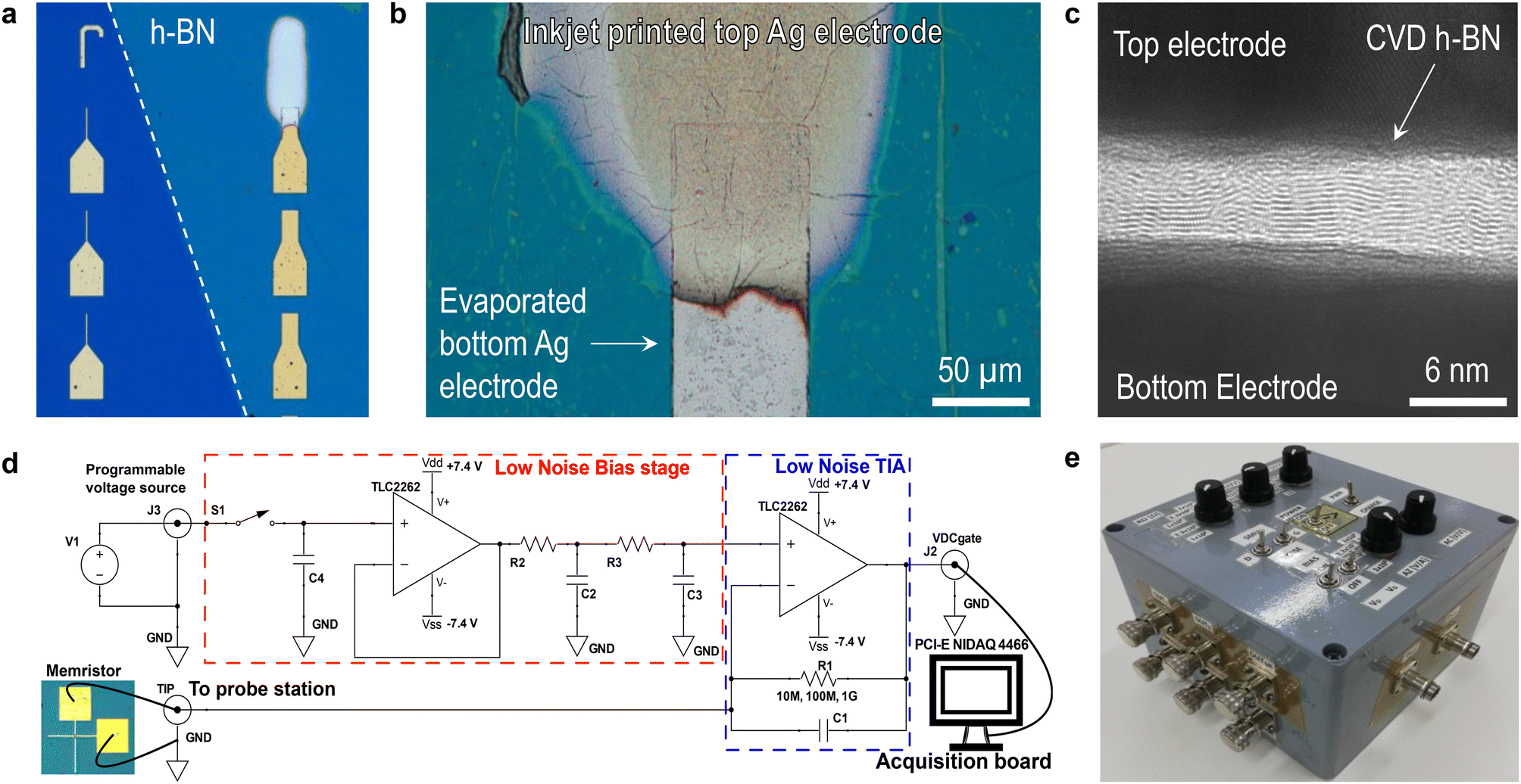 | ||
| Fig. 1 Device structure and custom low-noise instrumentation. (a and b) Optical microscopy images of the Ag/h-BN/Ag devices used in this study, in which the bottom Ag electrode has been deposited by photolithography, electron beam evaporation and lift-off, and the top Ag electrode has been patterned via inkjet-printing technology. The squared pads in (a) are 100 μm × 100 μm. (c) TEM image of the CVD-grown h-BN used in our devices. Note the layered structure with localized defective regions, characteristic of CVD-grown h-BN.43 Thickness of the h-BN stack is around 6 nm or ∼16 layers, consistent with the h-BN atomic layer thickness of ∼0.33 nm. (d) Schematics of the bias and conditioning circuit used to acquire low frequency noise and RTN signals in h-BN cross points using a probe station. (e) Photograph of the employed custom instrumentation (enclosed in a metal box) for flexible conditioning of noise signals. | ||
Pristine devices show low leakage currents (<1 pA) and a conductance increase of around 0.6 V during I–V sweeps, ascribed to the typical dielectric breakdown in h-BN based devices42 (see ESI Fig. 2†). Under this condition, when the Ag/h-BN/Ag devices are subjected to a low constant voltage stress (CVS) of only 70 mV, a highly stable two-level RTN current can be observed, as shown in Fig. 2a. The current stochastically fluctuates between the two levels (i.e., L1 ∼ 50 nA and L2 ∼ 90 nA), and the devices reach optimal functioning for >1 hour at 70 mV (see Fig. 2a–c and ESI Fig. 3†). These types of RTN current signals were previously observed in metal oxides, and they were attributed to charge trapping and de-trapping at atomic defects, normally an oxygen vacancy38 or an oxygen interstitial ion.39 In our devices, this behaviour is related to the presence of native defects within the volume of the h-BN stack, mainly lattice distortions formed during the CVD process at h-BN grain boundaries and on substrate imperfections, resulting in amorphous, boron vacancy-rich regions.41 This is supported by the fact that Au/h-BN/Au devices fabricated using mechanically exfoliated h-BN of the same thickness (which do not contain such CVD-related native defects) drive a much lower leakage current and do not exhibit RTN under CVS (see ESI Fig. 4 and 5†).
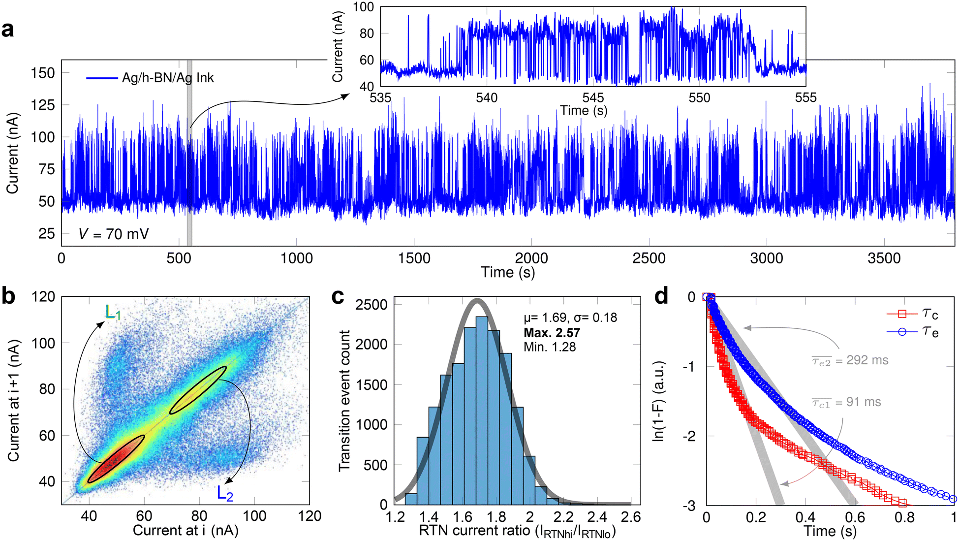 | ||
| Fig. 2 Tailoring RTN signals through electrode engineering. (a) RTN current through an Ag/h-BN/Ag-ink memristor device under a constant low applied voltage of 70 mV. The signal is stable for more than 1 hour, the longest ever reported for a 2D material-based device. The inset shows 20 seconds in detail, highlighting a large on/off ratio (larger than 2) and low capture and emission times for an RTN signal of unprecedented stability. (b) Weighted time lag plot of the RTN trace in panel (a). (c) Histogram showing the ratio of the currents before and after an RTN transition (calculated by dividing the high current over the low current, IRTNhi/IRTNlo). The curve is a Gaussian fit to the data with the mean μ = 1.69. The maximum value observed for a transition was 2.57. (d) Exponential plot of τc and τe distributions for the complete acquisition from panel (a). 87% of the transitions, i.e., ln(1 − F) > −2, taking place in less than 400 ms. Gray thick lines are visual aids of the mean values of bimodal exponential distributions. | ||
The plot in Fig. 2a is one of the longest RTN traces ever reported. Ref. 41 also reported RTN for >1 hour, but the device required 0.5 V to be operated and exhibited two current levels at ∼60 and ∼80 nA; that is, our Ag/h-BN/Ag device exhibits lower power consumption and a higher current on/off ratio (P = 5.25 nW and Ion/Ioff = 2 in Fig. 2aversus P = 35 nW and Ion/Ioff = 1.33 in ref. 41). Statistical analyses of the RTN signals were performed by creating a weighted scatter plot of the current data evaluated at the discrete time i + 1 vs. i (i.e., consecutive current values define y- and x-axes, respectively). This technique, called weighted time lag plot (w-TLP), has been often used as a characteristic figure-of-merit of RTN,44,45 allowing to clearly discriminate current levels even in noisy signals. The result shows two clear groups of data points, one for each current level of the RTN signal, as shown in Fig. 2b. Although useful for the qualitative assessment of long RTN acquisitions as in our case, this technique lacks information regarding the actual amplitude of each RTN transition. We extracted the ratio between the currents acquired immediately before and after each transition (calculated as IRTNhi/IRTNlo) from the trace in Fig. 2. We observed that these transitions have an average amplitude ratio of 1.69 and a maximum observed ratio of 2.57 (see Fig. 2c). These values are the highest among all the reported memristors used as the RTN source for TRNG circuits (see ESI Table 2†), which is an important advantage as it simplifies the design of the conditioning circuit required to harvest the entropy source.
We analysed the electron capture and emission times (τc and τe, respectively) at the native defects of the CVD-grown h-BN throughout the hidden Markov model (see ESI Fig. 6†).39 Our study reveals that τc and τe follow a bimodal distribution with mean values of τc1 = 79 ms and τc2 = 369 ms for capture times and slightly longer τe1 = 106 ms and τe2 = 437 ms for emission times (see Fig. 2d), much shorter than in ref. 46; this is also an advantage because, when used as a TRNG, it increases the speed for random bit generation. The superior RTN performance of the Ag/h-BN/Ag devices in Fig. 2 should be related to the use of a top inkjet-printed electrode; this deposition method, unlike electron beam evaporation and sputtering, does not damage the h-BN film during metal deposition. Fabrication induced defects can lead to strong instabilities and reduced reliability in h-BN devices.42 Thus, the origin of the RTN signal can be solely attributed to the intrinsic defects that are characteristic of CVD-grown multilayer h-BN, which are very highly localized.43 The low operating voltages of the devices, which are compatible with the complementary metal oxide semiconductor (CMOS) technology, should be related to the relatively large lateral size of the devices, which leads to the presence of larger clusters of defects (compared to smaller devices) that can be activated at lower voltages,48 as well as due to the high conductivity of Ag electrodes.
Some authors have suggested 2D material based devices as an entropy source for physically unclonable functions (PUF) due to their inherently high electrical variability after fabrication, which provides a device-unique fingerprint when challenged upon.47 Differently, due to their time-domain randomness, RTN signals produced by the Ag/h-BN/Ag memristors could be employed to implement TRNG circuits for advanced data encryption on-the-fly and one-time authentication factors.39,48 However, most studies characterizing RTN only demonstrate a few (<20) seconds of continuous functioning, the Ion/Ioff ratio is very small (<1.3), consume too much power, and the RTN only appears at one current range or is not consistent enough through time, which hinders the fabrication and commercialization of reliable RTN-enabled products. Here, we boost the performance of h-BN based memristors for cryptography by device engineering.
We presented a high-performance and inexpensive solution for the hardware implementation of a TRNG circuit by connecting an h-BN memristor to a commercial (Arduino) microcontroller board programmed in C language using the standard integrated design environment software provided by the manufacturer. In this implementation, the user sets a constant voltage to be applied to the h-BN memristor, which is generated by the Arduino board through a pulse-width-modulation (PWM) output (D5). As shown by the circuit schematics in Fig. 3a, the RTN current signal generated by the biased memristor is converted to voltage using a transimpedance amplifier, whose output is fed to one of the analogue inputs of the microcontroller (A1). This signal is periodically sampled (at 15 Hz) to generate a random seed for a 19-bit non-linear feedback register (NLFSR), which can be coded in the Arduino. If the current driven by the memristor reaches the current limitation by the TIA, this is interpreted as a conductance change in the memristor to a condition that is not optimum for TRNG operation. In such an event, the microcontroller switches the bias off, aided by a discharge transistor operated by a digital output (D11) of the microcontroller, and then applies the bias again, restoring the previous conductance of the device. During this interval, the TRNG continues to generate random numbers relying on the continuous operation of the NLFSR. This solution not only prevents the degradation of the memristive device by interrupting the bias, but also allows the TRNG to continue operating (i.e., producing a high-throughput random output) even if the RTN signal is interrupted for relatively long times up to 20 s (for a 19-bit NLFSR running at 30 Kbps, which can be enhanced including more bits in the register or temporarily reducing the bit generation rate). The seed will be 1 or 0 based on the measured current being above or below a defined threshold (respectively), which is typically at the middle of L1 and L2 although this value can be modified on the fly to prevent undesired drift—which, as shown in Fig. 2a, is not a problem in our devices. In the case of a large temporal drift, the output of the amplifier can be AC-coupled at the cost of an additional filter, and the edges of the RTN signal can be captured instead (no voltage reference required), without altering the results.34 A sketch of the physical implementation is shown in Fig. 3b, where the h-BN memristor is connected to the amplifier board (enclosed in the box shown in Fig. 1e), which is wired to the Arduino mounted on the protoboard. To confirm the correct functioning of the TRNG circuit, we connected a computer running a Python script that provides a live plot of the RTN current signal (see ESI Video 1†).
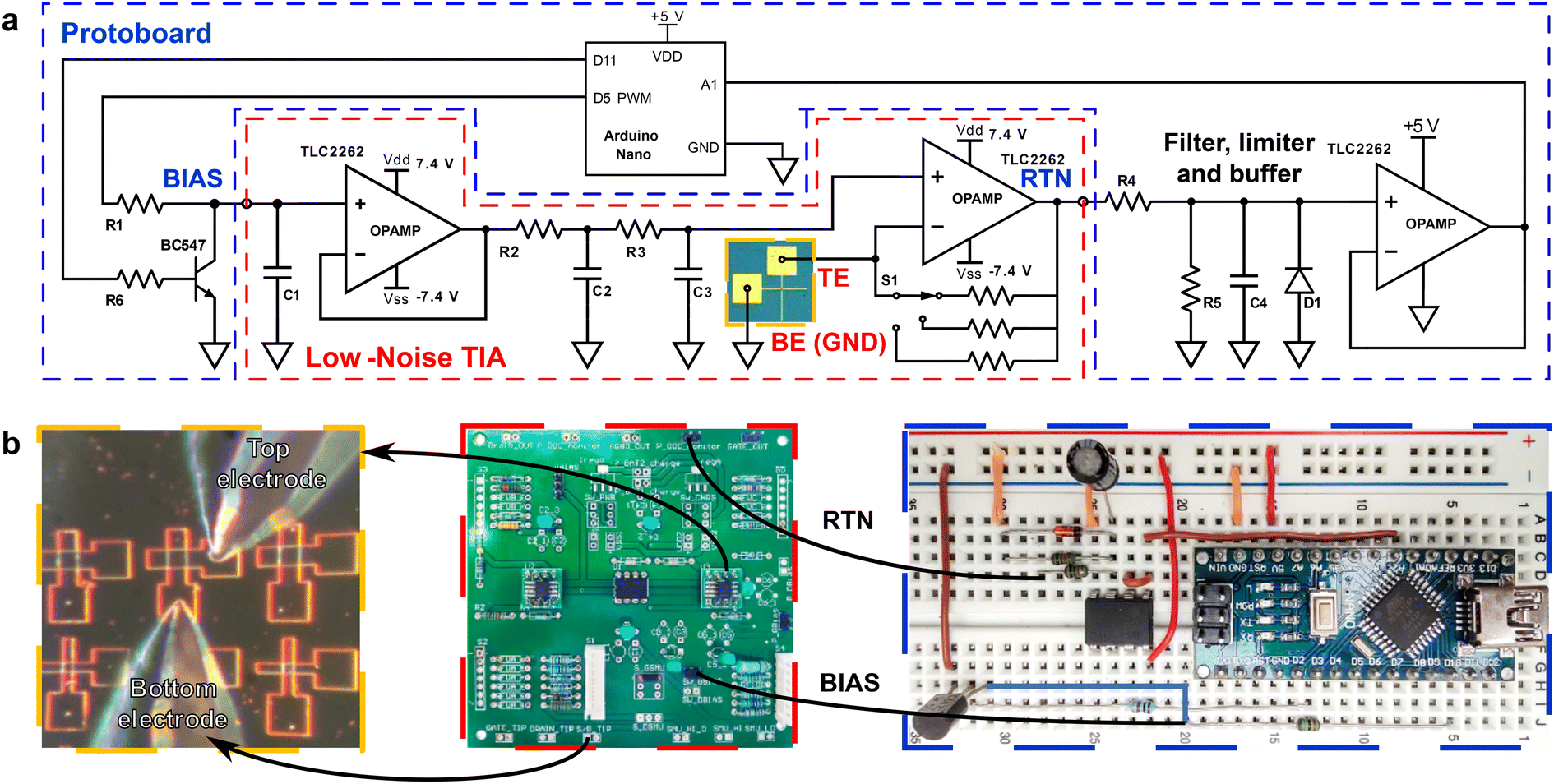 | ||
| Fig. 3 2D material enabled RTN-TRNG implementation. (a) Simplified schematics of the required circuitry to capture the entropy of an h-BN memristor. The low noise TIA is identical to the one used in the RTN experiments and is connected to an Arduino board together with signal conditioning circuitry. (b) Representation of the system implementation, where the h-BN memristor is connected via the probe station to a transimpedance amplifier that receives the bias signal from the Arduino and sends the amplified RTN signal to the microcontroller to reseed the NLFSR (see also ESI Video 1†). | ||
To test true random number generation, we evaluated the randomness of the output bitstream after 10 full periods of the NLFSR (totalizing more than 5 megabits) for all the input RTN signals using the randomness test suite from the National Institute of Standards and Technology (NIST).49 The results confirm that all 15 tests pass for significance levels of p > 0.001 (see the column labelled as the “RTN signal” in Fig. 4a); this can also be qualitatively observed in the chessboard-like representation of the signal (Fig. 4b), which looks completely random and free of any pattern. Note that if the output of the NLFSR circuit is mapped without putting any stochastic signal at the input, the circuit produces a repetitive pattern, as it can be easily observed in the corresponding chessboard-like diagram (see Fig. 4c). To test the robustness of the proposed implementation, we also tested the behaviour of this TRNG circuit using input signals of different natures, i.e., not only highly stochastic RTN signals (like the one in Fig. 2a) but also other signals generated by the h-BN memristors, such signals with high densities of low-frequency noise (flicker) and spiking current signals due to volatile switching (see ESI Fig. 7†). We confirm that the output of the TRNG when such signals are input also passes the randomness tests from the NIST (see columns labelled as “RTN + flicker” and “RTN + volatile RS signal” in Fig. 4a).
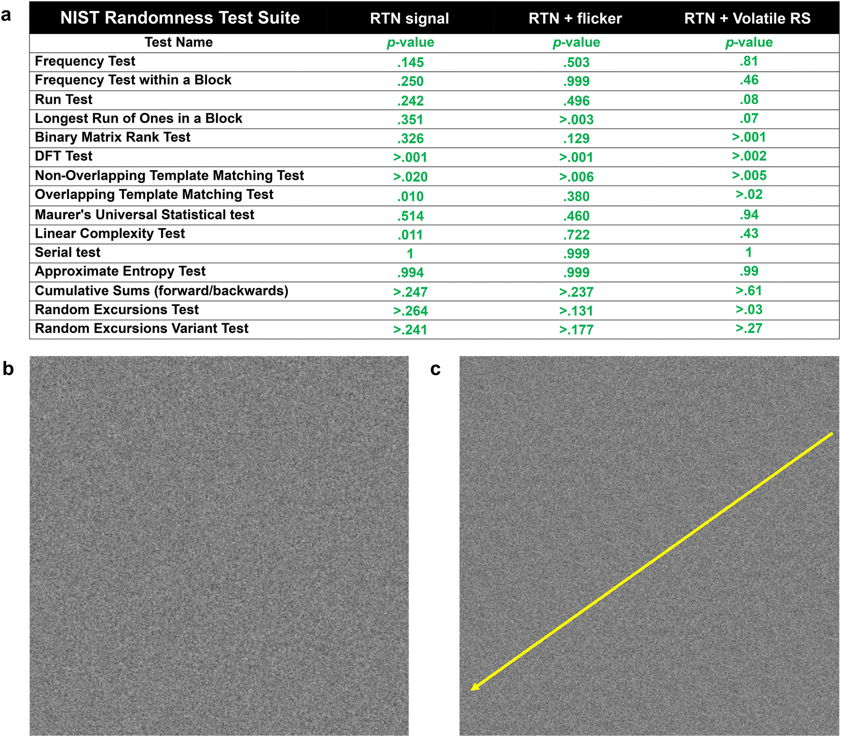 | ||
Fig. 4 Randomness tests, and TRNG and pseudo-RNG output bitmaps. (a) Results of the NIST randomness test suite expressed as a significance value of the statistical test p-value for three signals (produced by h-BN memristors) of different natures: showing stable RTN (similar to Fig. 2a) and showing complex low-frequency noise signals and spiking current signals due to volatile switching (similar to ESI Fig. 7†). All tests pass with a significance threshold p > 0.001 on a bitstream of 5![[thin space (1/6-em)]](https://www.rsc.org/images/entities/char_2009.gif) 242870 bits. (b) Visual chessboard-like representation of the output bitstream of the full TRNG implementation when using a stable RTN signal, after completing 10 full periods of the NLFSR, totalizing >5 megabits. These data are the same that are successfully put through the NIST tests in the third column of the table in panel (a). Note the absence of any distinguishable patterns on the bitmap. (c) The same visual chessboard-like representation but for the free-running 19-bit NLFSR (without any signal at the input) after completing 10 full periods. A clear repetitive pattern in the direction of the arrow is observed, included as a visual aid. 242870 bits. (b) Visual chessboard-like representation of the output bitstream of the full TRNG implementation when using a stable RTN signal, after completing 10 full periods of the NLFSR, totalizing >5 megabits. These data are the same that are successfully put through the NIST tests in the third column of the table in panel (a). Note the absence of any distinguishable patterns on the bitmap. (c) The same visual chessboard-like representation but for the free-running 19-bit NLFSR (without any signal at the input) after completing 10 full periods. A clear repetitive pattern in the direction of the arrow is observed, included as a visual aid. | ||
We selected this setup due to its low cost (≤20 $), small size (less than 2.5 cm × 7 cm × 1.5 cm) and low weight (<30 g), which allows integrating it in a very wide range of applications. This circuitry could also be fabricated on a silicon wafer featuring amplifiers, on-chip filters, active pseudo-resistors and a low noise DC-feedback loop, and it would occupy a total area of ∼0.024 mm2 (including passive components) if transistors of the 180 nm node are employed (see ESI Fig. 8†). Note that the cost of such area increase in a commercial multi-project wafer is ≤0.52 $ (see Methods). Furthermore, the h-BN device can be connected with the circuit using the same inkjet-printing technology used for the top electrode, as an inexpensive alternative to wire-bonding.50 On an embedded system, the TRNG block is expected to be a part of a larger IoT application; hence, it is relevant to report on the overhead power consumption of the entropy source and the external conditioning circuit, rather than that of the whole implementation. With this in mind, the power overhead is determined by the memristor (650 nW, see Fig. 2a) and the transimpedance amplifier (∼10 μW).51 This provides an average energy consumption of ∼3.3 nJ per bit when operating at 30 kilobit per s limited by the communication with the PC, which logs the results. This can be further improved to ∼1.28 pJ per bit when operating at a maximum throughput of ∼7.8 megabit per s (for the 19-bit NLFSR being reseeded at 15 Hz, i.e., 15 Hz × 219 bits) or even higher for the longer NLFSR by simply disconnecting the PC logging interface.
In conclusion, we have combined multilayer h-BN memristors with a commercially available microcontroller to provide a solution for highly reliable true random number generation for cryptographic systems. The key feature of our work is that the h-BN memristors exhibit highly stable RTN signals for long periods (>1 hour) and consume low power (∼650 nW), which are only observed when using top Ag electrodes deposited by inkjet-printing technology. We connected the h-BN memristors to a commercial microcontroller and developed the first highly reliable and low-power standalone hardware solution for TRNG generation enabled by these devices. It is important to emphasize that this TRNG architecture, while simple and inexpensive, has been demonstrated to be robust not only to the temporary interruption of the RTN signal but also to variations in the characteristics of the entropy source, such as the presence of dense background flicker noise or the random volatile switching of the device. These results represent a big step towards the fabrication of advanced TRNG circuits that are ideal for the internet-of-things, and also for the integration of 2D materials with classical electronics, exploiting the benefits of both platforms to achieve advanced performance.
Methods
CVD h-BN synthesis
The CVD-grown multilayer hexagonal boron nitride used in this study was directly obtained from Graphene Supermarket. h-BN was synthesized by chemical vapour deposition (CVD) on a 25 mm thick Cu foil at high temperatures of up to 900 °C using ammonia borane or borazine as a precursor. For further details on the synthesis process, the manufacturer refers to ref. 52. This process is well established and has been employed in multiple publications39,53–55 and is guaranteed by the manufacturer.Devices fabrication
The Ag/h-BN/Ag devices have been fabricated on a 300 nm SiO2/Si wafer from Rdmicro. The bottom electrodes of the devices consisted of 40 nm Ag, although we used a 10 nm Ti layer below it as an adhesion layer. The electrodes have been patterned by photolithography (mask aligner from SUSS), electron beam evaporation (PVD 75 from Kurt J. Lesker) and lift-off (in acetone for 12 hours). Ti and Ag were deposited at a low pressure of 2 × 10⁻⁵ Torr without breaking the vacuum. The shape of the electrodes consisted of a 100 μm × 100 μm squared pad with a 50 μm × 150 μm perpendicular wire connected to the centre of one of its sides. Then, the CVD-grown ∼18-layer-thick h-BN sheet was transferred on the bottom electrodes (see CVD h-BN transfer). Finally, Ag top electrodes have been patterned on the h-BN using a piezo-inkjet printer (DMP-2800, Fujifilm) with Ag ink (Jet 600C, Hisense). The area of the device was defined by the overlapping of a region between the patterned Ag line and the Ag bottom electrode below the h-BN, which was approximately 50 μm × 50 μm.CVD h-BN transfer
The wet transfer process employed in this study consists of seven steps. First, liquid poly(methyl methacrylate) (PMMA) was spin-coated on the h-BN/Cu sample at 500 rpm for 6 s and 3500 rpm for 30 s. Second, the PMMA/h-BN/Cu sample was heated at 100 °C for 3 min to improve its stability and adhesion to the h-BN/Cu sample. Third, the PMMA/h-BN/Cu sample was deposited on the surface of an iron chloride (FeCl3, 0.1 g ml−1) solution (i.e., floating) for 5 h to etch the Cu substrate. Fourth, the PMMA/h-BN sample was deposited on the surface of a hydrochloric acid (HCl, 2 wt%) solution (i.e., floating) for 30 min for cleaning. Fifth, further cleaning was conducted by depositing the PMMA/h-BN sample on the surface of deionized water (i.e., floating) for 1 h. Sixth, the PMMA/h-BN sample was obtained with the SiO2/Si wafer containing the Au/Ti bottom electrodes and heated at 60 °C for 5 min. Seventh, the sample was introduced in a glass with acetone (≥99%) for 12 h to etch PMMA.Exfoliated h-BN devices
The Au/h-BN/Au devices with mechanically exfoliated h-BN were fabricated using Scotch tape from 3M and bulk crystal h-BN powder from HQ Graphene Company. The transfer of the exfoliated h-BN from the Scotch tape to the Au bottom electrodes (patterned on the SiO2/Si sample) was carried out in a transfer stage from Shanghai Onway (model OWTS-01).Physical characterization
The images of the devices were collected using a DM400 optical microscope from Leica Microsystems and a Supra 55 scanning electron microscope from Zeiss. The cross-sectional characterization of the devices was carried out using a JEM-2100 transmission electron microscope from JEOL. TEM images were obtained by cutting the real Au/h-BN/Au devices into 40 nm-thick lamellas using a Helios NanoLab 450S focused ion beam from FEI. Many studies have shown that TEM characterization was performed right after material growth; however, this may ignore the defects introduced in the h-BN sheet during the electron beam evaporation process.51 In our case, the collection of TEM images after the fabrication of the device ensures that we are visualizing the real structure of the devices.Device characterization
Low voltage I–V and CVS I–t characteristics were measured using a Keysight B1500A semiconductor parameter analyser for a low leakage current floor of 10 fA and a minimum sampling time of roughly 10 ms. Current limitation was maintained below 10 μA in all SPA measurements. I–t data series were processed via MATLAB scripts for the computation of current histograms, weighted time lag plots (w-TLP).44,45 To perform low noise acquisitions of the RTN signals for the TRNG, a self-biased low noise TIA with a low noise bias source was implemented using off-the-shelf components, following the guidelines from the literature.52 The simplified circuit schematic is shown in Fig. 1d. Similar implementations have been used in the past to study the low frequency noise in nanoelectronic devices.56,57 The TIA bandwidth is ∼100 Hz at the highest selected gain and ∼10 kHz at the lowest gain. The low noise bias stage provides a stable voltage reference disconnected from external sources with sufficiently low DC drift for typical noise acquisitions lasting from a few to tens of minutes. The full circuit is battery powered and enclosed in a metal case to reduce the external interference, as shown in Fig. 1e. The amplifier includes an additional, configurable gain (2 to 101), AC-coupled, and voltage post-amplifier (see the board picture in Fig. 3b) stage to acquire the sharp edges of RTN signals decoupled from slow DC drifts that can alter the interpretation of the results. For the implementation of a TRNG, the general architecture is plausible of integration with a microcontroller (see the Arduino-based TRNG) and CMOS technology (see the circuit in ESI Fig. 7†).Arduino-based TRNG
In this solution, the Arduino generates the adequate bias for the device using a PWM output (D11) and a low pass filter R1–C1 (15 kΩ–10 μF). C1 was integrated with the custom TIA used for the experiments in previous sections, setting a low-noise DC bias for the DUT through the self-biased TIA. The output of the amplifier was then fed to a voltage limiter circuit R4–R5–D1 (R4 = R5 = 10 kΩ and D1 = 1N4148) to adapt the voltage range of −7.4 V–+7.4 V to a single, buffered 0-to-5 V max. output to make it compatible with the Arduino analogue input (A1), which samples the amplified current flowing through the memristor. C4 (22 μF) is included as an antialiasing filter for the input of the analogue-to-digital converter on the Arduino board. A resistor R6 (>1 K) connects a digital output (D11) to the base of a bipolar NPN transistor (BC547) that is saturated when the microcontroller detects a conductance state change (TIA saturation), aiding in the quick discharge of the PWM filter (which would alternatively discharge slowly through R1) and reducing the bias voltage of the device to 0 V in negligible time. A Python script runs in the PC and manages the execution of the TRNG experiment with a simple graphical interface to easily monitor the experiment from the PC and save all the results. Another independent thread from the Python code runs a live plot of the TIA output, monitoring the status of the device throughout the experiment and logging every event through time, such as seed changes and device set–reset occurrences. The execution of the experiment can be stopped at any time via keyboard interrupts or be set for a fixed run length, in this case set to 10 full periods of the 19-bit NLFSR. The complete Python code is available in a public Git repository (https://github.com/smpazos/hBN_TRNG.git). The Arduino platform requires to be loaded with the Standard Firmata sketch previously.The overhead price in the 180 nm CMOS implementation of the TRNG was calculated as follows. A commercial multi-project wafer (MPW) offering a full-block fabrication at a low level production cost of around 22000 $ and involves a total of 40 silicon microchips of 25 mm2 each, totalizing a silicon area of 1000 mm2. This results in a cost of 22 $ per mm2 of processed wafer. Considering the approximate area overhead of the circuit being ∼0.024 mm2 (see ESI Fig. 8c†), the price for each instance renders ≤0.52 $, which can be drastically reduced on full scale manufacturing.
Data availability
The data that support the findings of this study are available from the corresponding author upon reasonable request.Author contributions
M. L. and S. P. designed the project. W. Z., Y. S., Y. Y. and K. Z. prepared the samples and performed all the physical characterization of the materials and devices. S. P., T. B., F. A., and G. W. measured the electrical characteristics of the devices. S. P. designed and built the instrumentation and coded the TRNG. S. P., T. Z. and F. M. P. prepared the TRNG circuit and performed randomness tests. S. P. and M. L. wrote the article. All the authors discussed the results and revised the manuscript.Conflicts of interest
There are no conflicts to declare.Acknowledgements
This work was supported by the Ministry of Science and Technology of China (grants no. 2019YFE0124200 and 2018YFE0100800), the National Natural Science Foundation of China (grants no. 61874075), the Collaborative Innovation Centre of Suzhou Nano Science and Technology, the Priority Academic Program Development of Jiangsu Higher Education Institutions, the 111 Project from the State Administration of Foreign Experts Affairs of China, and the Baseline funding program of the King Abdullah University of Science and Technology. The authors also acknowledge the funding from the following Argentinean institutions: Ministerio de Ciencia, Tecnología e Innovación (MINCyT) under contracts, PICT 2016/0579, PME 2015-0196 and PICTE 2018-0192; UTN-FRBA under projects CCUTIBA4764TC, MATUNBA4936, CCUTNBA5182, and CCUTNBA6615.References
- A. Petritz, et al., Imperceptible energy harvesting device and biomedical sensor based on ultraflexible ferroelectric transducers and organic diodes, Nat. Commun., 2021, 12, 1–14 CrossRef PubMed.
- T. Sanislav, G. D. Mois, S. Zeadally and S. C. Folea, Energy Harvesting Techniques for Internet of Things (IoT), IEEE Access, 2021, 9, 39530–39549 Search PubMed.
- M. Alioto, Trends in hardware security from basics to ASICs, IEEE Solid-State Circuits Mag., 2019, 11, 56–74 Search PubMed.
- C. S. Pétrie and J. Alvin Connelly, A noise-based ic random number generator for applications in Cryptography, IEEE Trans. Circuits Syst. I: Fundam. Theory Appl., 2000, 47, 615–621 CrossRef.
- D. Liu, Z. Liu, L. Li and X. Zou, A Low-Cost Low-Power Ring Oscillator-Based Truly Random Number Generator for Encryption on Smart Cards, IEEE Trans. Circuits Syst. II: Express Briefs, 2016, 63, 608–612 Search PubMed.
- S. K. Mathew, et al., μRNG: A 300-950 mV, 323 Gbps/W All-Digital Full-Entropy True Random Number Generator in 14 nm FinFET CMOS, IEEE J. Solid-State Circuits, 2016, 51, 1695–1704 Search PubMed.
- N. Nguyen, G. Kaddoum, F. Pareschi, R. Rovatti and G. Setti, A fully CMOS true random number generator based on hidden attractor hyperchaotic system, Nonlinear Dyn., 2020, 102, 2887–2904 CrossRef.
- S. Liang, W. Zheng, Y. Cao and X. Zhao, A 30 fJ b−1 current-biased inverter based ro TRNG with high temperature and supply voltage stabilities, Proceedings - IEEE International Symposium on Circuits and Systems, 2020-October, 2020.
- W. Kai, Y. Cao, C. H. Chang and X. Ji, High-speed true random number generator based on differential current starved ring oscillators with improved thermal stability, Proceedings - IEEE International Symposium on Circuits and Systems, 2019-May, 2019.
- D. Ielmini and R. Waser, Resistive switching: from fundamentals of nanoionic redox processes to memristive device applications, Wiley-VCH, 2016 Search PubMed.
- R. Carboni and D. Ielmini, Stochastic Memory Devices for Security and Computing, Adv. Electron. Mater., 2019, 5, 1900198 CrossRef.
- R. Carboni and D. Ielmini, Applications of Resistive Switching Memory as Hardware Security Primitive, in Springer Series in Advanced Microelectronics, Springer Verlag, 2020, vol. 63, pp. 93–131 Search PubMed.
- Y. Pang, B. Gao, B. Lin, H. Qian and H. Wu, Memristors for Hardware Security Applications, Adv. Electron. Mater., 2019, 5, 1800872 CrossRef.
- S. Sahay and M. Suri, Recent trends in 0hardware security exploiting hybrid CMOS-resistive memory circuits, Semicond. Sci. Technol., 2017, 32, 123001 CrossRef.
- Y. Wang, W. Wen, M. Hu and H. Li, A novel true random number generator design leveraging emerging memristor technology, Proceedings of the ACM Great Lakes Symposium on VLSI, GLSVLSI, 20–22-May-, 2015, pp. 271–276.
- S. Balatti, S. Ambrogio, Z. Wang and D. Ielmini, True random number generation by variability of resistive switching in oxide-based devices, IEEE J. Emerg. Sel. Top. Circuits Syst., 2015, 5, 214–221 Search PubMed.
- S. Balatti, et al., Physical unbiased generation of random numbers with coupled resistive switching devices, IEEE Trans. Electron Devices, 2016, 63, 2029–2035 Search PubMed.
- S. Sahay, M. Suri, A. Kumar and V. Parmar, Hybrid CMOS-OxRAM RNG circuits, 16th International Conference on Nanotechnology - IEEE NANO 2016, 2016, pp. 393–396, DOI:10.1109/NANO.2016.7751437.
- R. Govindaraj, S. Ghosh and S. Katkoori, CSRO-Based Reconfigurable True Random Number Generator Using RRAM, IEEE Trans. Very Large Scale Integr. VLSI Syst., 2018, 26, 2661–2670 Search PubMed.
- R. Gu, Y. Sun, Y. Wang, W. Wang and Q. Li, A rate-adjustable true random number generator based on the stochastic delay of a TiN/NbOx/Pt memristor, AIP Adv., 2021, 11, 125301 CrossRef CAS.
- B. Lin , et al., A high-performance and calibration-free true random number generator based on the resistance perturbation in RRAM Array, Technical Digest - International Electron Devices Meeting, IEDM 2020-December, 38.6.1–38.6.4, 2020.
- B. Lin , et al., A High-Speed and High-Reliability TRNG Based on Analog RRAM for IoT Security Application, Technical Digest - International Electron Devices Meeting, IEDM 2019-December, 2019.
- T. Zhang, et al., High-speed true random number generation based on paired memristors for security electronics, Nanotechnology, 2017, 28, 455202 CrossRef PubMed.
- H. Aziza, et al., True Random Number Generator Integration in a Resistive RAM Memory Array Using Input Current Limitation, IEEE Trans. Nanotechnol., 2020, 19, 214–222 CAS.
- K. S. Woo, et al., A True Random Number Generator Using Threshold-Switching-Based Memristors in an Efficient Circuit Design, Adv. Electron. Mater., 2019, 5, 1800543 CrossRef.
- K. S. Woo, et al., A Combination of a Volatile-Memristor-Based True Random-Number Generator and a Nonlinear-Feedback Shift Register for High-Speed Encryption, Adv. Electron. Mater., 2020, 6, 1901117 CrossRef CAS.
- K. S. Woo, et al., A High-Speed True Random Number Generator Based on a CuxTe1−x Diffusive Memristor, Adv. Intell. Syst., 2021, 3, 2100062 CrossRef.
- G. Kim, et al., Self-clocking fast and variation tolerant true random number generator based on a stochastic mott memristor, Nat. Commun., 2021, 12, 1–8 CrossRef PubMed.
- B. Yang, et al., RRAM Random Number Generator Based on Train of Pulses, Electronics, 2021, 10, 1831 CrossRef CAS.
- H. Jiang, et al., A novel true random number generator based on a stochastic diffusive memristor, Nat. Commun., 2017, 8, 1–9 CrossRef CAS PubMed.
- G. Kim, et al., Self-clocking fast and variation tolerant true random number generator based on a stochastic mott memristor, Nat. Commun., 2021, 12, 1–8 CrossRef PubMed.
- C. Y. Huang, W. C. Shen, Y. H. Tseng, Y. C. King and C. J. Lin, A contact-resistive random-access-memory-based true random number generator, IEEE Electron Device Lett., 2012, 33, 1108–1110 Search PubMed.
- Z. Wei, et al., True random number generator using current difference based on a fractional stochastic model in 40-nm embedded ReRAM, Technical Digest - International Electron Devices Meeting, IEDM 4.8.1–4.8.4, 2017, DOI:10.1109/IEDM.2016.7838349.
- J. Yang, et al., A low cost and high reliability true random number generator based on resistive random access memory, Proceedings - 2015 IEEE 11th International Conference on ASIC, ASICON 2015, 2016. DOI:10.1109/ASICON.2015.7516996.
- N. Vasileiadis, P. Dimitrakis, V. Ntinas and G. C. Sirakoulis, True random number generator based on multi-state silicon nitride memristor entropy sources combination, 2021 International Conference on Electronics, Information, and Communication, ICEIC 2021, 2021, DOI:10.1109/ICEIC51217.2021.9369817.
- B. Gao, et al., A Unified PUF and TRNG Design Based on 40 nm RRAM with High Entropy and Robustness for IoT Security, IEEE Trans. Electron Devices, 2022, 69, 536–542 CAS.
- P. S. Yeh, et al., Self-Convergent Trimming SRAM True Random Number Generation with In-Cell Storage, IEEE J. Solid-State Circuits, 2019, 54, 2614–2621 Search PubMed.
- P. H. Tseng, et al., ReRAM-Based Pseudo-True Random Number Generator with High Throughput and Unpredictability Characteristics, IEEE Trans. Electron Devices, 2021, 68, 1593–1597 Search PubMed.
- C. Wen, et al., Advanced Data Encryption using 2D Materials, Adv. Mater., 2021, 33, 2100185 CrossRef CAS PubMed.
- F. Palumbo, et al., A Review on Dielectric Breakdown in Thin Dielectrics: Silicon Dioxide, High– k, and Layered Dielectrics, Adv. Funct. Mater., 2019, 30, 1900657 CrossRef.
- A. Oberoi, A. Dodda, H. Liu, M. Terrones and S. Das, Secure Electronics Enabled by Atomically Thin and Photosensitive Two-Dimensional Memtransistors, ACS Nano, 2021, 15(12), 19815–19827 CrossRef CAS PubMed.
- W. Zheng, et al., Defect-Free Metal Deposition on 2D Materials via Inkjet Printing Technology, Adv. Mater., 2021, 2104138, DOI:10.1002/ADMA.202104138.
- Y. Shen, et al., Variability and Yield in h-BN-Based Memristive Circuits: The Role of Each Type of Defect, Adv. Mater., 2021, 33, 2103656 CrossRef CAS PubMed.
- F. M. Puglisi, Noise in Resistive Random Access Memory Devices, in Noise in Nanoscale Semiconductor Devices, ed. T. Grasser, Springer, Cham, 2020, pp. 87–133. DOI:10.1007/978-3-030-37500-3_3.
- M. Maestro, et al., New high resolution Random Telegraph Noise (RTN) characterization method for resistive RAM, Solid-State Electron., 2016, 115, 140–145 CrossRef CAS.
- G. González-Cordero, M. B. González, F. Jiménez-Molinos, F. Campabadal and J. B. Roldán, New method to analyze random telegraph signals in resistive random access memories, J. Vac. Sci. Technol., B: Nanotechnol. Microelectron.: Mater., Process., Meas., Phenom., 2019, 37, 012203 Search PubMed.
- B. Shao, et al., Crypto primitive of MOCVD MoS2 transistors for highly secured physical unclonable functions, Nano Res., 2020, 14(6), 1784–1788 CrossRef.
- X. Li, et al., Random Telegraph Noise in Metal-Oxide Memristors for True Random Number Generators: A Materials Study, Adv. Funct. Mater., 2021, 31, 2102172 CrossRef CAS.
- L. Bassham, et al., A Statistical Test Suite for Random and Pseudorandom Number Generators for Cryptographic Applications, Preprint at https://tsapps.nist.gov/publication/get_pdf.cfm?pub_id=906762, 2010.
- Y. Liu, et al., Inkjet Printing: A Cheap and Easy-to-Use Alternative to Wire Bonding for Academics, Cryst. Res. Technol., 2022, 57, 2100210 CrossRef CAS.
- LMP2231 data sheet, product information and support | TI.com. https://www.ti.com/product/LMP2231.
- K. K. Kim, et al., Synthesis and characterization of hexagonal boron nitride film as a dielectric layer for graphene devices, ACS Nano, 2012, 6, 8583–8590 CrossRef CAS PubMed.
- S. Chen, et al., Wafer-scale integration of two-dimensional materials in high-density memristive crossbar arrays for artificial neural networks, Nat. Electron., 2020, 3, 638–645 CrossRef CAS.
- Y. Shi, et al., Electronic synapses made of layered two-dimensional materials, Nat. Electron., 2018, 1, 458–465 CrossRef.
- K. Y. Ma, M. Kim and H. S. Shin, Large-Area Hexagonal Boron Nitride Layers by Chemical Vapor Deposition: Growth and Applications for Substrates, Encapsulation, and Membranes, Acc. Mater. Res., 2022, 3, 748–760 CrossRef CAS.
- G. Giusi, F. Crupi, C. Ciofi, C. Pace and P. Magnone, Instrumentation design for cross-correlation measurements between gate and drain low frequency noise in MOSFETs, Fluctuation Noise Lett., 2010, 9, 313–322 CrossRef.
- P. Magnone, et al., $1/f$ Noise in Drain and Gate Current of MOSFETs With High-$k$ Gate Stacks, IEEE Trans. Device Mater. Reliab., 2009, 9, 180–189 CAS.
Footnote |
| † Electronic supplementary information (ESI) available: Eight additional figures, two tables and one video, as well as details of the design, fabrication, measurement and modelling protocols. See DOI: https://doi.org/10.1039/d2nr06222d |
| This journal is © The Royal Society of Chemistry 2023 |