
Interfacial thermal conductance between atomically thin boron nitride and graphene
Qiuhui V.
Yu
 a,
Kenji
Watanabe
b,
Takashi
Taniguchi
b and
Lu Hua
Li
*a
a,
Kenji
Watanabe
b,
Takashi
Taniguchi
b and
Lu Hua
Li
*a
aInstitute for Frontier Materials, Deakin University, Waurn Ponds, Victoria 3216, Australia. E-mail: luhua.li@deakin.edu.au
bNational Institute for Materials Science, Namiki 1-1, Tsukuba, Ibaraki 305-0044, Japan
First published on 7th December 2022
Abstract
Atomically thin hexagonal boron nitride (BN) is a promising dielectric substrate for graphene and other two-dimensional (2D) materials for performance enhancement and heat dissipation. However, the interfacial heat conductance between atomically thin BN and graphene has not been experimentally studied yet. Here, we report that the interfacial thermal conductance between high-quality graphene and trilayer BN is 9.64 ± 2.12 MW m−2 K−1 in the temperature range of 293–393 K, indicating that the interfacial thermal conductance is depressed when the heterostructure thickness is smaller than the wavelength of the low-frequency phonons, e.g. ZA in BN.
Introduction
Thermal management in nano-devices is a great challenge. Inadequate waste heat dissipation, especially at the “hot spots” (i.e. heat localized regions) degrades the performance, functionality, stability, efficiency, and safety of emerging transistors, light-emitting diodes (LEDs), and bio-sensors based on the heterostructures of two-dimensional (2D) materials, such as graphene and monolayer (1L) transition metal dichalcogenides (TMDs).1–3 For example, hot spots due to Joule heating have been observed in graphene-based field effect transistors (FETs), causing device failure at 1 mW μm−2 when the local temperature reached ∼400 °C;4 graphene-based bio-implants and bio-sensors heat up and ultimately kill the surrounding cells during operation.5 In spite of graphene's high thermal conductivity, the in-plane heat dissipation in a one-atom-thin material is negligible when the lateral size of the 2D device is larger than submicrometers. Significant overpopulation of phonons can be induced by electron flow, impeding heat transport at high currents in graphene owing to strong electron–phonon scattering. Furthermore, inevitable defects, wrinkles and strain in 2D materials can lead to hot spots. Overheating problems are even more severe in other 2D materials, such as atomically thin transition metal dichalcogenides (TMDs). For example, the breakdown power for 1L tungsten diselenide (WSe2) on silicon oxide (SiO2) was <0.01 mW μm−2.6 Therefore, efficient cooling is important for the practical use of atomically thin devices.Atomically thin hexagonal boron nitride (BN) is a promising dielectric substrate for 2D heterostructures because of its wide bandgap of 5.9 eV, absence of charges and dangling bonds, atomic smoothness, extraordinary mechanical properties, and excellent in-plane thermal conductivity.7–9 It has been reported that atomically thin BN could greatly enhance the mobility of graphene and WSe2 field-effect transistors (FETs).10–12 In addition, atomically thin BN could provide effective heat dissipation of the 2D heterostructure devices. Choi et al. experimentally proved that the temperature of a localized hot spot in graphene based FETs drops dramatically when hBN rather than SiO2/Si is employed as a heat spreader.13 Moreover, Liu et al. demonstrated that 2D BN could bridge the vibrational spectrum and enhance interfacial heat conductance in WSe2 based FETs.6
Therefore, it is important to understand the interfacial thermal conductance between atomically thin BN and other 2D materials. High interfacial thermal conductance has been predicted between graphene and BN heterostructure because of the highly matched phonon density of states (PDOS).14 However, it was theoretically demonstrated that the interfacial heat conductance between graphene and BN decreased with the layer reduction of BN.15 This phenomenon was ascribed to the contribution from the low-frequency phonons with long mean free path, similar to the thickness effect on the out-of-plane thermal conductivity of 2D materials.16 The experimental study of the interfacial thermal conductance between graphene and atomically thin (i.e. mono- and few-layer) BN is still lacking, though there have been several experimental results on that between graphene and bulk BN.13,14,17,18 Part of these experiments were based on the optothermal Raman technique; others on Joule heating method combing with the Raman technique.19 Heat conduction in graphene is dominated by acoustic and optical phonons due to the strong covalent sp2 bonding.20 Optothermal Raman technique have been widely used for in-plane thermal conductivity measurement of graphene or other 2D materials. However, the uncertainty of this technique was reported to be up to 40% in the absolute thermal conductivity value.21
In this study, we experimentally measured the interfacial thermal conductance between graphene and few-layer BN for the first time. The measurements were based on Joule heating of the heterostructure devices without the effect of in-plane heat spreading using Raman spectroscopy. In our experiment and calculation, we assumed that the heat distributed evenly and uniformly over both graphene and BN layers, and the small heat loss to the ambient and the heat induced by Raman laser were neglected.
Experimental
Fig. 1(a) displays the optical image of a graphene/atomically thin BN heterostructure device. The graphene and BN were mechanically exfoliated from highly oriented pyrolytic graphite (HOPG) and a single crystal hBN on SiO2(90 nm)/Si substrates, respectively. The transfer was assisted by the polymer stack of polydimethylsiloxane (PDMS) and polymethyl methacrylate (PMMA), followed by acetone and glacial acetic acid cleaning. It was reported that glacial acetic acid was effective to remove PMMA residue on 2D materials.22 Photolithography and reactive ion etching (RIE) were then used to cut the heterostructure to a 15 × 5 μm rectangular area for more accurate measurements on interfacial thermal conductance. After another round of photolithography and E-beam evaporation, Cr/Au (5 nm/50 nm) electrodes were deposited on the graphene/BN heterostructures, as shown in Fig. 1(a). Four electrodes were deposited: the outer electrodes were used for Joule heating; while the inner electrodes were for precise voltage measurement without the influence of contact resistance between the electrodes and heterostructures. The heterostructure between the two large electrodes was 10 × 5 μm. The devices were annealed at 400 °C in vacuum for better interface contact and less strain during Joule heating.23,24 Two devices were made. In the Raman calibrations of graphene and atomically thin BN as a function of temperature, a temperature-controlled stage was used. Next, a series of current was applied to the exfoliated graphene to electrically heat it. Due to the high-quality of the graphene mechanically exfoliated from highly oriented pyrolytic graphite (HOPG), we assumed that the current and heat distributed uniformly over it.25 The actual voltage and current were in the range of 0–26.5 V and 0–0.46 mA, respectively. The temperatures of the graphene and atomically thin BN were measured by micro-Raman, where the interfacial thermal conductance could be calculated. The Raman spectra were collected using a Renishaw inVia micro-Raman system equipped with a 514.5 nm laser and a 50× objective lens with a numerical aperture of 0.75. Also, the laser power was relatively small to minimize the heating effect. Fig. 1(b) shows the schematic of the four-probe measurement. The Joule heating method was chosen due to its more accuracy than optical heating which suffers from high uncertainties in light absorption of atomically thin materials and heat loss to the ambient.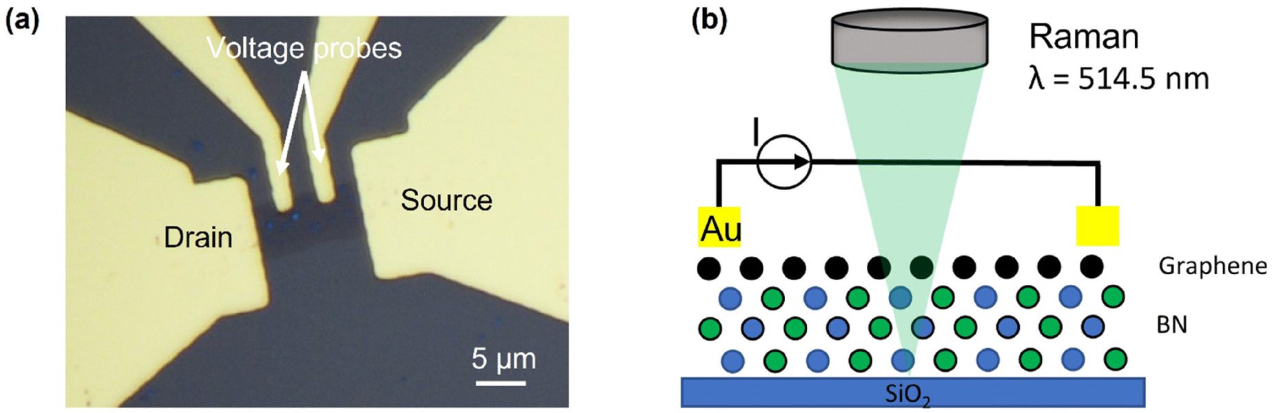 | ||
| Fig. 1 (a) Optical image of a graphene/atomically thin BN heterostructure device; (b) cross-sectional schematic of the device structure with four-probe configuration. | ||
Results and discussion
The temperature coefficient of the graphene and BN at 293–393 K was measured by Raman spectroscopy.26,27Fig. 2(a) shows the Raman spectra of the heterostructure. The stronger 2D band than the G band confirmed that the graphene was monolayer. The Raman intensity of the BN was much lower due to the far off-resonance excitation28 and its atomically thin nature.29 As expected, the Raman frequencies of both graphene and 3L BN downshifted with increased temperature, as shown in Fig. 2(b). The temperature dependence of the Raman frequency of graphene and atomically thin BN can be described by:7,27,30,31| ω = ω0 + χT | (1) |
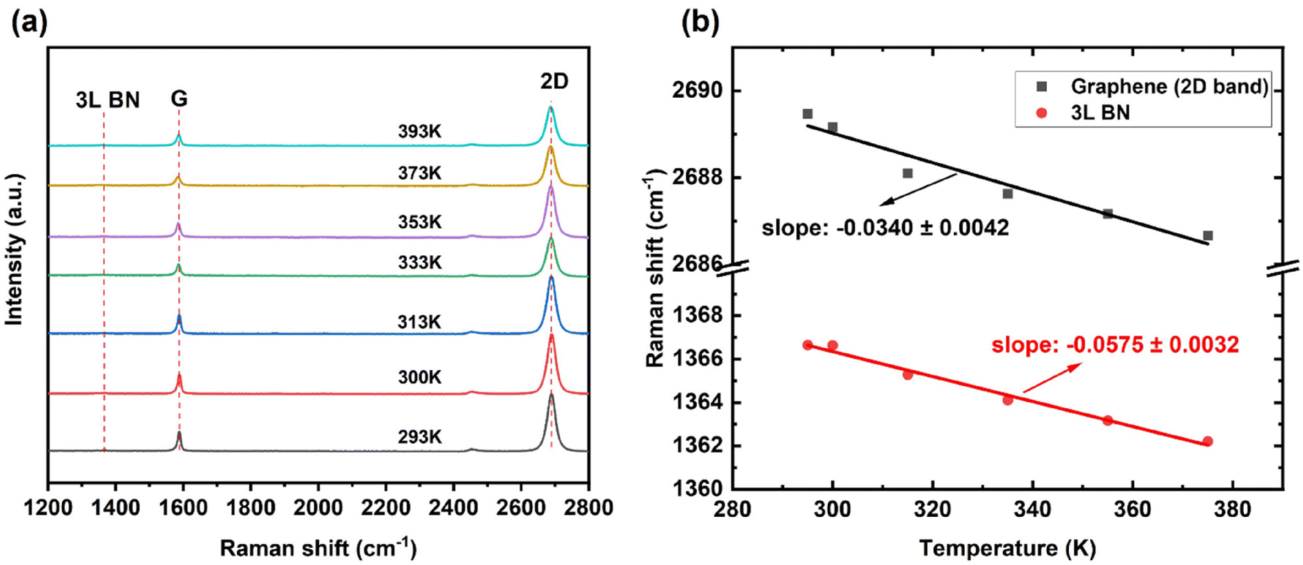 | ||
| Fig. 2 (a) Raman spectra and (b) the corresponding first-order temperature coefficients of the graphene and BN as a function of temperature. | ||
Fig. 3(a) show the Raman spectra of the graphene/BN heterostructure under different Joule heating power. As shown in Fig. 3(b), the Raman bands of both graphene and BN redshifted with increased electrical power, indicating effective Joule heating of the graphene. Also, both the G and 2D bands of the graphene showed no difference before and after the Joule heating, suggesting the lack of electrostatic doping. The Joule heating induced Raman frequency downshifts had coefficients of −0.2077 ± 0.0174 cm−1 mW−1 for graphene (2D band) and −0.2110 ± 0.0271 cm−1 mW−1 for BN, respectively. The temperature of the graphene and BN as the function of Joule heating power could be calculated by eqn (1).
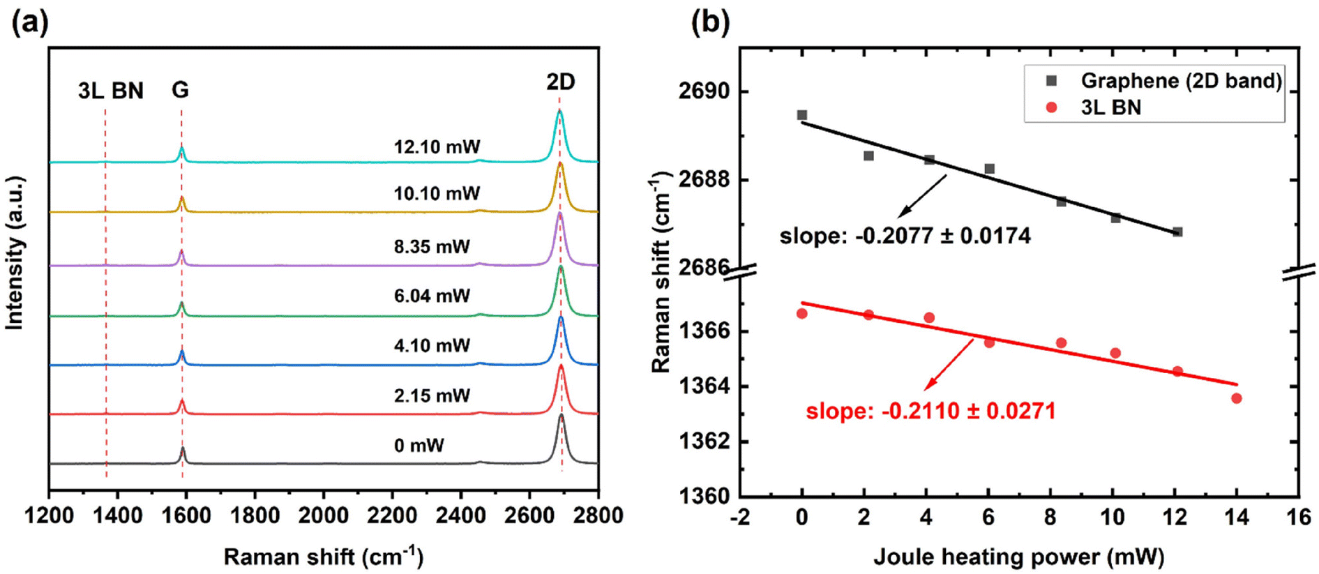 | ||
| Fig. 3 (a) Raman spectra and (b) Raman frequency shifts of the graphene and BN as a function of Joule heating power. | ||
The interfacial thermal conductance (G) between graphene and BN was calculated by:
| G = P/(A × ΔT) | (2) |
| ΔT = TGr − TBN = P[(χp/χT)Gr − (χp/χT)BN] | (3) |
Many factors could affect the interfacial thermal conductance, such as surface roughness, bubbles formed during heterostructure preparation, interface cleanness, and lattice mismatch, all of which were inevitable despite of careful sample preparation and measuring procedures. For example, acetic acid was used for better interface cleanness; vacuum heating could reduce lattice mismatch and strain during Joule heating; the Joule heating method avoided the in-plane heat spreading in the optical heating method. Our close-to two orders of magnitude difference between the experimental measurement and theoretical calculation was in line with the previous reports on other 2D heterostructures.33 Nevertheless, our results suggest smaller interfacial heat conductance between atomically thin BN and graphene than that between bulk hBN and graphene. The low-frequency ZA phonons dominate the out-of-plane heat conduction in 2D materials and their heterostructures.27 When the thickness of a heterostructure is smaller than the wavelength of ZA phonons as in our case, the contribution to the interfacial thermal conductance by these phonons is eliminated.16
Conclusions
We experimentally measured the interfacial thermal conductance between atomically thin BN and graphene. Based on the Joule heating induced temperature change measured by the Raman shift, the interfacial thermal conductance of the atomically thin BN and graphene heterostructure was 9.64 ± 2.12 MW m−2 K−1 in the temperature range of 293–393 K. Our results suggested that the atomic thickness of 2D heterostructure could reduce the interfacial thermal conductance because the contribution of the low-frequency phonons was depressed.Author contributions
Qiuhui V. Yu: formal analysis, investigation, writing – original draft, writing – review & editing; Kenji Watanabe and Takashi Taniguchi: hBN single crystals; Lu Hua Li: conceptualization, investigation, writing – review & editing, project administration, supervision.Conflicts of interest
There are no conflicts to declare.Acknowledgements
This work was performed in part at the Melbourne Centre for Nanofabrication (MCN) in the Victorian Node of the Australian National Fabrication Facility (ANFF).References
- K. L. Grosse, M. H. Bae, F. F. Lian, E. Pop and W. P. King, Nat. Nanotechnol., 2011, 6, 287–290 CrossRef PubMed.
- M. H. Bae, Z. Y. Ong, D. Estrada and E. Pop, Nano Lett., 2010, 10, 4787–4793 CrossRef PubMed.
- H. Nakajima, T. Morimoto, Y. Okigawa, T. Yamada, Y. Ikuta, K. Kawahara, H. Ago and T. Okazaki, Sci. Adv., 2019, 5, eaau3407 CrossRef PubMed.
- T. E. Beechem, R. A. Shaffer, J. Nogan, T. Ohta, A. B. Hamilton, A. E. McDonald and S. W. Howell, Sci. Rep., 2016, 6, 26457 CrossRef PubMed.
- G. Reina, J. M. Gonzalez-Dominguez, A. Criado, E. Vazquez, A. Bianco and M. Prato, Chem. Soc. Rev., 2017, 46, 4400–4416 RSC.
- D. Liu, X. Chen, Y. Yan, Z. Zhang, Z. Jin, K. Yi, C. Zhang, Y. Zheng, Y. Wang, J. Yang, X. Xu, J. Chen, Y. Lu, D. Wei, A. T. S. Wee and D. Wei, Nat. Commun., 2019, 10, 1188 CrossRef PubMed.
- S. Tian, Y. Yang, Z. Liu, C. Wang, R. Pan, C. Gu and J. Li, Carbon, 2016, 104, 27–32 CrossRef.
- A. Falin, Q. Cai, E. J. G. Santos, D. Scullion, D. Qian, R. Zhang, Z. Yang, S. Huang, K. Watanabe, T. Taniguchi, M. R. Barnett, Y. Chen, R. S. Ruoff and L. H. Li, Nat. Commun., 2017, 8, 15815–15815 CrossRef PubMed.
- Q. Cai, D. Scullion, A. Falin, K. Watanabe, T. Taniguchi, Y. Chen, E. J. G. Santos and L. H. Li, Nanoscale, 2017, 9, 3059–3067 RSC.
- C. R. Dean, A. F. Young, I. Meric, C. Lee, L. Wang, S. Sorgenfrei, K. Watanabe, T. Taniguchi, P. Kim, K. L. Shepard and J. Hone, Nat. Nanotechnol., 2010, 5, 722–726 CrossRef PubMed.
- S.-H. Jo, D.-H. Kang, J. Shim, J. Jeon, M. H. Jeon, G. Yoo, J. Kim, J. Lee, G. Y. Yeom, S. Lee, H.-Y. Yu, C. Choi and J.-H. Park, Adv. Mater., 2016, 28, 4824–4831 CrossRef CAS.
- B. Liu, Y. Ma, A. Zhang, L. Chen, A. N. Abbas, Y. Liu, C. Shen, H. Wan and C. Zhou, ACS Nano, 2016, 10, 5153–5160 CrossRef.
- D. Choi, N. Poudel, S. Park, D. Akinwande, S. B. Cronin, K. Watanabe, T. Taniguchi, Z. Yao and L. Shi, ACS Appl. Mater. Interfaces, 2018, 10, 11101–11107 CrossRef PubMed.
- R. Mao, B. D. Kong, K. W. Kim, T. Jayasekera, A. Calzolari and M. Buongiorno Nardelli, Appl. Phys. Lett., 2012, 101, 113111 CrossRef.
- W. Ren, Y. Ouyang, P. Jiang, C. Yu, J. He and J. Chen, Nano Lett., 2021, 21, 2634–2641 CrossRef.
- W. Ouyang, H. Qin, M. Urbakh and O. Hod, Nano Lett., 2020, 20, 7513–7518 CrossRef PubMed.
- C.-C. Chen, Z. Li, L. Shi and S. B. Cronin, Appl. Phys. Lett., 2014, 104, 081908 CrossRef.
- Y. Liu, Z.-Y. Ong, J. Wu, Y. Zhao, K. Watanabe, T. Taniguchi, D. Chi, G. Zhang, J. T. L. Thong, C.-W. Qiu and K. Hippalgaonkar, Sci. Rep., 2017, 7, 43886 CrossRef PubMed.
- H. Malekpour and A. A. Balandin, J. Raman Spectrosc., 2018, 49, 106–120 CrossRef.
- A. A. Balandin, ACS Nano, 2020, 14, 5170–5178 CrossRef PubMed.
- A. A. Balandin, Nat. Mater., 2011, 10, 569–581 CrossRef.
- M. Her, R. Beams and L. Novotny, Phys. Lett. A, 2013, 377, 1455–1458 CrossRef.
- T. Uwanno, Y. Hattori, T. Taniguchi, K. Watanabe and K. Nagashio, 2D Mater., 2015, 2, 041002 CrossRef.
- J. Boddison-Chouinard, S. Scarfe, K. Watanabe, T. Taniguchi and A. Luican-Mayer, Appl. Phys. Lett., 2019, 115, 231603 CrossRef.
- L. Levitov and G. Falkovich, Nat. Phys., 2016, 12, 672–676 Search PubMed.
- I. Calizo, A. A. Balandin, W. Bao, F. Miao and C. N. Lau, Nano Lett., 2007, 7, 2645–2649 CrossRef.
- Q. Cai, D. Scullion, W. Gan, A. Falin, S. Zhang, K. Watanabe, T. Taniguchi, Y. Chen, E. J. G. Santos and L. H. Li, Sci. Adv., 2019, 5, eaav0129 CrossRef.
- J. Ling, X. Miao, Y. Sun, Y. Feng, L. Zhang, Z. Sun and M. Ji, ACS Nano, 2019, 13, 14033–14040 CrossRef PubMed.
- R. V. Gorbachev, I. Riaz, R. R. Nair, R. Jalil, L. Britnell, B. D. Belle, E. W. Hill, K. S. Novoselov, K. Watanabe, T. Taniguchi, A. K. Geim and P. Blake, Small, 2011, 7, 465–468 CrossRef.
- N. Hosoya, Y. Akaho, M. Inoue, S. Sahoo and M. Tachibana, Appl. Phys. Lett., 2014, 105, 023108 CrossRef.
- Q.-Y. Li, K. Xia, J. Zhang, Y. Zhang, Q. Li, K. Takahashi and X. Zhang, Nanoscale, 2017, 9, 10784–10793 RSC.
- E. T. Swartz and R. O. Pohl, Appl. Phys. Lett., 1987, 51, 2200–2202 CrossRef CAS.
- Y. Xiong, X. Yu, Y. Huang, J. Yang, L. Li, N. Yang and D. Xu, Mater. Today Phys., 2019, 11, 100139 CrossRef.
| This journal is © The Royal Society of Chemistry 2023 |