
 Open Access Article
 This Open Access Article is licensed under a
 Creative Commons Attribution 3.0 Unported Licence
A sprayed graphene transistor platform for rapid and low-cost chemical sensing†
Benji
Fenech-Salerno‡
 a,
Martin
Holicky‡
a,
Chengning
Yao
a,
Anthony E. G.
Cass
a and
Felice
Torrisi
*ab
a,
Martin
Holicky‡
a,
Chengning
Yao
a,
Anthony E. G.
Cass
a and
Felice
Torrisi
*ab
aImperial College London, Department of Chemistry, Molecular Sciences Research Hub, 82 Wood Lane, London W12 0BZ, UK. E-mail: f.torrisi@imperial.ac.uk
bDipartimento di Fisica e Astronomia, Universita’ di Catania & CNR-IMM (Catania Università), Via S. Sofia 64, 95123 Catania, Italy
First published on 24th January 2023
Abstract
We demonstrate a novel and versatile sensing platform, based on electrolyte-gated graphene field-effect transistors, for easy, low-cost and scalable production of chemical sensor test strips. The Lab-on-PCB platform is enabled by low-boiling, low-surface-tension sprayable graphene ink deposited on a substrate manufactured using a commercial printed circuit board process. We demonstrate the versatility of the platform by sensing pH and Na+ concentrations in an aqueous solution, achieving a sensitivity of 143 ± 4 μA per pH and 131 ± 5 μA per log10Na+, respectively, in line with state-of-the-art graphene chemical sensing performance.
1. Introduction
The rapid ever-growing need for improved chemical and biological sensing platforms has ushered in a race for diagnostic technologies.1,2 The applications span beyond health, and include environmental monitoring, agriculture, and food processing industry,3–6 requiring sensors to satisfy a range of criteria, such as being sensitive and selective to analytes within diagnostically-relevant ranges, in real-time, at a low-cost, and easy to operate by the end user.7Chemical sensors (also known as chemosensors) are a broad family of sensors which are used to extract information on the chemical composition of a sample.8 In particular, electrochemical sensors are among the largest and oldest class of chemical sensors, whereby the measurand is detected as a measurable current (amperometry or voltammetry), measurable potential (potentiometry) or measurable change in the conductive properties of a medium between electrodes (conductometry).9 All three sensor architectures have reached commercial maturity, with devices such as the amperometric glucose sensor,10 potentiometric ion sensors11 and conductometric vapour sensors.12
New materials enable a wide range of sensors to be created.13–17 Graphene, a single layer of carbon atoms arranged in a hexagonal lattice, has been successfully used in a wide variety of sensors ranging from simple ion detection, through gas sensing to highly specific and sensitive biomolecule recognition.18–20 Graphene has various highly attractive properties for sensing, including an extremely high surface to volume ratio yielding excellent sensitivity21 and easy functionalisation due to its carbon chemistry.22
A range of electrochemical sensors can be constructed using graphene – for instance potentiometric, where the voltage between graphene film and a reference electrode is measured and can be used for the determination of ions and organic molecules.23,24 Graphene chemiresistive sensors use the change in electrical resistance of graphene film to perform gas sensing.25 Graphene can also be used as the channel in a field-effect transistor (FETs) which allows for very sensitive and fast detection over tunable, diagnostically relevant ranges.26,27
A graphene FET (GFET) consists of a graphene film across the source and drain electrodes forming the FET channel with the gate electrode separated by either a dielectric (dielectric-gated GFET, DG-GFET) or an electrolyte (electrolyte-gated GFET, EG-GFET, also referred to as solution-gated GFET, SG-GFET or liquid-gated GFET, LG-GFET).27 In both cases, a potential applied at the gate electrode can modulate the current flowing through the graphene channel due to the field effect.27 In the case of EG-GFETs, the actual gate voltage seen by the channel is affected by the double layer capacitance, graphene quantum capacitance and electrochemical potentials which enable the sensing of various analytes.28–31
The selectivity of GFET sensors is enabled by the functionalisation of the channel or the gate with a receptor molecule responding to a particular analyte. The breadth of receptor structures used is extensive and includes enzymes,32 aptamers,33 antibodies,34 peptide nucleic acids,35 single-strand deoxyribonucleic acid (ssDNA)36 and ion-selective membranes (ISMs).37
The graphene channel in EG-GFET sensors is typically achieved by chemical vapour deposition (CVD) of graphene on a copper foil and subsequent transfer of the graphene onto the desired substrate.38,39 However, a simpler and scalable approach is available through solution-processable graphene inks which are prepared by liquid-phase exfoliation (LPE) through sonication,40–42 hear mixing43 or microfluidisation44 of graphite. The resulting inks can be then deposited by spray-coating,45 ink-jet printing,46 screen-printing47 or aerosol-jet printing.48 This forms thin films consisting of a network of single-layer graphene (SLG) and few-layer graphene (FLG) flakes with average flake thickness varying from 2 to 10 nm (ref. 44, 49 and 50) and carrier mobility of up to 150 cm2 V−1 s−1.49 However, unlike CVD graphene, LPE graphene has only seen limited use in EG-GFET sensors51 despite its obvious advantages in terms of ink production scalability and the ease of its deposition.52
Rapid prototyping and scalable manufacturing of commercial chemical sensing test strips requires the sensors to be accurate and precise.53 These factors are strongly influenced by the device substrate and electrode design.54 For EG-FETs, the electrodes need to be electrochemically inert, typically made from gold.27 The geometry of the channel and the ratio of its width (W) to length (L) impact the overall channel resistance and the signal to noise ratio.54 Shorter channel length or longer channel width at a constant channel area result in higher currents at a given drain-source voltage (VDS)54 which then enables clear separation between the currents flowing through the graphene that are relevant to sensing and any leakage currents flowing through the electrolyte. A commercial printed circuit board (PCB) manufacturing process can provide repeatable and well-defined electrodes with sufficiently high resolution (<100 μm) enabling the manufacture of short and wide-channel electrodes, at an industrial scale.55
In this work, we present a novel route to manufacture EG-GFET test strips using PCB technology. We develop, a commercial and accessible process to obtain scalable and low-cost EG-GFETs deposited by spray-coating. The function of such devices is demonstrated by detecting two analytes, pH and Na+, which are relevant for a wide range of fields, for instance, point-of-care diagnostics.56 agriculture57 and environmental monitoring.58 The sensor devices are characterised in terms of their sensitivity, selectivity, limit-of-detection (LOD), limit of quantification (LOQ), resolution, response time (τr) and linear range (see ‘Methods’).
2. Results and discussion
Synthesis & characterisation of the graphene ink
We select spray-coating as the deposition technique for our graphene ink, as this is a non-contact technique compatible with high-throughput manufacturing.59 Spray-coating requires inks with a boiling point between 50 and 100 °C and a surface tension as low as possible.45,60 For the graphene ink we select 2-propanol (IPA), which has a boiling point of 82 °C (ref. 61) and a surface tension of only 20.34 mN m−1, satisfying both criteria. From the wide range of possible graphene ink preparation methods,50,62–64 we select sonication-assisted LPE due to its simplicity and compatibility with low-boiling solvents.52 We sonicate 500 mg of graphite in 50 mL IPA for 9 hours stabilised by small quantities (20 mg) of the biocompatible polyvinylpyrrolidone (PVP) to enable achieving the required concentration and improving the ink shelf life.65 The dispersion is then centrifuged at 13![[thin space (1/6-em)]](https://www.rsc.org/images/entities/char_2009.gif) 000g to remove residual unexfoliated flakes, as further detailed in ‘Methods’.
000g to remove residual unexfoliated flakes, as further detailed in ‘Methods’.
Whilst the PVP stabiliser increases the concentration and stability of the ink, it is known to lower the conductivity of the nanostructured graphene thin films as it is electrically insulating.66 PVP decomposes into gaseous products when heated to temperatures above 375 °C (Fig. S1†) but such high temperatures are above the decomposition temperature of the PCB substrate.67 PVP removal can be also achieved by a xenon intense pulsed light (IPL) source degrading the polymer68 which is the method of choice for this work.
Fig. 1a shows the optical absorption spectrum (OAS) of the graphene ink, with an inset of the undiluted ink in the top right corner. The shape of the OAS in Fig. 1a is typical for graphene inks with flat absorption in the visible portion of the spectrum and a peak in the UV region corresponding to the van Hove singularity at the M point of the Brillouin zone in graphene.69 Applying the Beer–Lambert law A = εcl where A is the absorbance, l is the path length and ε is the absorption coefficient (2460 L g−1 m−1 at 660 nm),40 we can estimate flake concentration c as 0.818 mg mL−1 for our graphene ink. Given the high centrifugation acceleration of 13000g, this concentration is an order of magnitude higher than other PVP graphene inks reported in the literature, as outlined in ESI Table S1.†
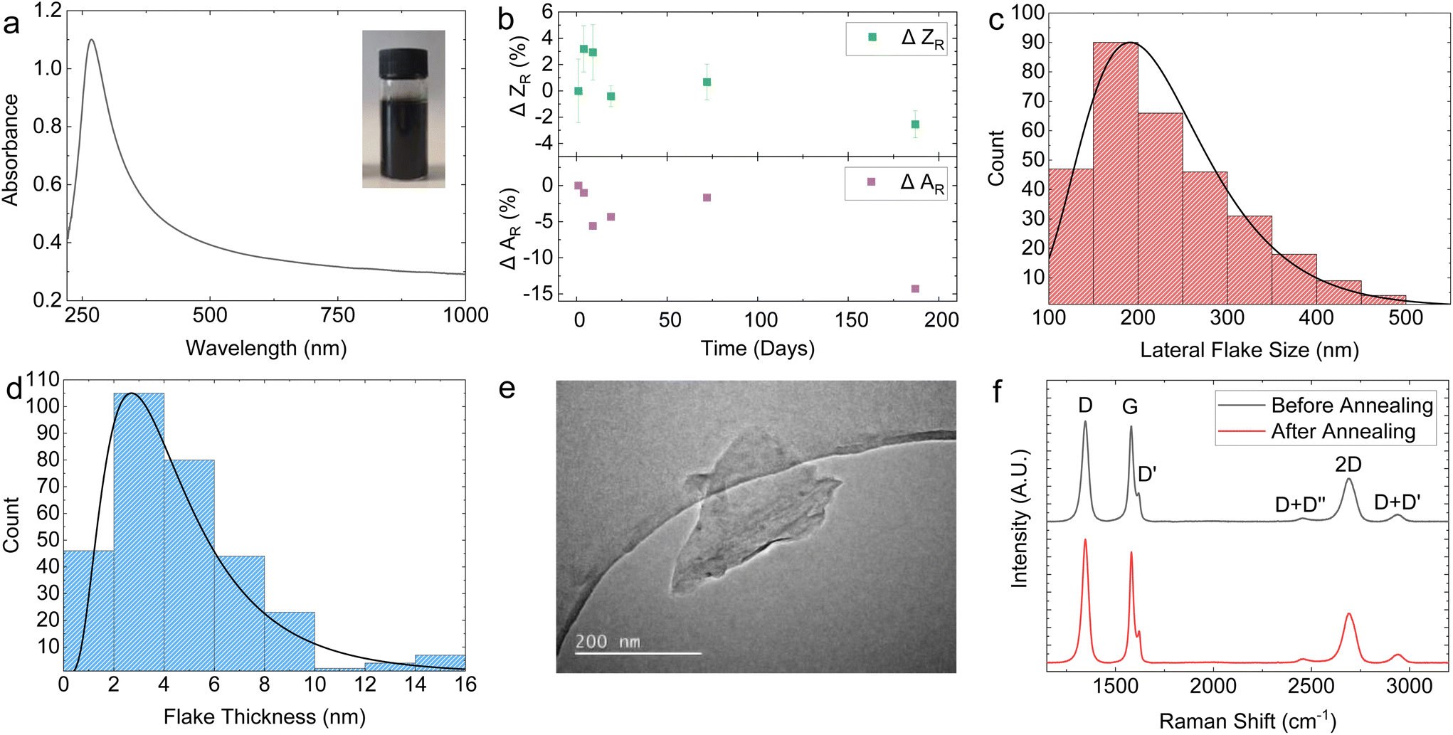 | ||
| Fig. 1 (a) OAS of the LPE graphene ink diluted by a factor of 61. (b) DLS and OAS stability analysis. DLS indicates stability against aggregation, with <3% decrease in relative size over 190 days whilst UV-Vis indicates gradual sedimentation initiating after 72 days of storage, peaking at −14.8% at day 190. (c) AFM statistics showing a log-normal distribution of 〈S〉 peaking at 190 nm. (d) AFM statistics showing a log-normal distribution of 〈t〉 peaking at 2.65 nm, which equates to a mean of 5-layer thick graphene when adjusted for a 1 nm water layer. (e) TEM image of a typical LPE graphene flake before photonic annealing. (f) Raman spectra before and after photonic annealing. | ||
The rheology of the graphene ink is investigated to assess its suitability for spray coating. The surface tension (γ) of the prepared graphene ink was γ ∼ 18.50 ± 0.25 mN m−1 (Fig. S2†), lower than ∼20.34 mN m−1 for pure 2-propanol at 25 °C, due to the added PVP stabiliser. Conversely, the resulting dynamic viscosity η ∼ 2.35 ± 0.1 mPa s is higher than ∼2.01 mPa s for the pure 2-propanol70 due to the presence of the stabiliser and the concentration of the graphene flakes.
The long-term stability of the graphene ink is an important parameter for reliable spraying and was investigated using OAS as precipitation of the ink would result in a lower concentration and absorbance, and with dynamic light scattering (DLS) to monitor the size and possible aggregation of the flakes. The Stokes–Einstein relation is used to estimate the average particle size in a dispersion, under the assumption of spherical particle shape, obtaining the intensity-weighted mean hydrodynamic size (Z).71 This makes, in principle, DLS unreliable to measure the average particle size of non-spherical flakes, such as in our case. However, it is possible to infer changes in the distribution of the dispersed flakes in our graphene ink caused by sedimentation or aggregation using DLS by monitoring changes in the relative Z (ZR). For instance, an increase in the mean ZR would indicate aggregate formation. Fig. 1b (top panel) plots the change in ZR (ΔZR) with time, represented as the percentage change with respect to ZR at the time of ink preparation. The graph shows that within a 190-day period, ΔZR ∼ −2.5 ± 1%, suggesting that only a minimal aggregate formation happens. Moreover, the graphene ink shows a monodisperse flake size profile indicated by a single peak in DLS measurement (Fig. S3a†). We also observed that the change in absorbance normalised to day 0 (ΔAR) was ∼−14% over a 190-day period (Fig. 1b, bottom panel), further demonstrating the stability of our graphene ink.
Fig. 1c and d show the atomic force microscopy (AFM) statistics (over 300 flakes) of the modal lateral flake size (〈S〉) and thickness (〈t〉), respectively, measured for our graphene ink deposited on a Si/SiO2 substrate. Both the 〈S〉 and 〈t〉 have a log-normal distribution, which peak at 〈S〉 ∼ 190 nm (Fig. 1c) and 〈t〉 ∼ 2.65 nm (Fig. 1d), respectively. Assuming a water-layer flake thickness of 1 nm (ref. 72) and a graphene interlayer distance of 0.34 nm,73 we obtain a mean flake thickness of 5 layers, indicating the graphene ink is composed of a combination of single-layer graphene (SLG) and few-layer graphene (FLG) flakes. This corresponds to an aspect ratio (Ar) of ∼67 which is higher than that reported for graphene-NMP inks (〈S〉 = 121 nm, 〈t〉 = 6 nm, Ar = 20) under similar exfoliation conditions.74 The 〈S〉 is also measured using scanning electron microscopy (SEM) (Fig. S4†). A sample of 70 flakes was measured, obtaining a lognormal distribution peaking at 〈S〉 ∼ 182 nm which closely aligns with the values obtained from the AFM statistics. Transmission electron microscopy (TEM) was further used to image individual flakes, with a representative flake size of 〈S〉 ∼ 200 mm shown in Fig. 1e.
The quality of the SLG and FLG flakes were monitored using Raman spectroscopy. Fig. 1f shows typical Raman spectra of the graphene ink deposited on SiO2, before and after photonic annealing (black and red curve respectively) to monitor any effect of the photonic annealing on the SLG/FLG flakes. The red and the black curves in Fig. 1f show the typical D peaks at ∼1346 cm−1, the 2D peaks at ∼2690 cm−1, and the G peaks at ∼1581 cm−1 (red) and 1580 cm−1 (black) respectively. The D peak shows a full-width at half maximum (FWHM) of 37.9 cm−1 (red) and 38.9 cm−1 (black). These values are consistent with those reported for LPE graphene inks,44,46,49 indicating the high quality of the SLG and FLG flakes in the graphene inks and the absence of noticeable modification of the flakes upon photonic annealing.
Device fabrication
Using a 6-step manufacturing process (Fig. 2), we developed a PCB test strip composed of two EG-GFET layouts (enabling up to two simultaneous EG-GFET measurements), each containing 4 electrodes – drain, source, gate, and quasi-reference (QR) (Fig. 3a). The test strip is manufactured using commercial PCB techniques on a glass-epoxy laminate substrate (FR-4). The EG-GFET source and drain interdigitated electrodes are comprised of 14 fingers, each 100 μm wide, resulting in a channel with 100 μm length and 2500 μm width (Fig. 3b). The overall channel area is 3.25 mm2. The gate and QR electrodes are 1.25 × 0.75 mm rectangles, and the QR electrode is covered with Ag/AgCl paste. The electrical connections to all electrodes are achieved using 2.54 mm-spaced gold-plated contacts, designed to fit into standard card edge connectors.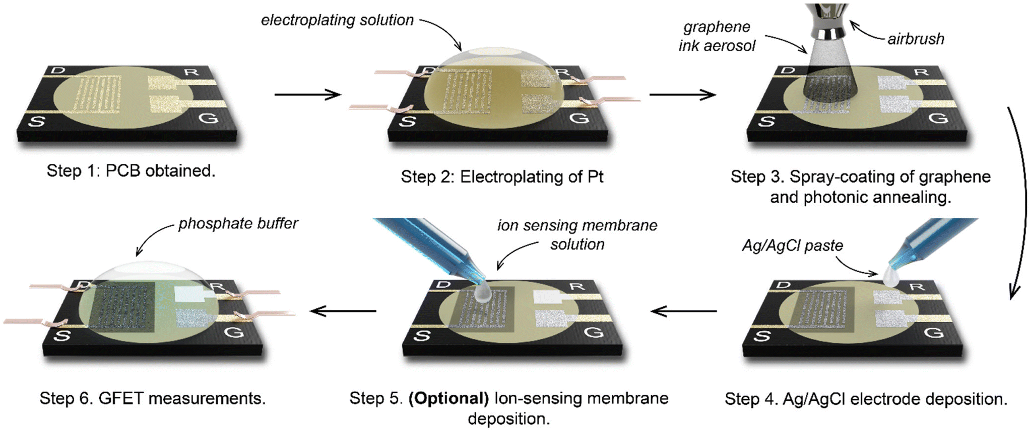 | ||
| Fig. 2 The manufacturing process to make four-terminal graphene PCB transistors for chemical sensing. | ||
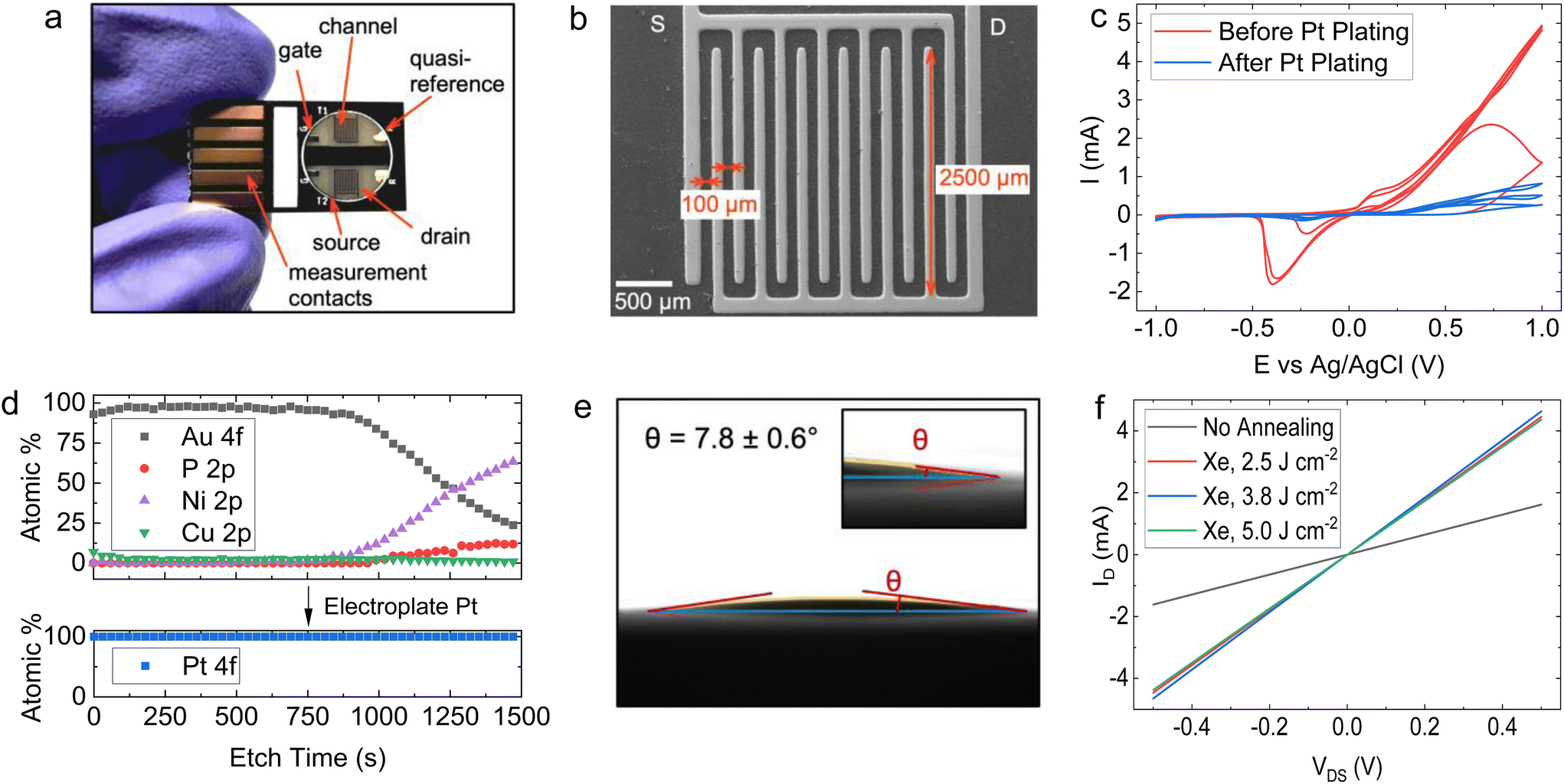 | ||
| Fig. 3 (a) Photograph of the GFET on PCB. (b) SEM micrograph of the interdigitated electrodes. (c) Cyclic voltammetry between −1 and 1 V using the original ENIG plated electrodes and Pt-plated electrodes, showing the nickel redox peaks and substantially greater stability of the Pt electrodes. (d) Depth profile of ENIG (top) and Pt (bottom) plating of the PCB. The approximate depth after 1500 seconds is 120 nm (0.08 nm s−1). (e) Contact angle of a drop of the graphene ink on a PCB substrate, showing a contact angle of θ = 7.8 ± 0.6°. (f) ID–VDS curves for the graphene channel showing a change in resistance after IPL annealing. The electrodes were dry (not in a solution) during the measurement. The resistances were 309.8 Ω (not annealed) and 112.4, 107.9 and 114.7 Ω for light pulse energies of 2.5 J cm−2, 3.75 J cm−2 and 5 J cm−2, respectively. | ||
Under ideal circumstances, the electrode surface must be inert under standard sensing conditions, to reduce the occurrence of undesirable chemical interference.75 The surface of the PCB test strip electrodes is plated with a 4 μm layer of nickel and a 75 nm layer of gold in a commercial electroless process (ENIG) to ensure the inertness of the electrodes, similar to the process in ref. 76. However, clear Faradaic peaks from oxidation (at positive potentials vs. Ag/AgCl reference) and reduction (−0.4 V vs. Ag/AgCl) of nickel or copper were observed (Fig. 3c, red curve) upon running cycling voltammetry in 10 mmol L−1 phosphate buffer with the gate electrode as the working electrode and a carbon rod as the counter electrode. This experiment simulates the potentials the electrodes would be exposed to during EG-GFET measurements and, ideally, no peaks indicating the corrosion of the electrodes would be observed. The red curve in Fig. 3c shows that even at a low voltage of 0.3 V vs. Ag/AgCl, the electrodes would start to dissolve, interfering with the EG-GFET sensing. XPS depth profiling of the electrodes to approximately 120 nm depth revealed the presence of copper throughout (Fig. 3d, top) in addition to gold, likely coming from an uneven coverage of the gold layer. A layer containing nickel and phosphorus was observed approximately 80 nm below the surface which is expected. The ENIG gold plating process is primarily intended to improve the solderability of the PCBs rather than provide electrochemically inert electrodes, as reported previously.77 Therefore, a 0.5 μm-thick layer of platinum was electroplated onto all the electrodes, to render them inert (Fig. 2, step 2). XPS profiling the electroplated electrodes shows the presence of only pure platinum in the top 120 nm (Fig. 3d, bottom) and the cyclic voltammetry sweeps (Fig. 3c blue curve) show substantially reduced Faradaic currents, typically associated with water electrolysis on platinum electrodes.78
The EG-GFET channel is formed by automatic spray-coating (see ‘Methods’) to ensure repeatable and scalable deposition of graphene ink onto the PCB test strip (Fig. 2 step 3). The contact angle between the ink and the PCB surface was only 7.8 ± 0.6° (Fig. 3e) and shows excellent wetting which contributes to film uniformity as the individual drops coalesce into a thin film before evaporating.45 Furthermore, increasing the atomisation gas pressure, which is applied on the liquid being ejected from the nozzle, decreases the average droplet size of graphene ink, which contributes to the formation of films with uniform thickness by depositing a larger number of smaller droplets.45,60 Therefore, the maximum pressure (275 kPa) permitted by the setup was used. The distance between the airbrush and the substrate (40 mm) was chosen such that the spray cone covered the entire area of the channel in a single pass. The spray rate was adjusted such that the film dried between the passes and the total volume of the ink was kept constant at 0.4 mL to obtain approximately 100 Ω channel resistivity after photonic annealing. The repeatability of the spray coating is shown in Fig. S5 in ESI,† demonstrating an 8% standard deviation with respect to the mean electrical resistance of the sensor batch.
We investigated the effect of photonic annealing on the electrical resistance of the EG-GFET channel by exposing the PCB test strip to three different IPL energies (Fig. 3f). Xenon IPL exposure at 2.5 J cm−2, 3.75 J cm−2 and 5.0 J cm−2 resulted in a similar decrease of the resistance from 309.8 Ω (not annealed, red curve) to 112.4, 107.9 and 114.7 Ω for light pulse energies of 2.5 J cm−2, 3.75 J cm−2 and 5.0 J cm−2, respectively. Therefore, the lowest IPL energy (2.5 J cm−2) was used for all subsequent experiments, ensuring improved channel resistance with minimal risk of damage to the PCB.
Device operation
The modular design of the PCB test strip increases the versatility of our platform – multi-sensor array test strips can be designed by multiplexing several EG-GFETs on the same PCB by proportionally increasing the quantity of source, drain electrodes. The EG-GFETs were contacted for electrical characterisation as shown in Fig. 4a. The QR electrode was connected to a high input impedance terminal (>1 GΩ source meter unit input impedance) to ensure no current flows through it. Additionally, we measured the current flowing through the source, drain and gate electrodes to ensure a complete understanding of the device response (whether the observed current changes are actual modulation of the graphene channel or not), as recommended by ref. 79.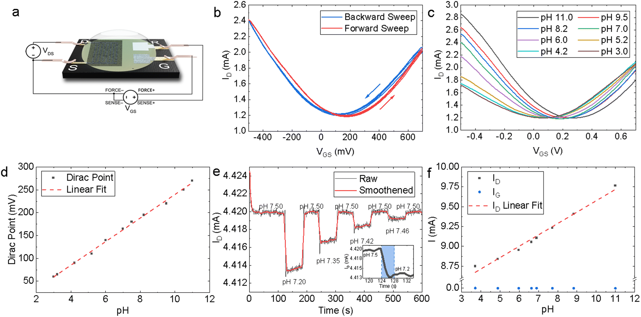 | ||
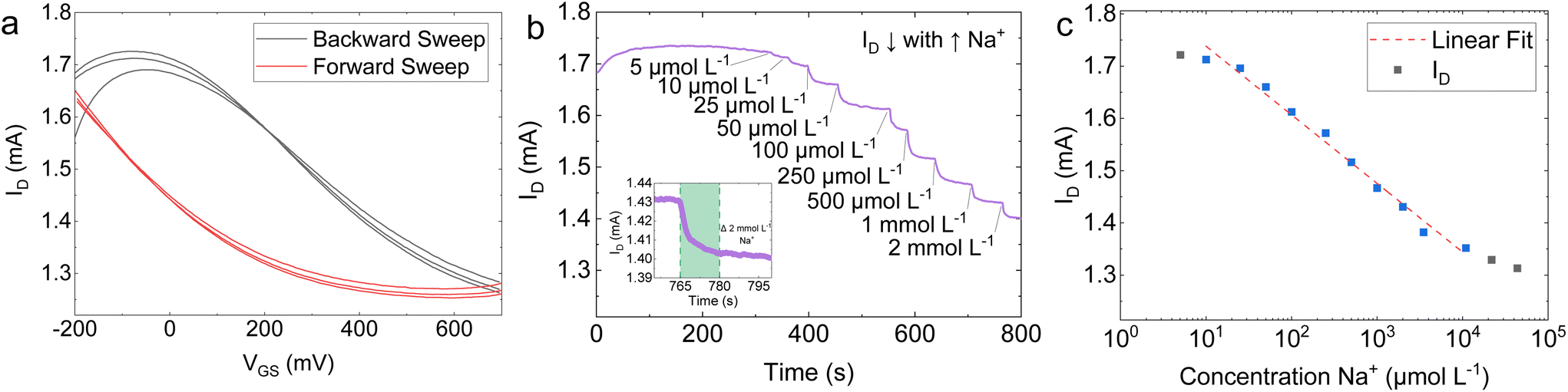
| Fig. 4 (a) Schematic of the four-terminal EG-GFET. (b) Forward and backward IDvs. VGS sweeps of the EG-GFET in 10 mmol L−1 PB solution at VDS = +200 mV. (c) Forward sweeps of the IDvs. VGS of the EG-GFET at decreasing pH values from pH 11 to pH 3. (d) The Dirac point values extracted from the plots in (c) showing a linearity of 25.8 ± 0.5 mV per pH. (e) pH switching showing an ultimate resolution of 0.04 pH units, with response times of <10 s. (f) ID sensitivity of 143 μA per pH through a linear range of pH 11 to pH 3 which is >2800 times greater than the IG response. | ||
Our EG-GFETs were initially characterised in phosphate buffer (PB) solutions of 10 mmol L−1 which is chosen as it provides a wide pH buffer range at around pH 7.80Fig. 4b shows the measured drain current (ID) plotted as a function of the gate voltage (VGS) at VDS = +200 mV, over three forward (red curve) and backward (blue curve) VGS sweep cycles between −500 and +700 mV, demonstrating a typical ambipolar graphene field-effect behaviour at a fixed pH value of 7. The Dirac point (also referred to as the charge neutrality point or CNP) of the device at pH 7 is found at VGS = +170 mV and 130 mV for the forward sweep and backward sweep curves, respectively, showing a hysteresis of 40 mV. The hysteresis observed is a well-known phenomenon in EG-GFETs. Computational modelling and Raman spectroscopy studies of the graphene-solution electrochemistry have suggested that the hysteresis is caused at least in part by electrochemical processes in the aqueous layer in contact with graphene.81,82 The electrochemical reduction of oxygen, O2 + 2H2O + 4e− = 4OH−, occurs spontaneously at the graphene–water interface and it is thought to be the primary source of interference.81,83 Reducing the dissolved oxygen content will result in a decrease in IG and hysteresis but purging samples of dissolved oxygen would not be practical for real-world analysis at the point-of-care.84 Consequently, we have arbitrarily chosen to conduct any further analysis on the EG-GFET sweep characteristics using the forward sweep, given the hysteresis effect does not appear to manifest in any drastic capacity at constant VGS.
We then investigated the response of the EG-GFETs to changes in pH by changing the pH of the solution using a strong base or acid and monitoring the response. Fig. 4c plots the ID as a function of VGS of the EG-GFETs exposed to pH values ranging from 3 to 11 under a VDS = +200 mV, which shows a shift of the Dirac point from 60 mV to 270 mV. Whilst pristine (defect-less) graphene should not respond to changes in pH,85 the pH sensitivity is enabled by the type and density of unintentional defects imparted during the LPE process.86 The corresponding pH-dependent shift in the Dirac point is shown in Fig. 4d, with a maximum Dirac point of 270 mV at pH 11. A linear fit of the Dirac point values (red dashed line) reveals a sensitivity of 25.8 ± 0.5 mV per pH, over a linear range of pH 11 to pH 3. This sensitivity is below the theoretical maximum predicted by the Nernst eqn (59.16 mV per pH)87 and is higher than that observed for graphene pH sensors prepared by alternative graphene fabrication techniques such as CVD-grown graphene on SiO2 (21–22 mV per pH),88 suspended graphene (17 mV per pH),89 epitaxial graphene on silicon carbide (19 mV per pH)90 and mechanically exfoliated graphene on SiO2 (20 mV per pH),91 and within the same order of magnitude for reduced graphene oxide (rGO) based devices (29–40 mV per pH).92,93
We also use the VGS sweeps to identify the ideal VGS value for constant VGS sensing. A VGS value of +50 mV was chosen for pH sensing as it is in the linear regime of the ID response and is also the VGS at which the minimum magnitude of IG occurs (Fig. S6†). The EG-GFET resolution to pH sensing is ultimately limited by the noise of the measurement setup.94 Hence minimising IG is integral to minimising noise and drift, improving device lifespan, and ensuring robustness.84,95
Fig. 4e shows the response of ID (at VGS = +50 mV and VDS = +200 mV) as a function of time to diminishing alternate additions of acid and base, which change the pH of the measured solution. The baseline peak-to-peak ID noise is IDnoise, P–P ∼ 1 μA whilst root mean square (RMS) ID noise is IDnoise, RMS ∼ 0.2 μA. Adjusting the pH from 7.50 to 7.20 caused ID to drop from 4.420 mA to 4.414 mA. The inset in Fig. 4e shows a zoomed-in region of the same plot for a pH change of 0.30 (blue shading) that we used to estimate the response time as τr ∼ 4 s. Subsequent adjustment of the pH from 7.20 back to 7.50 caused ID to return to 4.420 mA. The resolution R was determined by measuring ID over subsequent additions of acid and base in diminishing quantities, yielding R ∼ 0.04 pH units for the EG-GFET. Both τr and R are in line with previously reported pH-sensitive EG-GFET devices,96 demonstrating the suitability of our platform for commercial, scalable, and low-cost manufacturing techniques with superior performance characteristics to those based on CVD88 and mechanical exfoliation.91
The sensitivity of the device may alternatively be described as a function of change in ID, at constant VGS and VDS. Fig. 4f shows a plot of ID values (black data points) as a function of pH at VDS = +200 mV and VGS = +50 mV. A linear fit (red dashed line) of the ID points, shows a sensitivity of 143 ± 7 μA per pH through a dynamic range of pH 11.0 to 3.0. The sensitivity of ID to pH is over three orders of magnitude higher than the sensitivity of IG (blue data points), which is 0.05 ± 0.02 μA per pH over the same range, thus excluding the possibility of electrolysis playing a significant role in the sensor response to pH.79 Moreover, we demonstrated multiple EG-GFETs detecting for pH (N = 10) from 5 separate fabrication batches. The EG-GFETs were allowed to settle for 180 s to attain a stable ID (Fig. S7†). The EG-GFETs show a mean pH sensitivity of sensitivity 3.05 ± 0.15% per pH unit (Fig. S8†), between pH 3 and 11, with high precision and low variance (adjusted R2 = 98.04%).
The utility of EG-GFETs resides in their versatility towards targeted detection of further species beyond H3O+/OH− (pH). We tested the suitability of our platform to detect Na+ by depositing a sodium-selective membrane as a proof-of-concept of the platform's potential use for ion-selective detection applications.97,98 A thin polyvinyl chloride (PVC)-based ion selective membrane (ISM) impregnated with ‘sodium ionophore X’ (see ‘Methods’) was deposited on top of the graphene channel of the EG-GFET. In general, ion-selective EG-GFETs respond to the activity of the target ion with a higher sensitivity than other species, allowing for targeted measurements.97 The extent of this selectivity depends on a range of factors including the membrane and analyte compositions.99 In the ion-selective EG-GFET, a change of potential is experienced at the surface of the EG-GFET channel, which in turn is observed as a shift in the Dirac point and a subsequent change in ID.100
The ion-selective EG-GFET was operated using the same electrical schematic shown in Fig. 4a. Fig. 5a shows three cycles of ID plotted against the gate voltage (VGS) in a 10 mmol L−1 potassium phosphate buffer (K-PB) solution, with the forward sweep (black curve) going from −500 mV to +700 mV and the backward sweep (red curve) going from +700 mV to −500 mV. The Dirac point is substantially broadened when compared to the membrane-less EG-GFET shown in Fig. 4b. Additionally, Fig. 5a shows an increased hysteresis between the forward and backward sweeps, resulting in the Dirac point shift for the forward sweep of more than +700 mV with respect to Ag/AgCl. However, the increased hysteresis did not influence the device performance, as Na+ quantification was conducted at constant VGS.
 | ||
| Fig. 5 (a) Sweep of a Na+-selective EG-GFET in 10 mmol L−1 K-PB. (b) Incremental addition of Na+ results in a proportional decrease in the ID. (c) The GFET response to Na+ is 131.4 ± 5 μA per log10 change in Na+ in the range of 5 μmol L−1 to 10 mmol L−1. | ||
Fig. 5b shows a decreasing ID in response to incremental additions of Na+ to the ion selective EG-GFET at VDS = +200 mV and VGS = +50 mV. The LOD was measured as 5 μmol L−1 for Na+. The inset in Fig. 5b shows a zoomed-in region of the same plot for a change of 2 mmol L−1 Na+ (green shading) that we used to estimate τr ∼ 15 s, within the linear range of the ion selective EG-GFET. A plot of the ID response as a function of Na+ concentration is plotted in Fig. 5c. The Na+ selective EG-GFET has a limit of quantification (LOQ) of 20 μmol L−1, with a log-linear response running from 20 μmol L−1 to 10 mmol L−1 (red dashed line) defining the device's linear range. The sensitivity of the device is extracted from the slope of the response in Fig. 5b, which shows a sensitivity of 131.4 ± 5 μA per log10Na+. These performance metrics are in line with the best sodium selective GFETs previously reported using CVD graphene.100,101 Furthermore, we demonstrated 2 Na+-selective EG-GFETs simultaneously detecting Na+. The EG-GFETs were allowed to settle for 300 s to attain a stable ID (Fig. S9†). The EG-GFETs show a mean Na+ sensitivity of −6.58 ± 0.19% per log10 change in Na+ concentration, between 5 μmol L−1 and 10 mmol L−1, with high precision and low variance (adjusted R2 = 99.43%).
The ion-selective EG-GFETs may be tuned by adjusting the chemical and physical composition of the ISMs, thus tailoring devices to meet specific application criteria for ion sensing. The versatility of ion selective detection is immediately evident for its utility in health but may also be of further use in environmental monitoring and veterinary care.102 Moreover, our two pH and ion-selective EG-GFETs on the same PCB test strip demonstrate a platform structure that allows for the fabrication of multiple sensors which can detect multiple analytes within a sample, paving the way for high-performance, scalable commercial sensors for low-cost and real-time diagnostics.
3. Methods
Formulation of LPE Graphene Inks
50 mg mL−1 of graphite (Ceylon) were added to 0.4 mg mL−1 of polyvinyl-pyrrolidone (PVP) (Merck, average Mw = 40000) in 2-propanol (Sigma Aldrich, ACS reagent ≥99.8% purity). The graphite was exfoliated by immersion of the mixture in a bath sonicator (Fisherbrand Elmasonic S150 Ultrasonication Unit, 300 W effective power) for 9 hours. The resultant dispersion was subsequently centrifuged (Beckman Allegra 64R, F06050 Fixed-Angle Rotor) at 13000g (mean) for 1 hour. After centrifugation, the top 80% of the supernatant was retained as the LPE graphene ink.
Characterisation techniques
Raman spectra were measured on a Renishaw inVia micro-Raman spectrometer (WiRe 4.1) using a ×20 objective with a green 532 nm laser and 1800 lines per mm grating. An incident power of ≤1 mW was used to avoid thermal damage. Samples for Raman spectroscopy were deposited as thin films on Si/SiO2 (Si-Mat, 200 nm dry thermal oxide).
Dynamic light scattering (DLS or photon correlation spectroscopy, PCS) was carried out on a Zetasizer Ultra. The scattering angle was set to 175°. Dispersions were freshly diluted in 0.4 mg mL−1 PVP in IPA. Measurements were collected at 25 °C with 60 s of settling time. Stability assays were conducted by storing aliquots of inks in Eppendorf tubes under ambient conditions. Aliquots were retrieved over time and diluted for analysis. A dilution factor of 61 was determined by identifying the ink concentration range which yielded a constant Z average (Fig. S3b†). In the ink stability assays, the intensity-weighted mean hydrodynamic size (Z) of the population of particles in a dispersion was used to infer changes in the distribution of SLGs and FLGs (brought about by sedimentation or aggregation) by monitoring the relative changes in Z with time, in conjunction with the sample's polydispersity. The relative Z (ZR) is defined as Z normalised to Z at day 1. Subsequently, ΔZR is defined as ΔZR = ZR−1 − ZR−X, where ZR−1 and ZR−X are the ZR at day 1 and day x respectively.
Atomic force microscopy (AFM) measurements were performed using the Asylum Research MFP 3D Scanning Probe Microscope. Measurements were collected in tapping mode using a general-purpose silicon AFM probe (Nunano SCOUT 70), with a 70 kHz resonance frequency and tip radius curvature of <10 nm. LPE graphene dispersions were diluted to 0.01 mg mL−1 and deposited on Si/SiO2 (Si-Mat, 200 nm dry thermal oxide). Prior to deposition, the Si/SiO2 wafers were cleaned of insoluble organic contaminants using a 5:1:1 mixture of deionised water, 30% (w/w) H2O2 (Merck) and 25% ammonium hydroxide solution in water (Acros Organics, extra pure) at 80 °C for 10 minutes.104 AFM analysis was carried out using Gwyddion (v 2.58). The mean flake size 〈S〉, is calculated as  , where x and y are the length and width of the flakes74 and n is the number of flakes, while mean flake thickness 〈t〉 is calculated by averaging the flake thickness at the thickest point for each flake. The aspect ratio (Ar) was defined as 〈S〉/〈t〉.
Device fabrication
:1 dilution in THF was conducted to produce a solution of 8 mg mL−1. The solution was stored at 2–8 °C.
The ion selective solution was deposited on top of the transistor by drop casting 5 μL of the 8 mg mL−1 solution onto the transistor and allowed 30 seconds to dry. A further 2.5 μL of 80 mg mL−1 was then deposited on top. The ion selective membrane (ISM) was allowed to dry for 12 hours in ambient conditions. Prior to first characterisation, the membraned devices were immersed for 15 minutes in a solution 0.1 mol L−1 NaCl (VWR, ACS reagent) followed by a 10-minute rinse in deionised water. The sodium selective sensors were reused by dipping them in deionised water for 10 minutes.
Device measurements
Peak to peak noise measurements were measured by measuring the difference between the maximum and minimum values within a region where no response signal is expected. Alternatively, the RMS noise was measured as the standard deviation of the baseline noise since mean of a noise signal is zero.
Detection for sodium ions was conducted by sequential additions of Na2SO4 (VWR, ≥98% purity) solutions in deionised water or potassium phosphate buffer solution (K-PB). K-PB was prepared by dissolving 7.541 mmol of potassium phosphate dibasic, K2HPO4, (Sigma Aldrich, ACS reagent, ≥98% purity) and 2.459 mmol of potassium phosphate monobasic, KH2PO4, (Sigma Aldrich, ACS reagent, ≥99%) in 1 L of deionised water.
For each detected analyte, the relevant device performance characteristics were established, in line with existing protocols.108,109 The sensitivity is defined as the change in the device response divided by the corresponding change in stimulus, which is also expressed as the slope of the signal to stimulus.108,109 The limit of detection (LOD) is the lowest amount of analyte that can be detected whilst the limit of quantification (LOQ) is the lowest amount of analyte that can be quantified.108 The limit of quantitation (or quantification) is the analytical value above which greater values can be quantified.108 The linear range is the range of analyte concentrations at which the signal response is linearly proportional to the concentration of analyte.108 The resolution (R) is defined as the lowest difference in concentration that can be distinguished on constant changes.109 The response time (τr) is the time for a sensor to respond from a stable concentration of analyte to a step change in concentration.109 Hysteresis is the maximum difference in output when a value is separately approached via increasing and decreasing analyte concentration ranges109 or the maximum change in output between forward and backward VGS sweeps at the same concentration.
4. Conclusions
This works demonstrates the first application of sprayed graphene transistors for test strips within a lab-on-PCB architecture for the detection of pH and selective ion sensing. We document a step-by-step procedure that makes use of commonly available chemicals, components, and techniques for the fabrication of commercially viable, scalable, and low-cost chemical sensors and biosensors. By combining the production of graphene inks with spray coating, we can produce graphene transistor devices on PCB substrates. The test strips demonstrate sensing of pH between pH 3 and 11, with a resolution of 0.04 pH units, a response time of <10 seconds and a sensitivity of 25.8 mV per pH, which is in line with the state-of-the-art performances obtained using mechanically exfoliated and CVD-grown graphene. Finally, we also demonstrate the deposition of selective ion membranes on the surface of the graphene transistor for the detection of sodium as a proof-of-principle structure, with a sensitivity of 131 ± 4 μA per log10[Na+] through a linear range of 5 μmol L−1 to 10 mmol L−1, setting the ground for commercially viable PCB-based sensor arrays.Author contributions
BFS and MH conceived and conducted the experiments, analysed the results, contributed to result interpretation and procedural validation. BFS also conducted the literature search. CY contributed to the characterisation of materials. FT directed the project, contributed to result interpretation and to procedural validation. BFS, MH, AEGC and FT wrote the manuscript with input from all the authors.Conflicts of interest
The authors have no conflicts of interest to declare.Acknowledgements
The authors would like to thank Prof. Milo Shaffer for access to the Raman spectroscopy suite, Dr Nicola Gasparini for his assistance with the electrical measurements. MH acknowledges funding from Imperial College President’s PhD Scholarship (EPSRC EP/T51780X/1) and support by the EPSRC Centre for Doctoral Training in Advanced Characterisation of Materials (EPSRC EP/S023259/1). CY acknowledges funding from the China Scholarship Council. The authors acknowledge support from EPSRC grants EP/P02534X/2, EP/R511547/1 and EP/T005106/1, and the Imperial College Collaboration Kick-Starter grant.References
- A. van Belkum, T. T. Bachmann, G. Lüdke, J. G. Lisby, G. Kahlmeter, A. Mohess, K. Becker, J. P. Hays, N. Woodford, K. Mitsakakis, J. Moran-Gilad, J. Vila, H. Peter, J. H. Rex and W. M. Dunne, Nat. Rev. Microbiol., 2019, 17, 51–62 CrossRef CAS PubMed.
- A. A. Souza, C. Ducker, D. Argaw, J. D. King, A. W. Solomon, M. A. Biamonte, R. N. Coler, I. Cruz, V. Lejon, B. Levecke, F. K. Marchini, M. Marks, P. Millet, S. M. Njenga, R. Noordin, R. Paulussen, E. Sreekumar and P. J. Lammie, Trans. R. Soc. Trop. Med. Hyg., 2021, 115, 129–135 CrossRef PubMed.
- P. A. Lieberzeit and F. L. Dickert, Anal. Bioanal. Chem., 2009, 393, 467–472 CrossRef CAS PubMed.
- S. Li, A. Simonian and B. A. Chin, Electrochem. Soc. Interface, 2010, 19, 41–46 CrossRef CAS.
- N. Graber, H. Lodi and H. M. Widmer, Sens. Actuators, B, 1990, 239–243 CrossRef CAS.
- A. Vasilescu, P. Fanjul-Bolado, A. M. Titoiu, R. Porumb and P. Epure, Chemosensors, 2019, 7(4), 66 CrossRef CAS.
- K. J. Land, D. I. Boeras, X. S. Chen, A. R. Ramsay and R. W. Peeling, Nat. Microbiol., 2019, 4, 46–54 CrossRef CAS PubMed.
- J. Janata, Principles of Chemical Sensors, 2009 Search PubMed.
- D. Grieshaber, R. MacKenzie, J. Vörös and E. Reimhult, Sensors, 2008, 8, 1400–1458 CrossRef CAS PubMed.
- H. Lee, Y. J. Hong, S. Baik, T. Hyeon and D. H. Kim, Adv. Healthc. Mater., 2018, 7, 1701150 CrossRef PubMed.
- Ö. Isildak and O. Özbek, Crit. Rev. Anal. Chem., 2021, 51, 218–231 CrossRef PubMed.
- S. Das and V. Jayaraman, Prog. Mater. Sci., 2014, 66, 112–255 CrossRef CAS.
- T. Yang, R. Yu, Y. Yan, H. Zeng, S. Luo, N. Liu, A. Morrin, X. Luo and W. Li, Sens. Actuators, B, 2018, 274, 501–516 CrossRef CAS.
- E. Sehit and Z. Altintas, Biosens. Bioelectron., 2020, 159, 112165 CrossRef CAS PubMed.
- J. Heikenfeld, A. Jajack, J. Rogers, P. Gutruf, L. Tian, T. Pan, R. Li, M. Khine, J. Kim, J. Wang and J. Kim, Lab Chip, 2018, 18, 217–248 RSC.
- A. J. Bandodkar, I. Jeerapan and J. Wang, ACS Sens., 2016, 1, 464–482 CrossRef CAS.
- H. Karimi-Maleh, F. Karimi, M. Alizadeh and A. L. Sanati, Chem. Rec., 2020, 20, 682–692 CrossRef CAS PubMed.
- B. Zhan, C. Li, J. Yang, G. Jenkins, W. Huang and X. Dong, Small, 2014, 10, 4042–4065 CrossRef CAS PubMed.
- N. S. Green and M. L. Norton, Anal. Chim. Acta, 2015, 853, 127–142 CrossRef CAS PubMed.
- M. Kaisti, Biosens. Bioelectron., 2017, 98, 437–448 CrossRef CAS PubMed.
- E. W. Hill, A. Vijayaragahvan and K. Novoselov, IEEE Sens. J., 2011, 11, 3161–3170 CAS.
- V. Georgakilas, M. Otyepka, A. B. Bourlinos, V. Chandra, N. Kim, K. C. Kemp, P. Hobza, R. Zboril and K. S. Kim, Chem. Rev., 2012, 112, 6156–6214 CrossRef CAS PubMed.
- G. P. Nikoleli, Z. H. Ibupoto, D. P. Nikolelis, V. Likodimos, N. Psaroudakis, N. Tzamtzis, M. Willander and T. Hianik, Cent. Eur. J. Chem., 2013, 11, 1554–1561 CAS.
- J. Ping, Y. Wang, K. Fan, W. Tang, J. Wu and Y. Ying, J. Mater. Chem. B, 2013, 1, 4781–4791 RSC.
- R. K. Paul, S. Badhulika, N. M. Saucedo and A. Mulchandani, Anal. Chem., 2012, 84, 8171–8178 CrossRef CAS PubMed.
- W. Fu, L. Jiang, E. P. van Geest, L. M. C. Lima, G. F. Schneider, W. Fu, L. Jiang, E. P. van Geest, L. M. C. Lima and G. F. Schneider, Adv. Mater., 2017, 29, 1603610 CrossRef PubMed.
- B. Zhan, C. Li, J. Yang, G. Jenkins, W. Huang and X. Dong, Small, 2014, 10, 4042–4065 CrossRef CAS PubMed.
- M. Khademi and D. P. J. Barz, Langmuir, 2020, 36, 4250–4260 CrossRef CAS PubMed.
- M. Zhang, C. Liao, C. H. Mak, P. You, C. L. Mak and F. Yan, Sci. Rep., 2015, 5, 1–6 CAS.
- H. U. Shihui, J. Zhang, Z. Wang and J. Yunfang, Chin. J. Electron., 2022, 31, 652–657 CrossRef.
- F. Chen, Q. Qing, J. Xia, J. Li and N. Tao, J. Am. Chem. Soc., 2009, 131, 9908–9909 CrossRef CAS PubMed.
- A. Schuck, H. E. Kim, J. K. Moreira, P. S. Lora and Y. S. Kim, Sensors, 2021, 21, 1–13 CrossRef PubMed.
- C. Wang, X. Cui, Y. Li, H. Li, L. Huang, J. Bi, J. Luo, L. Q. Ma, W. Zhou, Y. Cao, B. Wang and F. Miao, Sci. Rep., 2016, 6, 21711 CrossRef CAS PubMed.
- C. F. Wang, X. Y. Sun, M. Su, Y. P. Wang and Y. K. Lv, Analyst, 2020, 145, 1550–1562 RSC.
- B. Cai, S. Wang, L. Huang, Y. Ning, Z. Zhang and G. J. Zhang, ACS Nano, 2014, 8, 2632–2638 CrossRef CAS PubMed.
- R. Zhang and Y. Jia, J. Instrum., 2021, 16, P09021 CrossRef CAS.
- K. Maehashi, Y. Sofue, S. Okamoto, Y. Ohno, K. Inoue and K. Matsumoto, Sens. Actuators, B, 2013, 187, 45–49 CrossRef CAS.
- X. Li, W. Cai, J. An, S. Kim, J. Nah, D. Yang, R. Piner, A. Velamakanni, I. Jung, E. Tutuc, S. K. Banerjee, L. Colombo and R. S. Ruoff, Science, 2009, 324, 1312–1314 CrossRef CAS PubMed.
- Y. Zhang, L. Zhang and C. Zhou, Acc. Chem. Res., 2013, 46, 2329–2339 CrossRef CAS PubMed.
- Y. Hernandez, V. Nicolosi, M. Lotya, F. M. Blighe, Z. Sun, S. De, I. T. McGovern, B. Holland, M. Byrne, Y. K. Gun'ko, J. J. Boland, P. Niraj, G. Duesberg, S. Krishnamurthy, R. Goodhue, J. Hutchison, V. Scardaci, A. C. Ferrari and J. N. Coleman, Nat. Nanotechnol., 2008, 3, 563–568 CrossRef CAS PubMed.
- T. Hasan, F. Torrisi, Z. Sun, D. Popa, V. Nicolosi, G. Privitera, F. Bonaccorso and A. C. Ferrari, Phys. Status Solidi B, 2010, 2957, 2953–2957 CrossRef.
- F. Torrisi, T. Hasan, W. Wu, Z. Sun, A. Lombardo, T. S. Kulmala, G. W. Hsieh, S. Jung, F. Bonaccorso, P. J. Paul, D. Chu and A. C. Ferrari, ACS Nano, 2012, 6, 2992–3006 CrossRef CAS PubMed.
- K. R. Paton, E. Varrla, C. Backes, R. J. Smith, U. Khan, A. O'Neill, C. Boland, M. Lotya, O. M. Istrate, P. King, T. Higgins, S. Barwich, P. May, P. Puczkarski, I. Ahmed, M. Moebius, H. Pettersson, E. Long, J. Coelho, S. E. O'Brien, E. K. McGuire, B. M. Sanchez, G. S. Duesberg, N. McEvoy, T. J. Pennycook, C. Downing, A. Crossley, V. Nicolosi and J. N. Coleman, Nat. Mater., 2014, 13, 624–630 CrossRef CAS PubMed.
- P. G. Karagiannidis, S. A. Hodge, L. Lombardi, F. Tomarchio, N. Decorde, S. Milana, I. Goykhman, Y. Su, S. v. Mesite, D. N. Johnstone, R. K. Leary, P. A. Midgley, N. M. Pugno, F. Torrisi and A. C. Ferrari, ACS Nano, 2017, 11, 2742–2755 CrossRef CAS PubMed.
- T. Carey, C. Jones, F. le Moal, D. Deganello and F. Torrisi, ACS Appl. Mater. Interfaces, 2018, 10, 19948–19956 CrossRef CAS PubMed.
- F. Torrisi, T. Hasan, W. Wu, Z. Sun, A. Lombardo, T. S. Kulmala, G.-W. Hsieh, S. Jung, F. Bonaccorso, P. J. Paul, D. Chu and A. C. Ferrari, ACS Nano, 2012, 6, 2992–3006 CrossRef CAS PubMed.
- D. S. Kim, J. M. Jeong, H. J. Park, Y. K. Kim, K. G. Lee and B. G. Choi, Nanomicro Lett., 2021, 13, 1–14 CAS.
- E. Jabari and E. Toyserkani, Carbon, 2015, 91, 321–329 CrossRef CAS.
- T. Carey, S. Cacovich, G. Divitini, J. Ren, A. Mansouri, J. M. Kim, C. Wang, C. Ducati, R. Sordan and F. Torrisi, Nat. Commun., 2017, 8, 1–11 CrossRef CAS PubMed.
- E. B. Secor, P. L. Prabhumirashi, K. Puntambekar, M. L. Geier and M. C. Hersam, J. Phys. Chem. Lett., 2013, 4, 1347–1351 CrossRef CAS PubMed.
- S. Papamatthaiou, P. Estrela and D. Moschou, Sci. Rep., 2021, 11, 1–9 CrossRef PubMed.
- V. Nicolosi, M. Chhowalla, M. G. Kanatzidis, M. S. Strano and J. N. Coleman, Science, 2013, 340, 6139 CrossRef.
- IEC 60747-14-10:2019, Semiconductor sensors. Performance evaluation methods for wearable glucose sensors.
- N. Mavredakis, R. Garcia Cortadella, A. Bonaccini Calia, J. A. Garrido and D. Jiménez, Nanoscale, 2018, 10, 14947–14956 RSC.
- D. Moschou and A. Tserepi, Lab Chip, 2017, 17, 1388–1405 RSC.
- C. D. Chin, V. Linder and S. K. Sia, Lab Chip, 2012, 12, 2118–2134 RSC.
- H. J. Kim, K. A. Sudduth and J. W. Hummel, J. Environ. Monit., 2009, 11, 1810–1824 RSC.
- C. Zuliani and D. Diamond, Electrochim. Acta, 2012, 84, 29–34 CrossRef CAS.
- A. M. Zeidell, D. S. Filston, M. Waldrip, H. F. Iqbal, H. Chen, I. McCulloch and O. D. Jurchescu, Adv. Mater. Technol., 2020, 5, 2000390 CrossRef CAS.
- A. H. Lefebvre and V. G. McDonell, Atomization and Sprays, CRC Press, Boca Raton, 2nd edn, 2017 Search PubMed.
- I. M. Smallwood, Handbook of Organic Solvent Properties, 2012, pp. 1–306 Search PubMed.
- S. Bohm, A. Ingle, H. L. M. Bohm, B. Fenech-Salerno, S. Wu and F. Torrisi, Philos. Trans. R. Soc., A, 2021, 379, 2203 CrossRef PubMed.
- F. Torrisi and T. Carey, in Flexible Carbon-Based Electronics, ed. P. Samori and V. Palermo, Wiley-VCH, 2018, pp. 131–205 Search PubMed.
- M. Lotya, Y. Hernandez, P. J. King, R. J. Smith, V. Nicolosi, L. S. Karlsson, F. M. Blighe, S. De, W. Zhiming, I. T. McGovern, G. S. Duesberg and J. N. Coleman, J. Am. Chem. Soc., 2009, 131, 3611–3620 CrossRef CAS PubMed.
- A. B. Bourlinos, V. Georgakilas, R. Zboril, T. A. Steriotis, A. K. Stubos and C. Trapalis, Solid State Commun., 2009, 149, 2172–2176 CrossRef CAS.
- R. Narayan and S. O. Kim, Nano Convergence, 2015, 2, 1–19 CrossRef PubMed.
- B. K. Kandola, B. Biswas, D. Price and A. R. Horrocks, Polym. Degrad. Stab., 2010, 95, 144–152 CrossRef CAS.
- E. B. Secor, B. Y. Ahn, T. Z. Gao, J. A. Lewis and M. C. Hersam, Adv. Mater., 2015, 27, 6683–6688 CrossRef CAS PubMed.
- T. Stroucken and S. W. Koch, in Optical Properties of Graphene, ed. R. Bonder, World Scientific Publishing, 2016, pp. 43–84 Search PubMed.
- T. M. Aminabhavi, M. I. Aralaguppi, S. B. Harogoppad and R. H. Balundgi, J. Chem. Eng. Data, 1993, 38, 31–39 CrossRef CAS.
- D. López-Díaz, M. López Holgado, J. L. García-Fierro and M. M. Velázquez, J. Phys. Chem. C, 2017, 121, 20489–20497 CrossRef.
- P. Nemes-Incze, Z. Osváth, K. Kamarás and L. P. Biró, Carbon, 2008, 46, 1435–1442 CrossRef CAS.
- C. D. Reddy, S. Rajendran and K. M. Liew, Nanotechnology, 2006, 17, 864–870 CrossRef CAS.
- T. Carey, S. Cacovich, G. Divitini, J. Ren, A. Mansouri, J. M. Kim, C. Wang, C. Ducati, R. Sordan and F. Torrisi, Nat. Commun., 2017, 8, 1201 CrossRef PubMed.
- J. Barek, Chemosensors, 2021, 9, 1–15 CrossRef.
- A. Accogli, A. Lucotti and L. Magagnin, ECS Trans., 2017, 75, 1–6 CrossRef CAS.
- H. Shamkhalichenar, C. J. Bueche and J. W. Choi, Biosensors, 2020, 10, 159 CrossRef CAS PubMed.
- R. M. Cerviño, W. E. Triaca and A. J. Arvia, J. Electroanal. Chem. Interfacial Electrochem., 1985, 182, 51–60 CrossRef.
- J. Janata, ECS Solid State Lett., 2012, 1, M29 CrossRef CAS.
- A. A. Green, J. Am. Chem. Soc., 1933, 55, 2331–2336 CrossRef CAS.
- H. Pinto, R. Jones, J. P. Goss and P. R. Briddon, Phys. Status Solidi A, 2010, 207, 2131–2136 CrossRef CAS.
- H. Xu, Y. Chen, J. Zhang and H. Zhang, Small, 2012, 8, 2833–2840 CrossRef CAS PubMed.
- J. Wei, B. Liang, Q. Cao, H. Ren, Y. Zheng and X. Ye, Carbon, 2020, 156, 67–76 CrossRef CAS.
- A. Svetlova, D. Kireev, G. Beltramo, D. Mayer and A. Offenhäusser, ACS Appl. Electron. Mater., 2021, 3, 5355–5364 CrossRef CAS.
- W. Fu, C. Nef, O. Knopfmacher, A. Tarasov, M. Weiss, M. Calame and C. Schönenberger, Nano Lett., 2011, 11, 3597–3600 CrossRef CAS PubMed.
- W. Fu, C. Nef, A. Tarasov, M. Wipf, R. Stoop, O. Knopfmacher, M. Weiss, M. Calame and C. Schönenberger, Nanoscale, 2013, 5, 12104–12110 RSC.
- D. K. Harrison and W. F. Walker, J. Med. Eng. Technol., 1980, 4, 3–7 CrossRef CAS PubMed.
- B. Mailly-Giacchetti, A. Hsu, H. Wang, V. Vinciguerra, F. Pappalardo, L. Occhipinti, E. Guidetti, S. Coffa, J. Kong and T. Palacios, J. Appl. Phys., 2013, 114, 084505 CrossRef.
- Z. Cheng, Q. Li, Z. Li, Q. Zhou and Y. Fang, Nano Lett., 2010, 10, 1864–1868 CrossRef CAS PubMed.
- J. Ristein, W. Zhang, F. Speck, M. Ostler, L. Ley and T. Seyller, J. Phys. D: Appl. Phys., 2010, 43, 345303 CrossRef.
- Y. Ohno, K. Maehashi, Y. Yamashiro and K. Matsumoto, Nano Lett., 2009, 9, 3318–3322 CrossRef CAS PubMed.
- P. Salvo, N. Calisi, B. Melai, B. Cortigiani, M. Mannini, A. Caneschi, G. Lorenzetti, C. Paoletti, T. Lomonaco, A. Paolicchi, I. Scataglini, V. Dini, M. Romanelli, R. Fuoco and F. di Francesco, Biosens. Bioelectron., 2017, 91, 870–877 CrossRef CAS PubMed.
- I. Y. Sohn, D. J. Kim, J. H. Jung, O. J. Yoon, T. Nguyen Thanh, T. Tran Quang and N. E. Lee, Biosens. Bioelectron., 2013, 45, 70–76 CrossRef CAS PubMed.
- Y. Ohno, K. Maehashi and K. Matsumoto, Biosens. Bioelectron., 2010, 26, 1727–1730 CrossRef CAS PubMed.
- C. G. Jakobson, M. Feinsod and Y. Nemirovsky, Sens. Actuators, B, 2000, 68, 134–139 CrossRef CAS.
- P. Salvo, B. Melai, N. Calisi, C. Paoletti, F. Bellagambi, A. Kirchhain, M. G. Trivella, R. Fuoco and F. di Francesco, Sens. Actuators, B, 2018, 256, 976–991 CrossRef CAS.
- E. Bakker, P. Bühlmann and E. Pretsch, Chem. Rev., 1997, 97, 3083–3132 CrossRef CAS PubMed.
- P. Bühlmann, E. Pretsch and E. Bakker, Chem. Rev., 1998, 98, 1593–1687 CrossRef PubMed.
- K. N. Mikhelson and M. A. Peshkova, Russ. Chem. Rev., 2015, 84, 555–578 CrossRef.
- T. Huang, K. K. Yeung, J. Li, H. Sun, M. M. Alam and Z. Gao, Nanomaterials, 2022, 12, 2620 CrossRef CAS PubMed.
- M. Xue, C. Mackin, W.-H. Weng, J. Zhu, Y. Luo, S.-X. L. Luo, A.-Y. Lu, M. Hempel, E. McVay, J. Kong and T. Palacios, Nat. Commun., 2022, 13, 5064 CrossRef CAS PubMed.
- G. Dimeski, T. Badrick and A. S. John, Clin. Chim. Acta, 2010, 411, 309–317 CrossRef CAS PubMed.
- H. B. F. Dixon, Pure Appl. Chem., 1992, 20, 108 Search PubMed.
- X. Liang, B. A. Sperling, I. Calizo, G. Cheng, C. A. Hacker, Q. Zhang, Y. Obeng, K. Yan, H. Peng, Q. Li, X. Zhu, H. Yuan, A. R. Hight Walker, Z. Liu, L. M. Peng and C. A. Richter, ACS Nano, 2011, 5, 9144–9153 CrossRef PubMed.
- A. Ghanbari, Z. Mousavi, M. C. Heuzey, G. S. Patience and P. J. Carreau, Can. J. Chem. Eng., 2020, 98, 1456–1470 CrossRef CAS.
- P. Dontula, C. W. Macosko and L. E. Scriven, J. Rheol., 2005, 49, 807–818 CrossRef CAS.
- S. Choudhury, S. Roy, G. Bhattacharya, S. Fishlock, S. Deshmukh, S. Bhowmick, J. McLaughlign and S. S. Roy, Electrochim. Acta, 2021, 387, 138341 CrossRef CAS.
- K. Danzer, Analytical Chemistry, Theoretical and Metrological Fundamentals, Springer, 2007 Search PubMed.
- M. Meister, A. Braun, B. Hüsing, U. Schmoch and T. Reiss, Graphene and other 2D materials Technology and Innovation Roadmap Version 3, 2017 Search PubMed.
Footnotes |
| † Electronic supplementary information (ESI) available. See DOI: https://doi.org/10.1039/d2nr05838c |
| ‡ These authors contributed equally. |
| This journal is © The Royal Society of Chemistry 2023 |