
 Open Access Article
 This Open Access Article is licensed under a Creative Commons Attribution-Non Commercial 3.0 Unported Licence
Water-based 2-dimensional anatase TiO2 inks for printed diodes and transistors†
Omar
Kassem
a,
Lorenzo
Pimpolari
b,
Chaochao
Dun
 c,
Dmitry K.
Polyushkin
d,
Marco
Zarattini
a,
Elisabetta
Dimaggio
b,
Liming
Chen
a,
Giovanni
Basso
b,
Federico
Parenti
b,
Jeffrey J.
Urban
c,
Thomas
Mueller
d,
Gianluca
Fiori
b and
Cinzia
Casiraghi
*a
c,
Dmitry K.
Polyushkin
d,
Marco
Zarattini
a,
Elisabetta
Dimaggio
b,
Liming
Chen
a,
Giovanni
Basso
b,
Federico
Parenti
b,
Jeffrey J.
Urban
c,
Thomas
Mueller
d,
Gianluca
Fiori
b and
Cinzia
Casiraghi
*a
aDepartment of Chemistry, University of Manchester, Oxford Road, Manchester, M13 9PL UK. E-mail: cinzia.casiraghi@manchester.ac.uk
bDipartimento di Ingegneria dell'Informazione, Università di Pisa, Pisa 56122, Italy
cThe Molecular Foundry, Lawrence Berkeley National Laboratory Berkeley, Berkeley, CA 94720, USA
dInstitute of Photonics, Vienna University of Technology, Vienna, 1040, Austria
First published on 16th February 2023
Abstract
2-Dimensional (2D) materials are attracting strong interest in printed electronics because of their unique properties and easy processability, enabling the fabrication of devices with low cost and mass scalable methods such as inkjet printing. For the fabrication of fully printed devices, it is of fundamental importance to develop a printable dielectric ink, providing good insulation and the ability to withstand large electric fields. Hexagonal boron nitride (h-BN) is typically used as a dielectric in printed devices. However, the h-BN film thickness is usually above 1 μm, hence limiting the use of h-BN in low-voltage applications. Furthermore, the h-BN ink is composed of nanosheets with broad lateral size and thickness distributions, due to the use of liquid-phase exfoliation (LPE). In this work, we investigate anatase TiO2 nanosheets (TiO2-NS), produced by a mass scalable bottom-up approach. We formulate the TiO2-NS into a water-based and printable solvent and demonstrate the use of the material with sub-micron thickness in printed diodes and transistors, hence validating the strong potential of TiO2-NS as a dielectric for printed electronics.
Introduction
Printed electronics is currently attracting increasing attention because it offers a simple way of fabricating low-cost and large-area functional devices that can be easily integrated onto flexible substrates, suitable for the IoTs and wearable applications.1–4 Therefore, the development of functional inks, which can add new functionalities or improve the device performance, is of crucial importance. In this framework, advanced materials, such as graphene and related 2D materials, are currently being investigated for their use in printed electronics5–9 because of their outstanding properties10 and the ability to make them into formulations with simple techniques, such as LPE.11,12 In addition, 2D materials are available in such a rich variety of chemical compositions and structures that one can use them as basic building blocks for the whole device.13–17Amongst insulating 2D material-based inks, h-BN is the most used in printed devices.18 However, a film thickness above 1 μm needs to be used to minimize the leakage current,16 hence limiting the use of h-BN in low-voltage applications. Furthermore, h-BN inks are typically produced by LPE, giving rise to large size and thickness distributions of the nanosheets, leading to films with high roughness and pinhole density.16 It is therefore important to investigate alternative 2D material-based dielectric inks for printed devices. Amongst them, the family of 2D oxides is very attractive,19,20 and in particular, titanium oxide (TiO2) has been widely studied due to its low cost, chemical stability, nontoxicity, and potential applications in many fields, including catalysis, energy storage and harvesting, sensors and biomedical applications.21,22 Moreover, solution-based techniques have been broadly investigated for the formulation of low-cost TiO2 nanoparticle-based inks, providing the promise of economic and scalable manufacturing for a new generation of printed devices, such as electrochromic devices,23 memristors24 and photovoltaics.25 Alternative fabrication techniques, such as brush coating, drop casting and dip coating, have been used to make gas sensors and for membrane applications.26,27 Although these processes are fast, simple and inexpensive, they lack adequate control over the film thickness and roughness, hence limiting the use of TiO2 inks for printed transistors and diodes, where the quality of the interface of the dielectric film is very important.
Furthermore, many studies on inkjet printing of TiO2 focus on the use of nanoparticles (NPs), synthesized with various methods.28–31 Bulk TiO2 is not a layered material, so it cannot be exfoliated by LPE to produce nanosheets. However, it has been shown that bottom-up approaches, where a capping agent or a 2D template is used to control the dimensionality of the nanomaterial, can successfully lead to the production of crystalline anatase TiO2-NS with exposed high-energy facets. TiO2 exists in anatase, rutile and brookite structures. In particular, anatase TiO2 exhibits a tetragonal structure dominated by the thermodynamically stable {101} facet due to its lower surface energy. However, theoretical and practical research studies32–34 have revealed that the high-energy {001} facet in the equilibrium state is remarkably more reactive, which makes the synthesis of anatase TiO2 nanosheets with an exposed high-energy facet, Fig. 1a, of considerable interest. Indeed, these crystals possess characteristic surface configuration with many dangling bonds and abundant surface defects, giving rise to enhanced sensing and catalytic properties, as compared to traditional TiO2 NPs.32–34 To the best of our knowledge, TiO2-NS inks have never been exploited in 2D material-based printed devices.
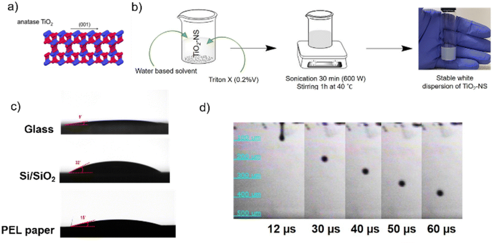 | ||
| Fig. 1 (a) Structure of TiO2-NS; (b) schematic of the TiO2-NS ink formulation process; (c) droplet jetting sequence observed by the Dimatix printer camera; and (d) contact angles of the TiO2-NS ink on glass, Si/SiO2 and PEL-P60 paper substrates, respectively. | ||
In our work, 2D anatase TiO2-NS have been produced using a topochemical approach, which does not require any toxic capping agent and provides a narrow distribution in the size and thickness.35 Our approach, based on NS, has the following advantages as compared to NPs: (i) synthesis of TiO2 nanoparticles typically requires a temperature above 400 °C or thermal annealing; (ii) the NPs are often given by a mixture of different polymorphs or they are doped or mixed with other materials, such as polymers, which are typically used to achieve colloidal stability.36,37 (iii) In the framework of a fully printed device made of 2D materials, it is expected that better contacts between the interfaces will be achieved if 2D materials are used for all device components as this will maximize the van der Waals interactions between NS and minimizes the void fraction in the film. We formulate anatase TiO2-NS into inkjet printable formulations and exploit them in fully printed devices, such as transistors and diodes, with sub-micrometer dielectric thickness, showing the potential of anatase TiO2-NS inks in printed electronics.
Experimental
Materials
![[thin space (1/6-em)]](https://www.rsc.org/images/entities/char_2009.gif) :50 v/v, and twice with pure water. Afterward, the TiS2-NS were re-dispersed in pure water, and hydrogen peroxide (H2O2, 30%, Sigma-Aldrich) was added. The mixture was sealed into a Teflon-lined stainless steel autoclave and heated at 180 °C for 3 h to ensure the chemical conversion of TiS2-NS to TiO2-NS under supercritical conditions. To formulate the ink, the TiO2-NS collected by centrifugation were dispersed in a water-based printable solvent, as described in ref. 13. 0.2%V of Triton 100-X (Sigma-Aldrich) was subsequently added, and the ink was continuously stirred for 1 h at 40 °C. Finally, the ink was sonicated at 600 W using a Hilsonic bath sonicator for 30 minutes. A TiO2-NS concentration of ∼1 mg mL−1 was used for printing all devices.
:50 v/v, and twice with pure water. Afterward, the TiS2-NS were re-dispersed in pure water, and hydrogen peroxide (H2O2, 30%, Sigma-Aldrich) was added. The mixture was sealed into a Teflon-lined stainless steel autoclave and heated at 180 °C for 3 h to ensure the chemical conversion of TiS2-NS to TiO2-NS under supercritical conditions. To formulate the ink, the TiO2-NS collected by centrifugation were dispersed in a water-based printable solvent, as described in ref. 13. 0.2%V of Triton 100-X (Sigma-Aldrich) was subsequently added, and the ink was continuously stirred for 1 h at 40 °C. Finally, the ink was sonicated at 600 W using a Hilsonic bath sonicator for 30 minutes. A TiO2-NS concentration of ∼1 mg mL−1 was used for printing all devices.
Ink characterization
The surface tension was measured using a Theta Lite 101 optical tensiometer by the pendant drop method (Biolin Scientific). The shape of the drop suspended from a needle results from the relationship between the surface tension and gravity. The surface tension is then calculated from the shadow image of a pendant drop using OneAttension analysis software. Dynamic viscosity was determined with a Brookfield DVII + Pro viscometer at varying shear rates and at room temperature. The absorption measurements were performed using a PerkinElmer I-900 UV-vis-NIR spectrometer.Device fabrication
A Dimatix inkjet printer (DMP-2800, FujiFilm) equipped with a 10 pL cartridge was used. Inks were printed onto various types of substrates: clean microscope glass slides (Fisher Scientific Clear Glass Slides, 1.0–1.2 mm thickness), Si/SiO2 substrate (Inseto Ltd), and technical paper (PEL P60, from Printed Electronics Ltd). Capacitors were fabricated on glass by printing the graphene ink for the electrodes and the TiO2-NS ink as dielectric, in a vertical configuration. For both the top and bottom graphene electrodes, 60 printing passes were used with a drop spacing of 40 μm, while the TiO2 dielectric film was deposited using 60, 80 and 100 print passes. Each printed film was annealed after printing at 150 °C under vacuum. For the diode fabrication, the Ag contacts and the CNT networks were printed with a single pass, while the TiO2 film was printed with 20 and 40 print passes. Two thermal treatments at 200 °C were carried out after TiO2 NS printing and fabrication of the whole device. For the transistors, the Ag contacts were printed with a single pass, while the TiO2 film was printed with 80 print passes.Film characterization
The thickness and the roughness of the printed TiO2 films were measured using a Bruker Dektak XT surface profiler (a stylus radius of 12.5 μm, a stylus force of 2 mg, a scan speed of 100 μm s−1, and a scan resolution of 0.33 μm). The Raman spectroscopy measurements were performed using a Renishaw inVia Raman spectrometer equipped with a laser with a 514.5 nm excitation wavelength and 0.5 mW power. A 100× objective and a grating of 2400 g mm−1 were used. Surface morphology was visualized using scanning electron microscopy (Zeiss Gemini Ultra55).Electrical measurements
Impedance measurements were performed in vacuum exploiting a Keysight E4980A Precision LCR meter with short-circuit and open-circuit corrections (bias voltage, Vb = 0 V and measurement voltage, Vm = 1 V) and collected from 1 kHz to 1 MHz. For each capacitor, both the capacitance value (Cp) and its parallel resistance (Rp), representing the leakage through the dielectric, were measured. The capacitor electrode was connected to the measurement system through the tip of the probe station, touching a previously defined silver pad. Cable parasitic capacitances were de-embedded through a four-probe measurement configuration. Measurements for diodes and transistors were carried out in air using a Keithley 4200A-SCS Parameter Analyzer.Results
Ink preparation and printability
The TiO2 nanosheets have a lateral size of 40 ± 30 nm, a thickness of 4 ± 3 nm, and a bandgap of ∼3.5 eV, as characterized in ref. 35. The distributions, in particular for the lateral size, are narrower than those of h-BN NS produced by LPE (e.g. 152 ± 61 nm and 6 ± 4 nm for the lateral size and thickness, respectively).16 The small size of the NS makes them suitable to be formulated into an ink-jet printable ink.To produce an ink with appropriate rheological properties for (piezoelectric) inkjet printing, the TiO2-NS were dispersed in a printable water-based solvent developed previously in our group. Water alone cannot be used as a printable solvent as it does not provide stable droplet formation.13 Furthermore, 0.2%v of Triton X-100 was added to act as a dispersion agent to improve the colloidal suspension stability of the nanosheets – TiO2 is known for being difficult to disperse in water.40,41 Furthermore, this non-ionic surfactant also reduces the surface tension of the ink from 51 to 32 mN m−1, allowing for adequate ink wettability and droplet spreading. A white and stable (for at least 1 month, based on visual inspection) dispersion of TiO2-NS has been successfully obtained (Fig. 1b).
In order to optimize the printing, it is important to evaluate the dimensionless Z number (i.e. the inverse of the Ohnesorge number), which determines the ratio between surface tension forces (Reynolds number – Re) and viscous forces (Weber number – We) according to the following equation:42
As depicted in Fig. S1,† the dynamic viscosity of the TiO2-NS ink decreases as the shear rate increases, indicating non-Newtonian behavior caused by the addition of the binder component to the ink solvent formulation.13 The ink viscosity value collected at the highest shear rate (η = 2.53 mPa s) and the surface tension value measured using the pendant drop method (γ = 32 mN m−1), resulting in Z ∼ 10, which is below the maximum recommended value and predicts successful printability. Fig. 1c shows the wetting behavior of the TiO2-NS ink, where the average contact angles were found to be ∼9°, ∼32° and ∼15° on glass, Si/SiO2 and PEL paper substrates, respectively. Low contact angle values ensure the good spread of the ink once deposited on the substrates under optimized drop spacing. The latter is a critical parameter for controlling the printed film thickness and continuity. Indeed, a small drop spacing results in a thick film with bulges around the edges, lowering the printed pattern's resolution, whereas too a large drop spacing produces a train of distinct droplets with no overlap. Fig. 1d shows the stroboscopic images of ink droplet formation versus time: a steady droplet with a near-spherical shape ejected using a 17 ± 2 V firing voltage at 5 kHz is observed. The short filament (tail) formed behind the rounded main drop quickly pulls on the head, and the entire mass shrinks into a single droplet that detaches smoothly from the nozzle without any visible satellite droplets.
As illustrated in the optical micrographs of Fig. S2,† uniform and continuous TiO2-NS printed lines were successfully printed using an optimal drop spacing of 30 μm on paper and glass, and 35 μm on Si/SiO2. The substrate holder was maintained at 45 °C during inkjet printing in order to promote solvent evaporation and limit the loss of resolution of the printed pattern when printing multiple layers.2,44 The inkjet parameters set to print uniform and continuous TiO2-NS lines on different substrates are summarized in Table S1.†
The ink was formulated with a final concentration of ∼1 mg mL−1 and printed using different passes. The height profiles of TiO2-NS lines printed on glass with various print passes (Fig. 2a and Fig. S2†) reveal reasonably uniform thicknesses with no noticeable high spikes at the profile edge, indicating a negligible coffee-stain effect. The mean height of the printed lines is plotted as a function of the number of passes, as shown in Fig. 2b, showing that the average thickness increases linearly with the number of printing passes for the same ink concentration.
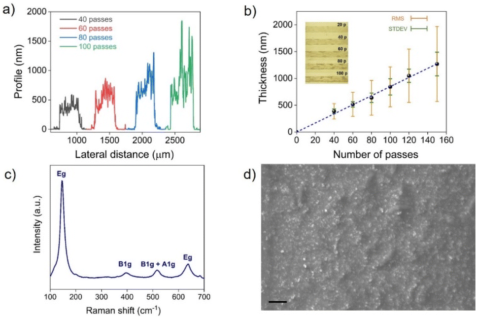 | ||
| Fig. 2 (a) Surface profiles of inkjet-printed TiO2-NS lines on the glass substrate measured by profilometry. (b) Average thickness of the printed TiO2-NS lines on glass substrate plotted as a function of the number of passes. RMS = root mean square, STDEV = standard deviation. (c) Raman spectrum of the TiO2-NS film printed on the glass substrate. (d) Top-view SEM image of a printed film dried at 45 °C (platen temperature), scale bar = 2 μm. | ||
For 40 printed passes of TiO2, the average film thickness is ∼380 ± 40 nm, with a root mean square roughness of 143 nm. For 150 printed passes, these values increase to ∼1.3 ± 0.2 μm and ∼700 nm, respectively. The Raman spectrum measured on the printed TiO2-NS film (Fig. 2c) reveals the characteristic vibrational mode of the anatase TiO2 phase, namely the Eg peak (at 144 cm−1), B1g peak (at 394 cm−1), and Eg peak (at 638 cm−1), and the A1g + B1g modes centered around 515 cm−1, respectively.45,46 The top-view SEM image of the printed TiO2-NS film dried at 45 °C shows continuous features without cracks or pinholes, illustrating the high quality of the printed films (Fig. 2d).
Fully printed capacitors
Graphene/TiO2-NS/graphene capacitors were fabricated by printing the TiO2-NS ink as a dielectric between two graphene electrodes, printed onto a glass substrate in a vertical stacking configuration, as shown in Fig. 3a. A rectangle-shaped TiO2-NS film with a width w ≈ 500 μm and a length l ≈ 800 μm was printed over the graphene bottom electrode (l = 3 mm; w ≈ 150 μm). Then, the graphene top electrode (l = 3 mm; w ≈ 150–350 μm) was printed transversally to the bottom electrode, crossing the center of the TiO2-NS layer (Fig. 3b). To avoid remixing of the TiO2-NS at the interface, an intermediate annealing step at 150 °C was introduced after printing each material. Fig. 3b depicts the capacitor layout under an optical microscope. A picture of 12 devices printed on glass is shown in Fig. 3c.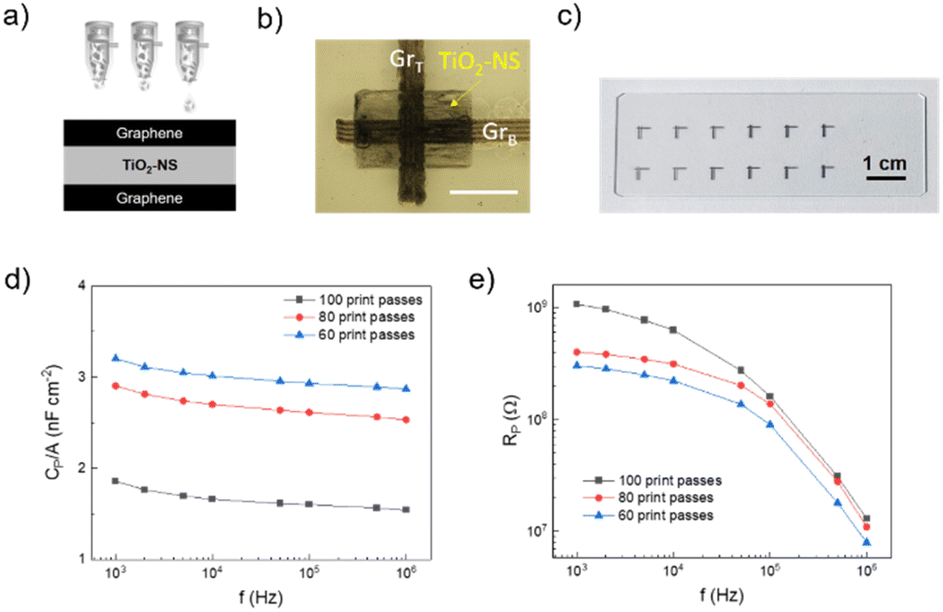 | ||
| Fig. 3 (a) Schematic diagram of the cross-section of the graphene/TiO2-NS/graphene capacitors. (b) Photograph of the inkjet-printed capacitor devices on glass. Scale bar ∼500 μm. (c) Optical micrograph of fully inkjet-printed capacitors on glass. (d) Measured capacitance versus frequency for inkjet-printed capacitors made with different numbers of TiO2-NS print passes. (e) Resistance values versus frequency of inkjet-printed capacitors made with different numbers of print passes. | ||
Fig. 3d and e show the variations of the areal capacitance (Cp/A, where A is the electrode overlapped area) and the parallel resistance (Rp) values, measured in vacuum, as a function of frequency, ranging from 1 kHz to 1 MHz, for devices made with different numbers of TiO2-NS printing passes. It can be seen that Cp exhibits only a slight frequency-dependent variation, while Rp decreases as the frequency increases. As expected for parallel plate capacitors, devices made with fewer TiO2-NS print passes, associated with a thinner dielectric film thickness, exhibit higher areal capacitance and lower resistance when compared to devices made with higher number of print passes. The areal capacitance was approximately 3 nF cm−2 for 60 print passes, corresponding to a dielectric thickness of ∼520 ± 50 nm, confirming the successful formation of a sub-micrometer pinhole-free dielectric layer. The relative dielectric constant (εr) was determined using the equation:47C = εrε0A/t, where ε0 is the dielectric constant in vacuum and t is the dielectric thickness. Fig. S3† displays the linear fitting of the capacitance plotted against the ratio of area to thickness, giving εr ≈ 2.2, which is comparable to that of the printed h-BN,16 although lower than those of other printable materials such as layered bismuth oxychloride48 and composite dielectrics.49
The breakdown voltage of the printed TiO2-NS dielectric film was determined by gradually increasing the applied voltage until device breakdown occurred. The average (over 3 devices) breakdown voltage was found to be ∼880 ± 170 V, which corresponds to an average dielectric strength of 8.8 ± 1.7 MV cm−1, comparable to those of typical dielectric oxide materials, i.e. ZrO2 (∼7 MV cm−1),50 SiO2 (9 MV cm−1)51 and Al2O3 (7 MV cm−1),52 deposited by thermal evaporation or atomic layer deposition. Moreover, we can observe that the dielectric strength of the printed TiO2-NS layer is higher than that of other printable solution-processed materials, such as layered bismuth oxychloride (0.67 MV cm−1l),48 inkjet printed h-BN (1.93 MV cm−1)16 and triacetate cellulose (1.54 MV cm−1).53 Table S2 in the ESI† provides a short overview comparing the dielectric properties of TiO2 NS with those of other printable solution-processed materials.
Printed diodes and transistors
As a further demonstration of the potential of the TiO2-NS ink as a dielectric layer for printed devices, we fabricated printed metal–insulator–semiconductor (MIS) diodes.54,55 A sketch of the longitudinal cross-section of the proposed structure is depicted in the inset of Fig. 4a, which consists of a semiconductive and the TiO2-NS insulator layer deposited between two metallic contacts. First, the Ag ink is inkjet-printed to fabricate the contact, followed by the printing of the TiO2 films. The semiconductor layer consists of an inkjet-printed network of CNT, whose overlap with the TiO2-NS film defines the active area of the device. Finally, a second Ag electrode is printed, contacting the CNT network.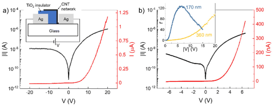 | ||
| Fig. 4 (a) I–V characteristics of a printed MIS diode on both a semilogarithmic (left axis, black curve) and linear (right axis, red curve) scale. The average TiO2-NS thickness is 360 nm. The inset shows a sketch of the longitudinal section of the structure. (b) I–V characteristics of a nominally identical printed MIS diode but with an average TiO2-NS thickness of 170 nm. The inset shows the rectification ratio as a function of the modulus of the applied voltage for the two diodes with different TiO2-NS thicknesses. The active area of the diodes is approximately 200 μm × 100 μm. | ||
The insulator thickness plays a key role in the current–voltage (I–V) characteristics of the device. Indeed, a large thickness would not allow any current flow, resulting in a non-rectifying device with very low current densities. On the other hand, a too thin layer would lead to a short-circuit between CNT and the bottom Ag contact, because of the presence of many pinholes in the insulator.
Fig. 4a shows the I–V characteristics, on both semilogarithmic and linear scales, of a diode having an average TiO2-NS thickness of ∼360 nm in the ±20 V voltage range. The measurement was carried out biasing the device according to the polarity shown in the inset of Fig. 4a, that is, with the anode formed by the Ag electrode in contact with the CNT. The device is rectifying and has a rectification ratio (r) of ∼100 at |20| V, where r is defined as the ratio between the forward current (for positive V) and the reverse current (for negative V).
It is possible to further decrease the insulator thickness in order to improve both the current density and r. Fig. 4b shows the I–V characteristics of a diode with the same geometry, but with an average TiO2-NS thickness of ∼170 nm. With respect to the previous case, the diode has a higher forward current density and a good rectification (r ≈ 130) even with low supply voltages (of the order of 5 V), making it suitable for low-voltage applications.
The inset of Fig. 4b shows the rectification ratio of the MIS diode as a function of the applied voltage. The diode with a thicker insulator has a monotonic r with respect to V, and thus requires relatively high bias voltages to achieve good rectification, while the diode with a thinner TiO2-NS film exhibits a maximum r of 130 at about 6.5 V, and then decreases due to the increase in the reverse current.
We finally demonstrate that the printed TiO2-NS film can be employed as a gate dielectric for field-effect transistors printed on paper. This substrate has been chosen because it is inexpensive, recyclable and flexible, and hence extremely promising for future flexible electronics applications. CVD MoS2, used as a channel, is transferred onto paper, while the drain and source contacts are inkjet printed using the Ag ink. Then, the TiO2-NS film is inkjet printed on top of the contacts and the semiconductor. Finally, the Ag gate contact is printed over the dielectric. A sketch of the longitudinal section and optical micrographs of the device, before and after TiO2-NS printing, is shown in the insets of Fig. 5a and b, respectively.
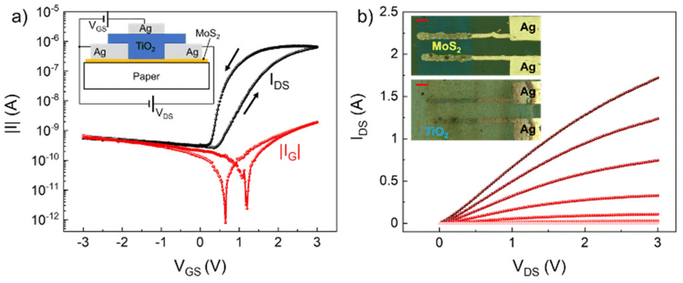 | ||
| Fig. 5 (a) Channel current (black curve) and gate current (red curve) as a function of VGS with VDS = 2 V. In the inset, a sketch of the longitudinal section of the structure, showing its layer sequence and biasing voltages. (b) Output characteristics measured for VGS ranging from −1 to 3 V, with a step of 0.5 V. The inset shows optical micrographs of a device before and after TiO2 printing. The scale bars are 100 μm. | ||
Fig. 5a and b show the transfer characteristics (for the drain-to-source voltage, VDS = 2 V), and the output characteristics (measured for the gate-to-drain voltage VGS ranging from −1 V to 3 V) of a transistor having a channel length and width of 120 and 450 μm, respectively. In Fig. 5a, along with the channel current IDS, the gate leakage current IG is also shown. As can be observed, the channel current of the transistor is effectively modulated (more than three orders of magnitude) with low applied voltages (<3 V), while IG is <2 nA over the entire voltage range, further demonstrating the good insulating properties of the printed TiO2 films. The hysteresis visible from the transfer characteristics may be due to either the charge carriers interacting with shallow traps at the semiconductor/dielectric interface, or the presence of slow-moving ions in the dielectric when sweeping VGS.56
Conclusions
In this work, we formulated a stable, water-based ink of anatase TiO2-NS, suitable for inkjet printing. The TiO2-NS printed films of ∼520 nm have a relative dielectric constant of ∼2.2 and an average breakdown voltage of ∼880 ± 170 V. To note that the dielectric constant could be further increased by post-processing, for example, by inducing phase transformation or by defect or doping engineering strategies. We finally show the suitability of the ink in printed electronics by demonstrating printed diodes and transistors, where the inkjet-printed TiO2-NS is used as a gate dielectric. We observed effective modulation of the channel with low voltages despite the relatively thick TiO2-NS films – this could be explained by the formation of an electric double layer,57,58 but further works are needed to confirm this explanation.Author contributions
Conceptualization and methodology: materials (CC) and devices (CC and GF). Data curation and investigation: OK, LP, CD, MZ, DKP, ED, GB, FP, and LC. Supervision: CC, GF, JU, and TM. Writing: original draft (OK and LP); review (GF and CC).Conflicts of interest
There are no conflicts to declare.Acknowledgements
This work is supported by the H2020 WASP project (grant agreement no. 825213), the Graphene Flagship Core 3 (Contract no. 881603) and the ERC Project PEP2P (contract no. 770047). MZ acknowledges the financial support by HP. DD and JJU acknowledge the Office of Science, Office of Basic Energy Sciences, of the U.S. Department of Energy under Contract no. DE-AC02-05CH11231.References
- S. K. Garlapati, M. Divya, B. Breitung, R. Kruk, H. Hahn and S. Dasgupta, Adv. Mater., 2018, 30, 1–55 CrossRef PubMed.
- O. Kassem, M. Saadaoui, M. Rieu and J. P. Viricelle, J. Mater. Chem. C, 2019, 7, 12343–12353 RSC.
- Y. Khan, A. Thielens, S. Muin, J. Ting, C. Baumbauer and A. C. Arias, Adv. Mater., 2020, 32, 1–29 CrossRef PubMed.
- C.-Y. Yang, M.-A. Stoeckel, T.-P. Ruoko, H.-Y. Wu, X. Liu, S. A. Jenekhe, M. Berggren and S. Fabiano, Nat. Commun., 2021, 12, 2354 CrossRef CAS PubMed.
- E. B. Secor and M. C. Hersam, J. Phys. Chem. Lett., 2015, 6, 620–626 CrossRef CAS PubMed.
- G. Hu, J. Kang, L. W. T. Ng, X. Zhu, R. C. T. Howe, C. G. Jones, M. C. Hersam and T. Hasan, Chem. Soc. Rev., 2018, 47, 3265–3300 RSC.
- Z. Lin, Y. Liu, U. Halim, M. Ding, Y. Liu, Y. Wang, C. Jia, P. Chen, X. Duan, C. Wang, F. Song, M. Li, C. Wan, Y. Huang and X. Duan, Nature, 2018, 562, 254–258 CrossRef CAS PubMed.
- X. Cai, Y. Luo, B. Liu and H.-M. Cheng, Chem. Soc. Rev., 2018, 47, 6224–6266 RSC.
- A. G. Kelly, D. O'Suilleabhain, C. Gabbett and J. N. Coleman, Nat. Rev. Mater., 2022, 7, 217–234 CrossRef CAS.
- S. Pinilla, J. Coelho, K. Li, J. Liu and V. Nicolosi, Nat. Rev. Mater., 2022, 7, 717–735 CrossRef.
- Y. Hernandez, V. Nicolosi, M. Lotya, F. M. Blighe, Z. Sun, S. De, I. T. McGovern, B. Holland, M. Byrne, Y. K. Gun'Ko, J. J. Boland, P. Niraj, G. Duesberg, S. Krishnamurthy, R. Goodhue, J. Hutchison, V. Scardaci, A. C. Ferrari and J. N. Coleman, Nat. Nanotechnol., 2008, 3, 563–568 CrossRef CAS PubMed.
- V. Nicolosi, M. Chhowalla, M. G. Kanatzidis, M. S. Strano and J. N. Coleman, Science, 2013, 340, 1226419 CrossRef.
- D. McManus, S. Vranic, F. Withers, V. Sanchez-Romaguera, M. Macucci, H. Yang, R. Sorrentino, K. Parvez, S. K. Son, G. Iannaccone, K. Kostarelos, G. Fiori and C. Casiraghi, Nat. Nanotechnol., 2017, 12, 343–350 CrossRef CAS PubMed.
- A. G. Kelly, T. Hallam, C. Backes, A. Harvey, A. S. Esmaeily, I. Godwin, J. Coelho, V. Nicolosi, J. Lauth, A. Kulkarni, S. Kinge, L. D. A. Siebbeles, G. S. Duesberg and J. N. Coleman, Science, 2017, 356, 69–73 CrossRef CAS PubMed.
- T. Carey, S. Cacovich, G. Divitini, J. Ren, A. Mansouri, J. M. Kim, C. Wang, C. Ducati, R. Sordan and F. Torrisi, Nat. Commun., 2017, 8, 1202 CrossRef PubMed.
- R. Worsley, L. Pimpolari, D. McManus, N. Ge, R. Ionescu, J. A. Wittkopf, A. Alieva, G. Basso, M. MacUcci, G. Iannaccone, K. S. Novoselov, H. Holder, G. Fiori and C. Casiraghi, ACS Nano, 2019, 13, 54–60 CrossRef CAS PubMed.
- J. Kim, D. Rhee, O. Song, M. Kim, Y. H. Kwon, D. Un Lim, I. Soo Kim, V. Mazánek, L. Valdman, Z. Sofer, J. Ho Cho and J. Kang, Adv. Mater., 2022, 34, 2106110 CrossRef CAS PubMed.
- K. Zhang, Y. Feng, F. Wang, Z. Yang and J. Wang, J. Mater. Chem. C, 2017, 11992–12022 RSC.
- R. Ma and T. Sasaki, Adv. Mater., 2010, 22, 5082–5104 CrossRef CAS PubMed.
- M. Osada, G. Takanashi, B.-W. Li, K. Akatsuka, Y. Ebina, K. Ono, H. Funakubo, K. Takada and T. Sasaki, Adv. Funct. Mater., 2011, 21, 3482–3487 CrossRef CAS.
- L. Wang and T. Sasaki, Chem. Rev., 2014, 114, 9455–9486 CrossRef CAS PubMed.
- S. Reghunath, D. Pinheiro and S. D. Kr, Appl. Surf. Sci. Adv., 2021, 3, 100063 CrossRef.
- R. Li, X. Ma, J. Li, J. Cao, H. Gao, T. Li, X. Zhang, L. Wang, Q. Zhang, G. Wang, C. Hou, Y. Li, T. Palacios, Y. Lin, H. Wang and X. Ling, Nat. Commun., 2021, 12, 1587 CrossRef CAS PubMed.
- B. Lyu, Y. Choi, H. Jing, C. Qian, H. Kang, S. Lee and J. Ho Cho, Adv. Mater., 2020, 32, 1907633 CrossRef CAS PubMed.
- L. Sheng, T. Liao, L. Kou and Z. Sun, Mater. Today Energy, 2017, 3, 32–39 CrossRef.
- M. Gong, Y. Li, Y. Guo, X. Lv and X. Dou, Sens. Actuators, B, 2018, 262, 350–358 CrossRef CAS.
- J. Yu, Y. Zhang, J. Chen, L. Cui and W. Jing, J. Membr. Sci., 2020, 600, 117870 CrossRef CAS.
- M. Černá, M. Veselý, P. Dzik, C. Guillard, E. Puzenat and M. Lepičová, Appl. Catal., B, 2013, 138–139, 84–94 CrossRef.
- A. J. Huckaba, Y. Lee, R. Xia, S. Paek, V. C. Bassetto, E. Oveisi, A. Lesch, S. Kinge, P. J. Dyson, H. Girault and M. K. Nazeeruddin, Energy Technol., 2019, 7, 317–324 CrossRef CAS.
- H. Maleki and V. Bertola, ACS Appl. Nano Mater., 2019, 2, 7237–7244 CrossRef CAS.
- M. Buffiere, K. Ali, E. Fares, A. Samara, A. R. Shetty, O. Al Hassan and A. Belaidi, Energy Technol., 2020, 8, 2000330 CrossRef CAS.
- H. G. Yang, C. H. Sun, S. Z. Qiao, J. Zou, G. Liu, S. C. Smith, H. M. Cheng and G. Q. Lu, Nature, 2008, 453, 638–641 CrossRef CAS PubMed.
- J. Yu, Q. Xiang, J. Ran and S. Mann, CrystEngComm, 2010, 12, 872–879 RSC.
- B. Chen, J. Sha, W. Li, F. He, E. Liu, C. Shi, C. He, J. Li and N. Zhao, ACS Appl. Mater. Interfaces, 2016, 8, 2495–2504 CrossRef CAS PubMed.
- M. Zarattini, C. Dun, L. H. Isherwood, A. Felten, J. Filippi, M. P. Gordon, L. Zhang, O. Kassem, X. Song, W. Zhang, R. Ionescu, J. A. Wittkopf, A. Baidak, H. Holder, C. Santoro, A. Lavacchi, J. J. Urban and C. Casiraghi, J. Mater. Chem. A, 2022, 10, 13884–13894 RSC.
- B. Balasubramanian, K. L. Kraemer, N. A. Reding, R. Skomski, S. Ducharme and D. J. Sellmyer, ACS Nano, 2010, 4, 1893–1900 CrossRef CAS PubMed.
- Y. Yang, Z. Xu, T. Qiu, H. Ning, J. Zhong, M. Li, D. Luo, X. Liu, R. Yao and J. Peng, Org. Electron., 2022, 101, 106413 CrossRef CAS.
- H. Yang, Y. Hernandez, A. Schlierf, A. Felten, A. Eckmann, S. Johal, P. Louette, J. J. Pireaux, X. Feng, K. Mullen, V. Palermo and C. Casiraghi, Carbon, 2013, 53, 357–365 CrossRef CAS.
- S. Conti, L. Pimpolari, G. Calabrese, R. Worsley, S. Majee, D. K. Polyushkin, M. Paur, S. Pace, D. H. Keum, F. Fabbri, G. Iannaccone, M. Macucci, C. Coletti, T. Mueller, C. Casiraghi and G. Fiori, Nat. Commun., 2020, 11, 3566 CrossRef CAS PubMed.
- W.-B. Tsai, J.-Y. Kao, T.-M. Wu and W.-T. Cheng, J. Nanopart., 2016, 2016, 1–9 CrossRef.
- J. Y. Kao and W. T. Cheng, ACS Omega, 2020, 5, 1832–1839 CrossRef CAS PubMed.
- Y. Liu and B. Derby, Phys. Fluids, 2019, 31, 032004 CrossRef.
- N. Reis and B. Derby, Mater. Res. Soc. Symp. Proc., 2000, 625, 3–8 CrossRef.
- C. Gaspar, T. Sikanen, S. Franssila and V. Jokinen, Biomicrofluidics, 2016, 10, 064120 CrossRef PubMed.
- H. Berger, H. Tang and F. Lévy, J. Cryst. Growth, 1993, 130, 108–112 CrossRef CAS.
- W. F. Zhang, Y. L. He, M. S. Zhang, Z. Yin and Q. Chen, J. Phys. D: Appl. Phys., 2000, 33, 912–916 CrossRef CAS.
- A. G. Kelly, D. Finn, A. Harvey, T. Hallam and J. N. Coleman, Appl. Phys. Lett., 2016, 109, 023107 CrossRef.
- Y. Nalawade, J. Pepper, A. Harvey, A. Griffin, D. Caffrey, A. G. Kelly and J. N. Coleman, ACS Appl. Electron. Mater., 2020, 2, 3233–3241 CrossRef CAS.
- X. Cao, H. Chen, X. Gu, B. Liu, W. Wang, Y. Cao, F. Wu and C. Zhou, ACS Nano, 2014, 8, 12769–12776 CrossRef CAS PubMed.
- K. Kukli, J. Niinistö, A. Tamm, M. Ritala and M. Leskelä, J. Vac. Sci. Technol., B: Microelectron. Nanometer Struct.–Process., Meas., Phenom., 2009, 27, 226 CrossRef CAS.
- N. R. Glavin, C. Muratore, M. L. Jespersen, J. Hu, P. T. Hagerty, T. S. Fisher and A. A. Voevodin, Adv. Funct. Mater., 2016, 26, 2640–2647 CrossRef CAS.
- J. Yota, H. Shen and R. Ramanathan, J. Vac. Sci. Technol., A, 2013, 31, 01A134 CrossRef.
- J. W. Bae, H.-S. Jang, W.-H. Park and S.-Y. Kim, Org. Electron., 2017, 41, 186–189 CrossRef CAS.
- K. Y. Mitra, C. Sternkiker, C. Martínez-Domingo, E. Sowade, E. Ramon, J. Carrabina, H. L. Gomes and R. R. Baumann, Flexible Printed Electron., 2017, 2, 015003 CrossRef.
- C. Martínez-Domingo, S. Conti, L. Terés, H. L. Gomes and E. Ramon, Org. Electron., 2018, 62, 335–341 CrossRef.
- M. Egginger, S. Bauer, R. Schwödiauer, H. Neugebauer and N. S. Sariciftci, Monatsh. Chem., 2009, 140, 735–750 CrossRef CAS.
- W. Huang, J. Chen, G. Wang, Y. Yao, X. Zhuang, R. M. Pankow, Y. Cheng, T. J. Marks and A. Facchetti, J. Mater. Chem. C, 2021, 9, 9348 RSC.
- B. N. Smith, H. Meikle, J. L. Doherty, S. Lu, G. Tutoni, M. L. Becker, M. J. Therien and A. D. Franklin, Nanoscale, 2022, 14, 16845 RSC.
Footnote |
| † Electronic supplementary information (ESI) available: Additional data on the ink and capacitor characterization. See DOI: https://doi.org/10.1039/d2nr05786g |
| This journal is © The Royal Society of Chemistry 2023 |